Note : Les descriptions sont présentées dans la langue officielle dans laquelle elles ont été soumises.
CA 02485419 2004-11-08
1
DESCRIPTION
MEMBER FOR SEMICONDUCTOR DEVICE
Technical Field
The present invention relates to a member used for a heat sink, a
radiating substrate, a housing, or the like constituting a semiconductor
device,
and more particularly, a member for a semiconductor device having an
excellent resin bonding property and a semiconductor device using the same.
Background Art
When a material constituting a substrate, which is one of the members
for a semiconductor device, is combined with a member for another device, it
is
necessary that distortion due to thermal stress does not occur in the
interface
between the combined members. For this reason, the thermal expansion
coefficient of the substrate material must not be largely different from those
of
other members for the semiconductor device, such as semiconductor elements
or packages. In particular, as the semiconductor device has recently been
made small and lightweight, the radiating substrate is required to be made of
a material of a high thermal conductivity, the thermal expansion coefficient
not being largely different from those of the semiconductor elements or
package, or the like, and light weight.
As a suitable substrate material satisfying these requirements, there is
known an alloy or composite mainly composed of Cu and W and/or Mo, that is,
CA 02485419 2004-11-08
2
a Cu-W or Cu-Mo alloy or composite. In addition, there are known an alloy or
composite mainly composed of Al-SiC and having SiC particles dispersed in Al
or an Al alloy, and an alloy or composite mainly composed of Si-SiC and having
SiC particles dispersed in Si or an SiC alloy.
In addition, the member for a semiconductor device, including the
radiating substrate, is required to have high corrosion resistance. However,
an alloy or composite itself constituting the member does not have corrosion
resistance. Therefore, conventionally, a plating Iayer of Ni or Au or others
was provided on the surface of the alloy or composite. The plating layer has
also been needed to maintain wettability or banding strength during a
conventional process of soldering the substrate material with a package
material, or the Like.
However, recently, instead of the soldering method, a resin bonding
method has been widely used as a method of bonding the radiating substrate
to the package, or the like because the resin bonding method is inexpensive
and can be performed at a low temperature. In a conventional package, etc.
using a resin, before the plating, the radiating substrate and other members
for a semiconductor device, such as a lead frame, are bonded by using a
method, such as a transfer molding method, and then, subjected to the plating.
However, in a recent method, the radiating substrate, for example, is
subjected
to the plating in advance, and then, bonded to the package substrate with a
liquid resin of epoxy or palyimide or a sheet-shaped resin or others.
The problem with the resin bonding method is that, since Ni or Au
CA 02485419 2004-11-08
3
conventionally used as the plating layer has an inferior resin bonding
property,
a required bonding strength cannot be obtained. In particular, after various
reliability tests, such as a thermal cycling test for performing alternate
exposure to temperatures of I50°C and -65°C, a PCT (pressure
cooker test)
performed under a condition of I2I°C, 100% RH (relative humidity), and
2 atm,
and an HAST (highly accelerated stress test) performed under a condition of
131°C, 85% RH, and 2 atm, the resin bonding strength is severely
deteriorated.
On the other had, metallic materials having an excellent resin bonding
property include A1 and Cu on the surface of which a naturally oxidized film
can be easily formed. However, in Al and Cu, the bonding strength between
the naturally oxidized film and the resin is not sufficient, particularly
after the
aforementioned various reliability tests. In addition, the alloy or composite
itself mainly composed of Cu and W and/or Mo, such as Cu-W and Cu-Mo,
could not achieve satisfactory resin bonding strength. This is because the
alloy or composite mainly composed of Cu and W andlor Mo has a partial
region on which a naturally oxidized film of Cu is formed, but which has a low
resin bonding strength.
For these reasons, many approaches for improving resin bonding
properties of metallic materials, such as Al or Cu, have been tried, and
various
methods have been proposed. For example, in Japanese Unexamined Patent
Application Publication Nos. S61-295692 and S61-295693, there are disclosed
methods of improving bonding strength between a base member and a resin
insulating layer by depositing or plating an A1 Layer having a thickness of
CA 02485419 2004-11-08
4
approximately 500 ~,m on one surface of the base member of an invar plate or
copper-plated invar plate, and forming wiring circuits with an insulating
layer
of epoxy resin, etc.
In addition, in Japanese Unexamined Patent Application Publication
No. H10-284643, there is disclosed a method of improving bonding strength by
forming an Al coating layer made of crystalline particles having a diameter of
0.1 to 10 ~.m on a Cu-W or Cu-Mo alloy, and forming an oxidation layer having
a thickness of 10 to 800 .~, on a surface of the Al coating layer.
However, as the operating speed of semiconductor elements has
recently been further increased, a larger amount of heat is generated from the
semiconductor elements. Therefore, a further increase of the resin bonding
strength between the substrate and the package is requred further compared
with that in a conventional method. In particular, less deterrioration of the
that the resin bonding strength is required even after a reliability test,
such as
the HAST.
[Patent Document 1]
Japanese Unexamined Patent Application Publication No. 561-295692
[Patent Document 2]
Japanese Unexamined Patent Application Publication No. 561-295693
[Patent Document 3]
Japanese Unexamined Patent Application Publication No. H10-284643
, CA 02485419 2004-11-08
Disclosure of Invention
In consideration of the aforementioned conventional problems, an
object of the present invention is to provide a member for a semiconductor
device made of an alloy or composite of Cu-W, Cu-Mo, Al-SiC, Si-SiC, etc.
5 wherein the member has an excellent resin bonding property capable of
improving resin bonding strength at the time the member fox a semiconductor
device being bonded to another member with resin and maintains a high resin
bonding strength even after various reliability tests, such as a thermal
cycling
test, are performed, and to provide a semiconductor device employing the
member.
In order to achieve the object, according to one aspect, the present
invention provides a member for a semiconductor device having an excellent
resin bonding property, comprising a base member made of an alloy or
composite mainly composed of Cu and W andlor Mo, wherein a coating layer
made of a hard carbon film is provided on at least a surface of the base
member on which another member for the semiconductor device is bonded
with a resin. It is preferable that the alloy or composite mainly composed of
Cu and W and/or Mo contain Cu of 5 to 40% by weight.
In addition, according to another aspect, the present invention provides
a member for a semiconductor device having an excellent resin bonding
property, comprising a base member made of an alloy or composite mainly
composed of Al-SiC, wherein a coating layer made of a hard carbon film is
provided on at least a surface of the base member on which another member
CA 02485419 2004-11-08
6
for the semiconductor device is bonded with a resin. It is preferable that the
alloy or composite mainly composed of Al-SiC contain SiC of 10 to 70% by
weight.
Furthermore, according to still another aspect, the present invention
provides a member for a semiconductor device having an excellent resin
bonding pxoperty, comprising a base member made of an alloy or composite
mainly composed of Si-SiC, wherein a coating layer made of a hard carbon film
is provided on at least a surface of the base member on which another member
for the semiconductor device is bonded with a resin. It is preferable that the
alloy or composite mainly composed of Si-SiC contain Si of 10 to 35% by
weight.
In any one of the members for a semiconductor device according to the
aspects, it is preferable that the coating layer have a thickness of 0.1 to 10
Vim.
It is preferable that the surface of the base member on which the coating
layer
is formed have a surface roughness of 0.1 to 20 ~m in Rmax. Also, it is
1~ preferable that pores in the surface of the base member on which the
coating
layer is formed have a depth of 100 ~m or Iess. Further, it is preferable that
a
plating Iayer of Ni be provided between the coating layer and the surface of
the base member on which the coating layer is formed.
In addition, according to further still another aspect, the present
invention provides a semiconductor device employing the membex for a
semiconductor device according to the aforementioned aspects.
CA 02485419 2004-11-08
7
Brief Description of Drawings
Figure Z is a schematic sectional view showing an example of a member
for a semiconductor device according to the present invention
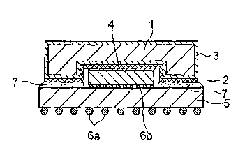
Figure 2 is a schematic sectional view showing a semiconductor device
having the member for a semiconductor device of Fig. 1 bonded to a package
with resin and
Figure 3 is a graph showing the resin bonding strength of a coating
Iayer provided on a surface of a base member.
Best Mode for Carrying Out the Invention
In the present invention, a base member of a member for a
semiconductor device is made of an alloy or composite mainly composed of Cu
and W and/or Mo, an alloy or composite mainly composed of A1-SiC, and an
alloy or composite mainly composed of Si-SiC. These alloys or composites
have a thermal expansion coefficient approximate to those of materials for
semiconductor elements and package, and also an excellent thermal
conductivity. In the present invention, when the member for a semiconductor
device comprising a base member made of these alloys or composites is bonded
to other members, such as a package, with resin, a coating layer made of a
hard carbon film is provided on at least a surface of the base member which is
to be bonded with the resin, so that the resin bonding strength can be
improved.
The hard carbon film is an amorphous carbon film called diamond-like
CA 02485419 2004-11-08
g
carbon, amorphous carbon, i-C, or DLC (diamond-like carbon). The hard
carbon is neither crystalline carbon, such as graphite, nor diamond itself.
The hard carbon film has many properties similar to those of diamond. In
particular, the hard carbon film is a very hard material having a Knoop
strength of 2,000 to 10,000 kg/mm2.
If the hard carbon film is provided as a coating layer to the surface of
the base member of the alloys or composites, it is possible to increase the
resin
bonding strength between the resin and the member for a semiconductor
device comprising a base member made of the alloy or composite mainly
composed of one of W-Cu, Mo-Cu, Al-SiC, and Si-SiC. In addition, since the
resin bonding strength measured after various reliability tests such as a
thermal cycling test is not largely deteriorated, it is possible to maintain
high
resin bonding strength. Such an excellent high resin bonding property is
understood to be derived from an extremely slow reaction velocity of the hard
carbon film and the resin.
The coating layer comprising the hard carbon film has a thickness of
preferably 0.1 to 10 ~,m, more preferably, 0.5 to 1.5 ~,m. If the thickness of
the
hard carbon film is below 0.1 ~,m, a high resin bonding strength can not be
obtained. Particularly, when the thickness is 0.5 ~.m or more, a preferable
resin bonding strength is obtained. In addition, it is undesixrable that the
thickness of the hard carbon film exceed 10 ~.m because the productivity is
lowered. Since the hard carbon film has a high compressive stress, a thicker
film has higher stress, so it can easily be peeled off. Therefore, it is
preferable
CA 02485419 2004-11-08
9
that the thickness of the hard carbon film be below 1.5 ~.m.
The hard carbon film can be formed by using a plasma CVD method, or
an ion beam deposition method, for example. The plasma CVD method is a
method of generating plasma of a carbon-containing source material with high
frequency discharge, direct current discharge, or microwave discharge and
depositing the carbon on the surface of the base member. Since the surface of
the base member is irradiated and activated with plasma, the plasma CVD
method can advantageously form the film at a lower temperature compared
with a thermal CVD method or the like. On the other hand, the ion beam
deposition method is a method of generating plasma from an ion source of
hydrocarbon material such as methane, accelerating the plasma at a discharge
electrode system to form ion beams, and irradiating and depositing the ion
beams on the surface of the base member. In the ion beam deposition method,
as the accelerated ion energy is high, the carbon can further infiltrate the
base
member compared with general deposition methods. Therefore, the ion beam
deposition method advantageously has an excellent bonding property to the
base member.
Comparing the plasma CVD method with the ion beam deposition
method, both of the methods have a common point in generating plasma from
a source material. However, in the plasma CVD method, since the plasma is
not discharged as an ion beam but directly deposited on the base member in
the same space, the film is rapidly farmed and the productivity remarkably
increases. That is, the film formation velocity in the plasma CVD method is
CA 02485419 2004-11-08
three times or more faster than that of the ion beam deposition method, and a
throughput per batch in the plasma CVD method is several to tens times
higher than that of the ion beam deposition method. In addition, since both
of the plasma CVD method and the ion beam method can form the hard carbon
5 film at a low temperature of 200°C or less, the quality of the base
member is
not deteriorated.
The base member having the coating layer comprising the hard carbon
film formed thereon is one of an alloy or composite mainly composed of Cu and
W andlar Mo, an alloy or composite mainly composed of Al~SiC, and an alloy or
10 composite mainly composed of Si-SiC, which conventionally have been used as
a substrate material. For example, the alloy or composite mainly composed of
Cu and W andlor Mo is disclosed in Japanese Unexamined Patent Application
Publication No. 559-21032, No. 559-46050, etc. In addition, the alloy or
composite mainly composed of Al-SiC is disclosed in Japanese Unexamined
Patent Application Publication No. H10-335538, etc. The alloy or composite
mainly composed of Si-SiC is disclosed in Japanese Unexamined Patent
Application Publication No. 1311-166214, etc.
With respect to a method of manufacturing the hard carbon film, the
alloy or composite mainly composed of Cu and W and/or Mo can be
manufactured by an infiltration method or a sintering method. Tn the
infiltration method, W or/and Mo powder having Cu powder added thereto is
sintered, and Cu is infiltrated into an obtained skeleton. In the sintering
method, a compact of W andlor Ma powder and Cu powder is sintered. Also,
CA 02485419 2004-11-08
11
the alloy or composite mainly composed of AI-SiC can be manufactured by a
method, such as a casting method, an immersion method, or a sintering
method. In the immersion method, A1 is immersed into a preform of SiC. In
the sintering method, a compact of AI powder and SiC powder or a compact of
an Al-SiC alloy or composite is sintered. In addition, the alloy or composite
mainly composed of Si-SiC can be manufactured by a method, such as a
casting method, an immersion method, or a sintering method. In the
immersion method, Si is immersed into a preform of SiC. In the sintering
method, a compact of Si powder and SiC powder or a compact of an Si-SiC
alloy or composite is sintered.
These alloys or composites have excellent thermal conductivity as well
as a thermal expansion coefficient approximate to those of materials for
semiconductor elements and packages. For example, the alloy or composite
mainly composed of Cu and W and/or Mo has a thermal expansion coefficient
of typically 5x10⁻⁶ to 12x10-6/°C in the case of the Cu content being
in a range
of 5 to 40% by weight. The alloy or composite mainly composed of Al-SiC has
a thermal expansion coefficient of $x10'6 to 20x10'61°C in the case of
the SiC
content being in a range of 10 to 70% by weight. The alloy or composite
mainly composed of Si-SiC has a thermal expansion coefficient of
5x10'6/°C or
less over a wide range of content, and particularly, a high thermal
conductivity
of 200 W/m~K or more in the case of the Si content being in a range of 10 to
35% by weight.
On the other hand, a generally used semiconductor element made of Si,
CA 02485419 2004-11-08
12
Ge, GaAs, etc. has a thermal expansion coefficient of approximately 3x10⁻⁶ to
4x10⁶/°C. A package member bonded to a substrate has a thermal
expansion
coefficient of approximately 4x10'6 to lOxI0~6/°C in the case of a
generally used
ceramic package and approximately 7x10⁻⁶ to 13x106/°C in the case of a
plastic
package. Therefore, it is preferable that the alloy or composite mainly
composed of Cu and W and/or Mo contain Cu of 5 to 40% by weight. It is
preferable that the alloy or composite mainly composed of Al-SiC contain SiC
of 10 to 70% by weight. It is preferable that the alloy or composite mainly
composed of Si-SiC contain SiC of I0 to 35% by weight.
Preferably, the surface of the base member on which the coating layer
of the hard carbon film is formed, is controlled to have surface roughness of
0.1
to 20 ~m in Rmax (maximum height) in accordance with the ~IIS specification.
If the surface roughness is less than 0.1 ~.m in Rmax, a sufficient anchoring
effect cannot be obtained even if the coating layer comprising the hard carbon
film is formed on the surface. Also, if the surface roughness is more than 20
~.m in Rmax, adsorption gases, such as oxygen, increase, so a large amount of
gases is released during the coating layer formation. Therefore, it is
difficult
to obtain the degree of vacuum required for the film formation. In addition,
the adhesion between the base member and the coating layer may be lowered.
However, in general, if the surface roughness is more than 8 pm in Rmax,
voids between resin and the surface of the base member are easily formed
during the resin bonding, so variations of the resin bonding strength may
increase. Therefore, it is more preferable that the surface roughness is kept
CA 02485419 2004-11-08
13
at 0.1 to 8 ~m in Rmax.
In addition, in order to satisfy the condition of the surface roughness of
the base member, it is preferable that pores formed in the surface of the base
member have a depth of 100 wm or less. If the pores have a depth of more
than 100 pm, the amount of the adsorption gases on the surface of the base
member increases, and it is difficult to form a uniform thickness of the
coating
layer on the base member. Therefore, pits may be created on the surface of
the coating layer. In addition, since sufficient bonding resin does not
penetrate, it is difficult to maintain a sufficient resin bonding strength.
Furthermore, in order to ensure the bonding strength between the base
member and the hard carbon film by providing corrosion resistance to the base
member, a plating layer of Ni or the Like is formed on the surface of the base
member, which is made of an alloy or composite mainly composed of Cu and W
and/or Mo, an alloy or composite mainly composed of Al-SiC, or an alloy or
composite mainly composed of Si-SiC. More specifically, it is preferable that
electrolytic Ni plating or non~electrolytic Ni-P or Ni-B plating is performed
to
have a film thickness of 1 to 2 pm.
In addition, in order to improve the adhesion of the hard carbon film,
an intermediate layer may be formed between the hard carbon film and the
base member or the plating layer of Ni or the like on the surface of the base
member. For example, the intermediate Iayer is made of amorphous silicon,
polycrystalline silicon, Ge, SiC, or the like. It is preferable that the
thickness
of the intermediate layer be in a range of approximately 5 to 500 nm. If the
CA 02485419 2004-11-08
1
thickness is Iess than 5 nm, it is difficult to coat the surface of the base
member completely, so the intermediate layer cannot have a remarkable effect.
Even though the upper limit of the thickness may be several micrometers, it is
preferable that the thickness be 500 nm or less in consideration of the
productivity.
The intermediate layer may be formed by using any conventional film
formation method including, for example, a PVD method and a CVD method.
In this case, it is effective that the intermediate layer and the hard carbon
film
are continuously formed within the same vacuum chamber or within a multi-
layered vacuum apparatus without releasing the vacuum of the apparatus to
the atmospheric pressure. Since this does not allow the base member to be
exposed to the atmosphere, improved adhesion between the intermediate layer
and the hard carbon film can be expected.
The resin used to bond the member for a semiconductor device
according to the present invention, where the hard carbon film is provided on
the surface of the base member, to another member, such as a package,
includes, for example, epoxy resin to which a silver filler or a ceramic
filler
such as silica is added, epoxy resin to which silicon resin is added to reduce
Young's modulus, epoxy resin without the aforementioned addition, polyimide
resin with the aforementioned addition, polyimide resin without the addition,
phenol resin with the aforementioned addition, phenol resin without the
addition, polyester resin with the aforementioned addition, polyester resin
without the addition, silicon resin with the aforementioned addition, and
CA 02485419 2004-11-08
silicon resin without the addition.
A semiconductor device can be manufactured by using a member
according to the present invention, where a hard carbon film is provided on
the
surface of the base member. For example, as shown in Fig. 1, an Ni plating
5 layer 3 having a thickness of 1 to 2 ~.m is formed over the entire surface
of a
base member 1. Next, coating layer made of a hard carbon (DLC) film 2 is
formed on one surface of the base member including an element-mounting
portion by using a plasma CVD method. Typically, the hard carbon film
contains H (hydrogen) of 30 to 40 atomic percent. As shown in Fig. 2, a
10 semiconductor element 4 is mounted on a central region of the one surface
of
the base member on which the hard carbon film 2 is provided. Next, an outer
periphery of the surface of the base member on which the hard carbon film 2 is
provided, is bonded to a front surface of a ceramic package 5 with an epoxy
resin 7. Further, in Fig. 2, reference numeral 6a indicates solder bumps
15 formed on a rear surface of the ceramic package 5, and reference numeral 6b
indicates solder bumps for electrically connecting the semiconductor element 4
to the ceramic package 5.
Example
Composites having compositions shown in the Table given below were
prepared to be used as base members of a member for a semiconductor device.
More specifically, Cu-W or Cu-Mo composites were manufactured to have a
substantially 100% concentration by using an infiltration method. An Al-SiC
CA 02485419 2004-11-08
16
composite was manufactured by using a sintering method. In addition, a Si-
SiC composite was manufactured by the infiltration method.
These composites are machined in the shape of plates having a
dimension of 100 mm (length) x 25 mm (width) x 2 mm (height). The
surfaces of the plates were subjected to grinding or blasting, so these
composites have the values shown in the Table in a range of a surface
roughness of 0.5 to 100 ~m in Rmax. The samples 1 to 17 of the present
invention were obtained by forming a coating layer made of a hard carbon
(DLC) film having a thickness shown in the Table on the surface of each of the
base members using a plasma CVD method. In addition, as comparative
examples, instead of forming the abovementioned DLC film, the sample 18
was obtained by forming an Ni Iayer on the surface of a base member using
electrolytic nickel plating, and the sample 19 was obtained by forming an AI
layer on the surface of a base member using a vapor deposition method.
The obtained samples were evaluated for resin bonding strength in
accordance with JIS K 6850 as follows. A used resin is a liquid epoxy resin
containing a silver filler of 70% by weight. As shown in Fig. 3, the epoxy
resin B having a thickness of 25 ~m was applied to one end of each of two
sample substrates A. The two samples A were bonded to each other with the
epoxy resin B and cured at 180°C for one hour. After the epoxy resin
was
cured, drying was performed at 150°C for 24 hours to obtain the test
pieces.
The test pieces obtained according to JIS K 6850 were examined for an
initial bonding strength and bonding strengths after a thermal cycling test, a
CA 02485419 2004-11-08
17
pressure cooker test (PCT), and a highly accelerated stress test (HAST). The
results are shown in the Table given below. The thermal cycling test was
performed for 1,000 cycles in an atmosphere of 150°C for 30 minutes and
an
atmosphere of -65°C for 30 minutes. The PCT was performed for 300 hours
in
partial-saturation type PCT conditions of 12I°C, 100% RH, and 2 atm. In
addition, the HAST was performed for 300 hours at 131°C, 85% RH, and 2
atm.
The measurement of the bonding strength was performed with a
precision universal tester (Autograph). Specifically, as shown in Fig. 3, the
holding regions C at both ends of a test piece, to which two test substrates A
are bonded, were held with grips of the tester. The test piece was pulled at a
rate of 50 mm/min in the direction of a major axis thereof while taking care
to
keep the major axis of the test piece and the central line of the grips on the
same straight line. The maximum load when the test piece was broken was
recorded. The maximum load was divided by the area of a portion on the test
piece to which the resin was adhered, so the obtained quotient was taken as
the bonding strength.
CA 02485419 2004-11-08
is
Table
Resin
bonding
strength
(kgf/mm2)
SubstrateRmax DLC Strength
Samplematerial film Initialafter StrengthStrength
o (gym) strengththermal after after HAST
(wt/o) (gym) (kgf/mm2) PCT (kgf/mm2)
cycling (kgf/mmz)
test
(k flmm2)
1 10/ Cu-W 5 1.0 1.8 1.5 1.3 1.3
2 15% Cu-W 5 1.0 1.9 1.5 1.3 1.3
3 20% Cu-W 5 1.0 1.8 1,5 1.3 1.3
4 10/ Cu-Mo5 1.0 1.9 1.5 I.3 1.3
15% Cu-Mo5 1.0 1.9 1.5 1.3 1.3
6 20% Cu-Mo5 1.0 1.8 1.5 1.3 1.3
7 30% Al-SiC5 1.0 1.8 1.5 1.3 1.3
8 20% Si-SiC5 1.0 1.8 1.5 1.3 1.3
9 10% Cu-W 0.05 1.0 1.5 1.2 1.1 1.0
10% Cu-W 1 1.0 1.6 1.4 1.2 1.1
11 10% Cu-W 10 1.0 1.7 1.4 1.2 1.1
12 10% Cu-W 30 1.0 1.7 1.3 1.2 1.0
13 ZO/ Cu-W 5 0.05 1.5 1.4 1.1 1.0
14 10% Cu-W 5 0.1 1.6 1.4 1.2 1.1
10% Cu-W 5 2 1.7 1.5 1.4 1.3
16 10/ Cu-W 5 5 1.5 1.3 1.2 1.0
17 10% Cu-W 5 15 1.5 1.3 1.0 1.0
.
18* 10% Cu-W 5 Ni/1.01.4 0.9 0.7 0.4
19* 10/ Cu-W 5 Al/1.01.8 1.1 0.9 0.8
Note Samples of comparative examples are indicated by symbol
The primarily important resin bonding strength is the initial bonding
5 strength at the time of the resin bonding. In general, the allowable initial
bonding strength is 1.5 kgf/mm2 or more in shear strength. In addition, the
shear strengths after the thermal cycling test, the PCT, and the HAST are
important. For example, the allowable shear strengths after the thermal
cycling test of 1,000 cycles, the PCT for 300 hours, and the HAST for 300
hours
10 are 1.0 kgf/mm2 or more, which is sufficiently practicable.
As can be understood from the results in the Table, in all the samples 1
to 17 of the present invention, the initial bonding strengths and the bonding
strengths after the reliability tests satisfied the aforementioned condition
of
CA 02485419 2004-11-08
19
the shear strength, and good resin bonding strengths were obtained.
On the other hand, the comparative sample 18, in which a Ni layer is
formed, had an initial resin bonding strength of 1.5 kgf/mm2 or Iess, and had
a
resin bonding strength of I.0 kgf/mm2 or less after the thermal cycling test,
the PCT, and the HAST. In addition, the comparative sample 19 , in which an
Al Iayer is formed, had a resin bonding strength of 1.0 kgf/mm2 or more from
the initial stage to the thermal cycling test stage, but had a resin bonding
strength of 1.0 kgf/mm2 or less after the PCT and the HAST, so the resin
bonding strength was severely deteriorated.
Industrial Applicability
According to the present invention, it is possible to provide a member
for a semiconductor device made of a Cu-W or Cu-Mo alloy or composite, an Al-
SiC alloy or composite, or an Si-SiC alloy or composite, which has an
excellent
I5 thermal conductivity and thermal expansion, wherein the member is capable
of improving resin bonding strength at the time the member for a
semiconductor device being bonded to another member with resin and
maintaining a high resin bonding strength even after various reliability
tests,
such as a thermal cycling test, wherein a semiconductor device employing the
member can be provided.