Note : Les descriptions sont présentées dans la langue officielle dans laquelle elles ont été soumises.
CA 02487177 2001-07-05
The present invention relates to a collective multi-
wavelength generating technique for use in the field of optical
communication technologies, and in particular, to elimination
of power level deviations among the modes of a discrete optical
spectrum, collective generation of a multi-wavelength light
with a plurality of central wavelengths from a light with a single
central wavelength, controlling an optical spectrum shape,
while slicing a spectrum of coherent multi-wavelength output
from a multi-wavelength light source and modulating the coherent
multi-wavelength from the multi-wavelength light source with
a plurality of optical modulators, output from the multi-
wavelength light source so as to cause noise characteristic at
inputs and outputs of the optical modulators to satisfy a design
value, and collective generation of a plurality of optical
carriers of different wavelengths from a plurality of input
lights.
FIG. 1 shows an example of the configuration of a
conventional WDM (Wavelength Division Multiplexing)
transmission system. In FIG. 1, an optical transmitter 50 is
composed of semiconductor lasers (for example, distribution
feedback lasers: DFB-LD) 51-1 to 51-n having different
wavelengths defined in a transmission specification (for
example, the ITU-T 6.692 recommendation), optical modulators
52-1 to 52-n for modulating optical outputs from the
semiconductor lasers by means of transmitted signals, a
multiplexer 53 for multiplexing modulated signal lights to
output a WDM signal light, and an optical amplifier 55. An
optical receiver 70 connected to the optical transmitter 50 via
- 1 -
CA 02487177 2001-07-05
a transmission path optical fiber 60 is composed of an optical
amplifier 71 for amplifying the transmitted WDM signal light,
a demultiplexer 72 for demultiplexing the WDM signal light into
signal lights of different wavelengths, and receivers 73-1 to
73-n for receiving the signal lights of the different
wavelengths.
The semiconductor lasers require a wavelength stabilizing
circuit to maintain the wavelength accuracy defined in the
transmission specification because they are characterized by
having their oscillation wavelengths shifted due to deviations
in temperature and injected current and varied with temporal
deviations. Since the wavelength stabilization must be carried
out for each semiconductor laser, the area of the apparatus
occupied by the wavelength stabilizing circuit increases
consistently with the number of wavelength multiplexing
operations required and with the wavelength multiplexing
density. Accordingly, the costs of a light source used must be
reduced in order to realize dense WDM transmissions involving
a large number of wavelengths.
Such a configuration with a plurality of semiconductor
lasers employs a method of generating a multi-wavelength light
composed of a plurality of wavelengths , by using a demultiplexer
with a plurality of output ports to filter (spectrum slicing)
a continuous or discrete optical spectrum of a wide band output
from a single optical element or circuit. Light sources for
generating such a continuous optical spectrum of a wide band
include optical amplifiers for outputting an amplified
spontaneous emission (ASE) light. Light sources for generating
discrete optical spectra include pulsed light sources for
- 2 -
CA 02487177 2001-07-05
outputting a recurrent short optical pulse, and optical circuits
for generating a sideband composed of discrete modes by
modulating (intensity or phase modulation) a CW (continuous
wave) light output from a semiconductor laser.
A light obtained by slicing a spectrum of the ASE light,
however, is incoherent and thus unsuitable for dense WDM
transmissions involving a large number of wavelengths. On the
other hand, a repetition short optical pulse or a discrete
spectrum obtained by modulating a continuum has longitudinal
modes discretely distributed on a frequency axis at the same
intervals as a repetition frequency; these longitudinal modes
are very coherent . Thus , this optical circuit can be replaced
for the conventional system and is suited for the
wavelength-dividing multiplexing method. In general, however,
the above described multi-wavelength light obtained by slicing
an optical spectrum of a wide band has large power level
deviations among channels, thus requiring such power
adjustments that the wavelength channels have an equal power.
Another method comprises eliminating power level
deviations by using an optical filter with a transmission
characteristic reverse to that of an optical spectrum of a
multi-wavelength light in order to restrain the power level
deviations. For the recurrent short optical pulse, a method is
used which comprises generating a flattened wide-band optical
spectrum of a wide band by positively using a non-linear optical
fiber, as in a process of generating a supercontinuum by allowing
a light to pass through the non-linear optical fiber.
While flattening involved in such supercontinuum
generation, the input power of a given seed pulse, the
- 3 -
CA 02487177 2001-07-05
dispersion profile of the non-linear fiber, and the fiber length
ought to be designed so that an output optical spectrum of the
seed pulse is flattened and has a wide band after being output
from the non-linear fiber. Such design and production, however,
is in effect difficult . Further, since the shape of the optical
spectrum is uniquely determined by its design parameters, it
is impossible to dynamically control power level deviations
among the longitudinal modes. Moreover, the process of
flattening an optical spectrum using the optical filter with
the reverse transmission characteristic also has problems in
design difficulty and uniquely decided output spectrum as in
the above described supercontinuum generation.
It is a first object of the present invention to provide
an optical-spectrum flattening method and apparatus which has
a simple and inexpensive configuration and which enables the
control of power level deviations among the modes of a discrete
optical spectrum.
It is a second object of the present invention to provide
a collective multi-wavelength generating apparatus which has
a simple and inexpensive configuration and which makes it
possible to generate, without the need to design a complicated
optical circuit , a WDM signal with a flattened optical spectrum
by modulating a light with a single central frequency by means
of an electric signal of a particular pulse repetition frequency.
It is a third object of the present invention to provide
a coherent multi-wavelength signal generating apparatus, in a
configuration controllable shape of an optical spectrum of a
multi-wavelength light, which controls the shape of the optical
spectrum of the mufti-wavelength light such that a predetermined
- 4 -
CA 02487177 2001-07-05
RIN (Relative Intensity Noise) or SNR (Signal to Noise Ratio)
value required from parameters of transmission system, the type
and distance of optical fibers, the number of repeaters is
obtained, by using the above described multi-wavelength
generating apparatus to generate the multi-wavelength light.
It is a fourth object of the present invention to provide
a multi-wavelength light source having a simple and inexpensive
configuration that does not require a complicated optical
circuit to be designed, the light source being realized by taking
a plurality of lights into the above described multi-wavelength
generating apparatus and making it possible to generate a WDM
signal with a flattened optical spectrum without any interfering
noise.
A method according to the present invention comprises a
first process of obtaining a discrete spectrum of a mode spacing
D f using an output light obtained by modulating the amplitude
or phase of a CW output from a single-wavelength light source
or an output light from a pulsed light source or an optical-pulse
output circuit for outputting a pulsed light of a repetition
frequency O f , and a second process of modulating the discrete
spectrum of the mode spacing 0 f at a frequency S2 < 2fm when
the discrete spectrum has a band 2fm, thereby making it possible
to dynamically control power level deviations among the
longitudinal modes of the discrete spectrum.
The above and other objects, effects, features and
advantages of the present invention will become more apparent
from the following description of embodiments thereof taken in
conjunction with the accompanying drawings.
- 5 -
CA 02487177 2001-07-05
FIG. 1 is a view showing an example of the configuration
of a conventional WDM transmission system.
FIG. 2 is a block diagram showing the basic configuration
of an apparatus for realizing an optical-spectrum flattening
method according to a first aspect of the present invention.
FIGS . 3A to 3C are characteristic diagrams showing how an
optical spectrum is flattened on the basis of modulation-based
frequency shift according to the first aspect of the present
to invention.
FIG. 4 is a block diagram showing the basic configuration
of an optical-spectrum flattening apparatus for reducing a
modulation band by means of pulse expansion according to a second
aspect of the present invention.
FIG. 5 is a block diagram showing the basic configuration
of an optical-spectrum flattening apparatus utilizing a gain
saturated medium according to a deviation of the second aspect
of the present invention.
FIG. 6 is a block diagram showing the configuration of a
20 first embodiment of an optical-spectrum flattening apparatus
of the present invention.
FIG. 7 is a characteristic diagram showing how an optical
spectrum is flattened on the basis of optical spectrum shifts
based on phase modulation according to the first embodiment of
the optical-spectrum flattening apparatus of the present
invention.
FIG. 8 is a block diagram showing the configuration of a
second embodiment of the optical-spectrum flattening apparatus
according to the present invention.
- 6 -
CA 02487177 2001-07-05
FIG. 9 a block diagram showing the configuration of a third
embodiment of the optical-spectrum flattening apparatus
according to the present invention.
FIG. 10 is a block diagram showing the configuration of a
fourth embodiment of the optical-spectrum flattening apparatus
according to the present invention.
FIG . 11 a block diagram showing the configuration of a f if th
embodiment of then optical-spectrum flattening apparatus
according to the present invention.
FIG. 12 is a block diagram showing the configuration of a
sixth embodiment of the optical-spectrum flattening apparatus
according to the present invention.
FIG. 13 a block diagram showing the configuration of a
seventh embodiment of the optical-spectrum flattening apparatus
according to the present invention.
FIG. 14 is a graph showing phase shifts vs. the amplitude
of each mode according to the seventh embodiment of the
optical-spectrum flattening apparatus of the present invention.
FIG. 15 is a characteristic diagram showing deviations in
discrete optical spectrum associated with phase shifts
according to the seventh embodiment of the optical-spectrum
flattening apparatus of the present invention.
FIG. 16 is a block diagram showing the configuration of an
eighth embodiment of the optical-spectrum flattening apparatus
according to the present invention which uses a pulsed light
source.
FIG. 17 a block diagram showing the configuration of a ninth
embodiment of the optical-spectrum flattening apparatus
according to the present invention.
CA 02487177 2001-07-05
FIG. 18 is a waveform diagram showing a temporally resolved
spectral image of an optical pulse according to the ninth
embodiment of the optical-spectrum flattening apparatus of the
present invention.
FIG . 19 is a waveform diagram showing how an optical pulse
is subjected to linear chirp according to the ninth embodiment
of the optical-spectrum flattening apparatus according to the
present invention.
FIG. 20 is a waveform diagram useful in explaining how the
shape of a spectrum is manipulated on the based of amplitude
modulation according to the ninth embodiment of the
optical-spectrum flattening apparatus of the present invention.
FIG. 21 is a block diagram showing the configuration of a
tenth embodiment of optical-spectrum flattening apparatus
according to the present invention which uses a saturated gain
medium.
FIG. 22 is a characteristic diagram showing an optical pulse
vs . gain in a saturated area according to the tenth embodiment
of optical-spectrum flattening apparatus of the present
invention.
FIG. 23 is characteristic diagram showing how to obtain a
rectangular optical pulse using a process of amplification in
the saturated area according to the tenth embodiment of
optical-spectrum flattening apparatus of the present invention.
FIG. 24 is a block diagram showing the configuration of an
eleventh embodiment of the optical-spectrum flattening
apparatus according to the present invention.
FIG. 25 is a flow chart generally showing a power level
deviation restraining method according to each embodiment of
CA 02487177 2001-07-05
the present invention.
FIG. 26 is a view showing the configuration and principle
of a multi-wavelength generating apparatus according to the
present invention.
FIG. 27 is a view showing a first embodiment of the
multi-wavelength generating apparatus according to the present
invention.
FIG. 28 is a waveform diagram useful in explaining that an
optical spectrum can be flattened according to the first
embodiment of the multi-wavelength generating apparatus of the
present invention.
FIG. 29 is a waveform diagram useful in explaining that an
optical spectrum can be flattened according to the first
embodiment of the multi-wavelength generating apparatus of the
present invention.
FIG. 30 is a view showing the configuration of a deviation
of the first embodiment of the multi-wavelength generating
apparatus of the present invention.
FIG. 31 is a characteristic diagram showing how the power
deviation varies with a modulation index according to the
deviation of the first embodiment of the multi-wavelength
generating apparatus of the present invention.
FIG. 32 is a waveform diagram useful in explaining that an
optical spectrum can be flattened according to the deviation
of the first embodiment of the multi-wavelength generating
apparatus of the present invention.
FIG. 33 is a view showing a second embodiment of the
multi-wavelength generating apparatus according to the present
invention.
_ g _
CA 02487177 2001-07-05
FIG. 34 is a view showing a third embodiment of the
mufti-wavelength generating apparatus according fio the present
invention.
FIG. 35 is a view showing a fourth embodiment of the
mufti-wavelength generating apparatus according to the present
invention.
FIG. 36 is a view showing a fifth embodiment of the
mufti-wavelength generating apparatus according to the present
invention.
FIG. 37 is a waveform diagram showing the results of an
experiment according to the fifth embodiment of the multi-
wavelength generating apparatus of the present invention.
FIG. 38 is a view showing a sixth embodiment of the
mufti-wavelength generating apparatus according to the present
invention.
FIG. 39 is a view showing a seventh embodiment of the
mufti-wavelength generating apparatus according to the present
invention.
FIG. 40 is a waveform diagram showing the results of an
experiment according to the seventh embodiment of the
mufti-wavelength generating apparatus of the present invention.
FIG. 41 is a view showing an eighth embodiment of the
mufti-wavelength generating apparatus according to the present
invention.
FIG. 42 is a view showing a ninth embodiment of the
mufti-wavelength generating apparatus according to the present
invention.
FIG. 43 is a view showing a tenth embodiment of the
mufti-wavelength generating apparatus according to the present
- to -
CA 02487177 2001-07-05
invention.
FIG. 44 is a view showing an eleventh embodiment of the
mufti-wavelength generating apparatus according to the present
invention.
FIG. 45 is a view showing a twelfth embodiment of the
mufti-wavelength generating apparatus according to the present
invention.
FIGS . 46A and 46B are waveform diagrams showing results of
experiments according to the twelfth embodiment of the
mufti-wavelength generating apparatus of the present invention.
FIGS. 47A and 47B are waveform diagrams useful in explaining
results of experiments according to the twelfth embodiment of
the mufti-wavelength generating apparatus of the present
invention, as well as the operation of a modified example of
the twelfth embodiment.
FIG. 48 is a waveform diagram showing the results of an
experiment according to the twelfth embodiment of the
mufti-wavelength generating apparatus of the present invention.
FIGS. 49A and 49B are schematic view useful in explaining
operations to which the twelfth embodiment of the multi-
wavelength generating apparatus of the present invention is
applied.
FIG. 50 is a view showing a first embodiment of a coherent
mufti-wavelength signal generating apparatus according to
another aspect of the present invention.
FIG . 51 is a view showing a second embodiment of the coherent
mufti-wavelength signal generating apparatus according to the
aspect of the present.invention shown in FIG. 50.
FIG. 52 is a view showing an example of the configuration
- 11 -
CA 02487177 2001-07-05
of a WDM transmission system using the coherent multi-wavelength
signal generating apparatus according to the aspect of the
present invention shown in FIG. 50.
FIG. 53 is a view showing an example of a first configuration
of a multi-wavelength light source.
FIG. 54 is a view useful in explaining the principle of
generation of a multi-wavelength light from the multi-
wavelength light source.
FIG. 55 is a view showing an example of a manner of
controlling the shape of an optical spectrum using an intensity
modulator and a phase modulator as an optical modulating section.
FIG. 56 is a view showing an optical spectrum of a
multi-wavelength light amplified by an optical amplifier.
FIG. 57 is a view showing an example of a second
configuration of the multi-wavelength light source.
FIG. 58 is a view showing an example of a manner of
controlling the shape of an optical spectrum by regulating the
phase of a period signal.
FIG. 59 is a view showing an example of a manner of
controlling the shape of the optical spectrum by multiplying
the frequency of the period signal.
FIG. 60 is a view showing an example of a third configuration
of the multi-wavelength light source.
FIG. 61 is a view showing an optical spectrum of a
multi-wavelength light obtained using an electro-absorption
intensity modulator.
FIG. 62 is a view showing an example of a fourth
configuration of the multi-wavelength light source.
FIGS. 63A and 63B are views useful in explaining the
- 12 -
CA 02487177 2001-07-05
principle of adiabatic compression using a dispersion reducing
ffiber.
FIG. 64 is a view useful in explaining an optical spectrum
of coherent components of a multi-wavelength light vs. the
transmission characteristic of a demultiplexer.
FIG. 65 is a view useful in explaining a stimulated emission
light from a semiconductor laser vs. a spontaneous emission
light.
FIG. 66 is a view showing the configuration of a first
embodiment of a multi-wavelength light source according to yet
another aspect of the present invention.
FIGS. 67A and 67B are characteristic views showing, for
odd-number-th light sources and even-number-th light sources,
optical spectra observed before a polarization multiplexer
according to the first embodiment of the multi-wavelength light
source of the aspect of the present invention shown in FIG. 66.
FIG. 68 is a characteristic view showing optical spectra
observed after the polarization multiplexer according to the
first embodiment of the multi-wavelength light source of the
aspect of the present invention shown in FIG. 66.
FIG. 69 is a characteristic diagram showing a Q factor
according to the first embodiment of the multi-wavelength light
source of the aspect of the present invention shown in FIG. 66.
FIG. 70 is a view showing the configuration of a second
embodiment of the multi-wavelength light source according to
the aspect of the present invention shown in FIG. 66.
FIG. 71 is a view useful in explaining an example of the
shape of modulated side mode lights according to the second
embodiment of the multi-wavelength light source of the aspect
- 13 -
CA 02487177 2001-07-05
of the present invention shown in FIG. 66.
[Basic Configuration: 1]
First, the basic configuration of the present invention
will be described.
FIG . 2 shows an example of the configuration of an apparatus
for realizing an optical-spectrum flattening method according
to a ffirst embodiment of the present invention. This
optical-spectrum flattening apparatus is composed of a
continuum source 101 for outputting a single wavelength, a
modulator 102 for outputting a light by modulating the amplitude
or phase of a temporal waveform of the light output from the
CW light source 101 to apply a fixed correlationship to the phases
of the modes of a discrete optical spectrum of the output light ,
and a modulator 103 for modulating the amplitude or phase of
the modulated wave output from the modulator 102 to shift a
discrete optical spectrum of the modulated Wave to an upper or
lower sideband and regulating the frequency shift amount to
control power level deviations among the modes.
(Basic Operation)
FIGS. 3A to 3C show how an optical spectrum is flattened
on the basis of optical-spectrum shifts based on modulations
carried out by the modulators 102 and 103 . First , the modulator
102 applies a fixed correlationship to the phases of the modes
of a discrete optical spectrum to generate a new discrete optical
spectrum. At this time, the amplitude of each mode has an
arbitrary value (FIG. 3A). The central frequency of the band
(2fm) of this discrete optical spectrum is defined as fc, and
the phase of each mode is def fined as 8 n ( n = 0 , 1, 2 , . . . ) . For
- 14 -
CA 02487177 2001-07-05
simplicity, the modes are assumed to be spaced at equal intervals
(~f).
The modulator 103 modulates the amplitude or phase of a
temporal waveform with a frequency shift SZ , which is composed
of a discrete optical spectrum of which each mode has the phase
8 n. In this case, the discrete optical spectrum is sifted ~
S2 from the central frequency fc on the frequency axis , that is ,
sifted to an upper or lower sideband (FIG. 3A).
When the frequency shift SZ is SZ < 2fm, the discrete optical
spectrum around the central frequency fc overlaps discrete
optical spectra obtained by sifting the original discrete
optical spectrum ~SZ (FIG. 3A). In particular, if S2 - n x 0
f , then the modes of the discrete optical spectra overlap each
other. It is now assumed that a plurality of modes overlap each
other at a frequency u. When the amplitude of each of the
overlapping modes is defined as Am and its phase is defined as
8 m (m = 1, 2 , . . . ) and if a m = Am x exp{ j ( 8 m) } , then the electric
field Em of each mode is given by the following equation:
Em(t) - (3m X exp (j2nvt) (1)
Em(t) can be considered a two-dimensional vector on a
complex plane (amplitude and phase diagram) when its real part
is indicated on the axis of abscissa and when its imaginary part
is indicated on the axis of ordinate. The overlap at the
frequency a is given as superimposition of two-dimensional
vectors of each mode on the complex plane (FIG. 3B shows an
example of the superimposition in which two modes overlap at
the frequency a , for simplicity) . If the phase B m of each mode
- 15 -
CA 02487177 2001-07-05
varies randomly, a superimposed wave moves randomly on the
complex plane, and the phase and amplitude thereof are unstable.
On the other hand, a superimposed wave with the phases of
the modes, which are correlated with one another, will be
considered. For example, if the phases 8 m of the modes are the
same ( 8 m = B 0 ) , a multiplexed wave is obtained by adding only
the amplitudes thereof together (FIG. 3C) and thus always has
a fixed amplitude. Thus, for a stable output, a fixed
correlationship must be applied to the phases of the modes.
( Basic Configuration 2 )
In a second aspect according to the present invention, a
pulsed light source or an optical-pulse output circuit for
outputting a pulse repetition frequency light is used during
the above first process.
FIG. 4 shows the configuration of an optical-spectrum
flattening apparatus as a special example of the second aspect
according to the present invention. This apparatus comprises
a first constituting part composed of a pulsed light source or
an optical-pulse generator 112 for outputting an optical pulse
of a pulse width (or full width at half maximum) t0 at a pulse
repetition frequency 0 f(t0 « (1/0 f), an oscillator 111 for
driving the pulsed light source or optical-pulse generator 112 ,
and a pulse expander 113 for expanding the pulse width of a pulsed
light (or the full width at half maximum) , as well as a second
constituting part . The above first process is carried out using
the first constituting part. A subsequent process is carried
out using the second constituting part. That is, a modulator
114 modulates the amplitude or phase of the expanded optical
pulse using a modulating frequency S~. The modulator 114
- 16 -
CA 02487177 2001-07-05
synchronizes with the oscillator 111.
(Basic Operation)
The above aspect of the present invention provides a method
of flattening an optical pulse whose pulse width (or full width
at half maximum) t0 and pulse repetition frequency D f meet a
relationship t0 « ( 1/ 0 f ) . If this method is used for an optical
pulse whose pulse width ( or full width at half maximum) is very
small compared to its pulse repetition frequency 1/D f, a
modulating frequency that is faster than the frequency of this
optical pulse is required in order to provide sufficient
modulations during the second process. Thus, when the pulse
width (or full width at half maximum) is expanded before the
second process, effects similar to those achieved by the second
process of the first aspect are obtained using a modulating
frequency substantially the same as the pulse repetition
frequency of the optical pulse . This second aspect is effective
on a recurrent optical pulse having a spectrum of a wide band
and in particular, having a pulse width (or full width at half
maximum) of several picoseconds or less.
[Basic Configuration 3]
FIG. 5 shows an example of the configuration of an apparatus
for realizing the optical-spectrum flattening method utilizing
a gain saturated medium according to a deviation of the second
aspect of the present invention . This apparatus is composed of
the optical-pulse generator 112 for outputting an optical pulse
of the pulse repetition frequency 0 f, the oscillator 111 for
driving the pulsed light source or optical-pulse generator 112 ,
a dispersive medium for expanding the pulse width ( or full width
at half maximum) of the optical pulse output from the pulsed
- 17 -
CA 02487177 2001-07-05
light source or optical-pulse generator 112 , and a gain saturated
medium 124 for generating a saturated output from the peak power
of the optical pulse output from a dispersive medium 123.
Next, specific embodiments of the present invention will
be described in detail.
[First Embodiment of the Optical-Spectrum Flattening Apparatus]
FIG. 6 shows the configuration of an apparatus for
implementing the optical-spectrum flattening method according
to the first embodiment of the present invention. This
optical-spectrum flattening apparatus can be used to carry out
a process of generating a discrete optical spectrum with a fixed
correlationship applied to the phases of the modes thereof and
a process of sifting the discrete optical spectrum on the
frequency axis . The generation process is carried out using a
CW light source 201 for outputting a continuous wave of a single
frequency fc and an amplitude modulator 203 driven by a
sinusoidal wave of a frequency D f output from an oscillator 202 .
The frequency shifting step is carried out using an amplitude
modulator 204 synchronizing with the oscillator 202.
Then, the physical parameters used herein will be defined.
0 f : repetition frequency that modulates the amplitude or
phase of a CW output from a single-wavelength light source, as
well as the repetition frequency of a pulsed light ( = mode spacing
of a discrete spectrum)
SZ: modulating frequency used in a sifting process of
discrete spectrum on a frequency axis
fc : central frequency of the single-wavelength light source
2fm: discrete spectrum band obtained during the first
process
- 18 -
CA 02487177 2001-07-05
Further, the Fourier transformation and reverse Fourier
transformation are defined by the following equations:
F( f ) = J' f (t~xp(- j 2,~'t)dt ( 2 )
W
f (t) =~m F(f ~xP(j ~)df ( 3 )
An output light from the CW light source 201 is defined by:
f(t) - Acos(2nfct+ ~ ) (4)
where ( 2 Tt fc = cu c ) denotes a carrier angular frequency and
denotes an initial phase.
When this CW optical output has its amplitude modulated with
the modulating frequency D f by the amplitude modulator 203 , an
output from the amplitude modulator 203 is expressed by the
following equation:
fam(t) - A{1 + cos(2nOft)}cos(2nfct + ~) (5)
A spectrum Fam( f ) of the modulated wave is expressed by the
following equation, in which an upper and lower sidebands are
formed so as to be separate from the carrier frequency fc by
~0f:
Fam(f)=nA[b(f-fc)+8(f-fc-Of)/2+8(f-fc+Of)/2] (6)
where 8 (x) denotes a delta function. In this case, the modes
- 19 -
CA 02487177 2001-07-05
of each sideband have the same amplitude as a carrier because
the amplitude modulator 203 synchronizes with the oscillator
202. The phases of the modes are correlated with one another.
Furthermore , if the modulating frequency S2 - 0 f , an
amplitude waveform from the amplitude modulator 204 is expressed
by the following equation:
gam(t) - cos(2nOft) (7)
Accordingly, the final output of the amplitude modulator
204 is expressed by the following equation:
fout(t) - fam(t) x gam(t) (8)
In this case, when spectra of waveforms fam(t) and gam(t)
are defined as Fam( f ) and Gam( f ) , respectively, a spectrum F ( f )
is given by means of convolution [Fam(f) * Gam(f)]. Then, the
following equation holds:
F(f) - (nA/2) [8(f-fc)+8(f-fc+0f)+b(f-fc-Of)
+b ( f-fc+20f ) /2+8( f-fc-2~f ) /2 ] ( 9 )
Such an amplitude modulation causes overlapping of the
modes of a discrete optical spectrum obtained by sifting the
original discrete optical spectrum +0 f and the modes of a
discrete optical spectrum obtained by sifting the original
discrete optical spectrum - 0 f , at frequencies fc, fc~ D f , and
fc ~ 2 0 f. Consequently, as is apparent from a comparison
between the above equations (9) and (6), an optical spectrum
- 20 -
CA 02487177 2001-07-05
with reduced level deviations among the modes can be output.
(Second Embodiment of the Optical-Spectrum Flattening
Apparatus]
FIG. 8 shows the configuration of an apparatus for realizing
the optical-spectrum flattening apparatus according to the
second embodiment of the present invention. This optical-
spectrum flattening apparatus comprises a phase modulator 214
synchronizing with the oscillator 202, instead of the amplitude
modulator 204 in FIG. 6. The phase modulator 214 can vary the
frequency shift amount by varying a modulation index for phase
modulations . That is , a greater amount of frequency shifts than
that of a phase modulation frequency is obtained. The remaining
part of the configuration is similar to that in the first
embodiment.
The ability of the configuration of this embodiment to
flatten an output optical spectrum using will be described with
reference to FIG. 7.
Reference numeral (A) in FIG. 7 shows an optical spectrum
obtained by the amplitude modulator 203 by modulating the
amplitude of an optical carrier of the central frequency fc from
the CW light source 201. The spectrum band obtained is defined
as 2fm. Reference numeral (B) in FIG. 7 shows an optical
spectrum output from the phase modulator 214 , which has modulated
the phase of an input CW light with the repetition frequency
S2 = 0 f. At this time, the modulation index for the phase
modulator 214 is set so that the frequency shift 2 S2 ( = 2 0 f ) .
An output optical spectrum from the configuration in FIG.
8 is represented by convolution of the spectra in FIG. 7. If
S2 > 2fm, then the spectra obtained by the frequency shift do
- 21 -
CA 02487177 2001-07-05
not overlap each other, so that the output optical spectrum is
prevented from being flattened as shown by Reference numeral
(C) in FIG. 7. If 2fm > S~, then the spectra obtained by the
frequency shift overlap each other, so that the output optical
spectrum is flattened as shown, for example in the case of S2
- D f (<2fm), as shown by Reference numeral (D) in FIG. 7.
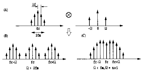
[Third Embodiment of the Optical-Spectrum Flattening Apparatus]
FIG. 9 shows the configuration of an apparatus for realizing
the optical-spectrum flattening apparatus according to the
third embodiment of the present invention. In this optical-
spectrum flattening apparatus, means for generating a discrete
optical spectrum with a fixed correlationship applied to the
phases of the modes thereof is composed of the CW light source
201 and a phase modulator 233. Further, means for sifting the
discrete optical spectrum on the frequency axis is composed of
the amplitude modulator 203 synchronizing with the oscillator
202.
[Fourth Embodiment of the Optical-Spectrum Flattening
Apparatus]
FIG. 10 shows the configuration of an apparatus for
realizing the optical-spectrum flattening apparatus according
to the fourth embodiment of the present invention. In this
optical-spectrum flattening apparatus, the means for sifting
a discrete optical spectrum on the frequency axis is composed
of the phase modulator 233 synchronizing with the oscillator
202. The remaining part of the configuration is similar to that
in the third embodiment in FIG. 9.
[Fifth Embodiment of the Optical-Spectrum Flattening Apparatus]
FIG. 11 shows the configuration of an apparatus for
- 22 -
CA 02487177 2001-07-05
realizing the optical-spectrum flattening apparatus according
to the fifth embodiment of the present invention. As means for
controlling a shift in a discrete optical spectrum, this
optical-spectrum flattening apparatus has a multiplier (or
divider) 243 for multiplying (or dividing) the frequency of a
driving signal output from the oscillator 202. A modulator 245
controls the frequency shift amount of the discrete optical
spectrum depending on the multiplied (or divided) frequency from
the multiplier (or divider) 243.
A modulator 244 located before the multiplier (divider) 243
as means for generating a discrete optical spectrum with a fixed
correlationship applied to the phases of the modes thereof is
the amplitude modulator 203 in FIG. 6 or 8 or the phase modulator
223 or 233 in FIG. 9 or 10, respectively. The modulator 245
located after the multiplier (divider) 243 as means for sifting
the discrete optical spectrum is the amplitude modulator 204
in FIG. 6 or 9 or the phase modulator in FIG. 8.
[Sixth Embodiment of the Optical-Spectrum Flattening Apparatus)
FIG. 12 shows the configuration of an apparatus for
realizing the optical-spectrum flattening apparatus according
to the sixth embodiment of the present invention . As means for
controlling the frequency shift amount of a discrete optical
spectrum, this optical-spectrum flattening apparatus has the
phase modulator 214 for counting the modulation index for phase
modulations. For wide-band phase modulations having a fixed
modulation index or more, the phase modulator 214 generates a
higher sideband to provide a larger frequency shift amount . The
remaining part of the configuration is similar to that in the
third embodiment in FIG. 9.
- 23 -
CA 02487177 2001-07-05
[Seventh Embodiment of the Optical-Spectrum Flattening
Apparatus]
FIG. 13 shows the configuration of an apparatus for
realizing the optical-spectrum flattening apparatus according
to the seventh embodiment of the present invention. This
optical-spectrum flattening apparatus is characterized by
having a phase adjuster 255 for controlling the phase of a driving
signal from the oscillator 202 , as means for controlling level
deviations among the modes of a discrete optical spectrum. The
driving signal having its phase controlled by the phase adjuster
255 is provided for the amplitude modulator 204. The remaining
part of the configuration is similar to that in the third
embodiment in FIG. 9.
By way of example, a description will be given of a case
in which a discrete optical spectrum obtained by modulating the
phase of a CW light to apply a fixed correlationship to the phases
of its modes has its amplitude modulated. For simplicity, it
is assumed that the driving signal from the oscillator 202 is
a sinusoidal wave; this sinusoidal wave, provided for the
amplitude modulator 204 , has its phase controlled by the phase
adjuster 255. In this case, it is assumed that the driving
signal to the phase modulator 204 has its amplitude modulated
by advancing the phase by 8 . An output waveform from the phase
modulator 223 is given by the following equation:
fpm( t ) - cos ( 2nfct + mcos2nOft ) ( 10 )
where fc represents a carrier frequency, 0 f represents a
modulated frequency, and m represents a modulation index.
- 24 -
CA 02487177 2001-07-05
Further, a temporal waveform from the amplitude modulator
204 is given by the following equation:
m(t) - A(1+cos(2nOft+ 8)) (11)
Thus , the f inal output is given by the following equation
f(t) - fpm(t) x fam(t) (12)
In this case, when spectra of the waveforms fpm( t ) and fam( t )
are defined as Fpm(f) and Fam(f), a spectrum F(f) is given by
the following equation:
F(f) - [Fpm(f)*Fam(f) ] (13)
where * represents convolution.
F(f) - ~Jn(m)8(f-fc-n~f)
(n = 0, ~1, t2, ...) (14)
where E represents the sum of n - 0 , t 1, ~ 2 , t 3 , . . . ~ ~ .
Further, Jn denotes Bessel functions of the order n.
For simplicity, it is assumed that in the case of narrow-band
modulations for m « 1, ~ n ~ = 3 or more is negligible . The phases
of the modes are shown below.
J o(m)JO = Ate(+jmcos6/2]
J+1(m)J+1 - An[cos9+j(m+sin0)]/2
J_1(m)J-1 - An(cos6+j(m-sinA)]/2
- 25 -
CA 02487177 2001-07-05
J+2 ( m ) J+2 - Aarmexp j ( 6+n/ 2 ) / 4
J_2(m)J-2 - Anmexp-j(6-n/2)/4
(15)
In this manner, the amplitude of each mode depends on a phase
shift of zero, as shown in FIG. 14.
Thus, level deviations among the modes can be controlled
by the phase adjuster 255 by varying the value of 8, FIG. 15
shows the case of B - 0, n/2, and -n/2.
In this embodiment , the phase modulator 223 is shown as the
means for applying the fixed correlationship to the phases of
the modes of the discrete optical spectrum, and the amplitude
modulator 204 is shown as the means for sifting the spectrum,
but level deviations among the modes can be controlled as
described above, using the reverse configuration in which the
amplitude modulator is used as the means for generating a
discrete optical spectrum, while the phase modulator is used
as the means for sifting the spectrum.
[Eighth Embodiment of the Optical-Spectrum Flattening
Apparatus]
FIG. 16 shows the configuration of an apparatus for
realizing the optical-spectrum flattening apparatus according
to the eighth embodiment of the present invention. This
optical-spectrum flattening apparatus is composed of a
repetition pulsed light source 302 having the central frequency
fc and driven by a sinusoidal signal of the frequency D f output
from an oscillator 301, and a modulator 303 synchronizing with
the oscillator 301 to modulate the amplitude or phase. In
general, an optical-pulse train output at a certain pulse
- 26 -
CA 02487177 2001-07-05
repetition frequency D f has a discrete optical spectrum of a
mode spacing 0f which has a fixed correlationship among the
phases of the modes thereof . The spectrum can be flattened by
using the modulator 303 to modulate with a frequency SZ ( SZ= 0
f in Fig. 18 and 19), an optical pulse of the central frequency
fc from the repetition pulsed light source 302, thereby shifting
the spectrum to sidebands occurred by the modulation, so that
the spectra shifted to the upper and lower sidebands overlap
each other.
When temporal deviations in the envelope of an optical pulse
are assumed to be sufficiently slow compared to the period of
the light , the field amplitude E ( z , t ) of the optical pulse is
given by the following equation:
E(z,t) - Re{U(z,t)exp-i(2nfct+8o)} (16)
The envelope of the optical pulse is given by the following
equation:
U(z,t) - ~U(z,t)lexp{-i8(z,t)} (17)
where fc denotes the central frequency and 8 o denotes an initial
phase.
First, amplitude modulations will be considered as means
for carrying out the above described second process. In this
case, B(z, t) - 8'. When the amplitude is modulated using a
sinusoidal signal V ( t ) = cos ( 2 TC S2 t ) of the frequency SZ and the
modulation index m, an amplitude-modulated wave M(t) is given
by the following equation:
- 27 -
CA 02487177 2001-07-05
Mam(t) - Re[+mv(t)]E(z,t)
- Re [ +mcos ( 2~S2t ) ] ~U ( z , t ) ~exp{ -i ( 2xfct+8' +80 ) }
- ~U( ( z , t ) ) ~cos{ 2~fct+8' +80 ) }
+m~U ( z , t ) ~cos { 2~ ( f c+S2 ) t+8' +80 ) / 2
+mIU(z,t)~cos{2~t(fc-SZ)t+8'+80)/2 (18)
In this case, the spectrum is sifted to the sidebands ( fc
~ S2 ) based on the frequency shifting theorem. When the spectrum
of the optical-pulse is 2fm in width, the following relationship
must be met in order to allow the sifted spectra to overlap each
other:
S2 < 2fm (19)
When this condition is met , the shifted spectra overlap each
other, thus obtaining a flattened wide-band optical spectrum.
Further, a spectrum of an optical pulse of the pulse
repetition frequency D f undergoes mode oscillation at intervals
of 0 f , so that the frequency shift SZ must equal the frequency
D f or must be a multiple thereof in order to allow the modes
to overlap each other.
S2 = n x ~f( n: natural number) (20)
This condition can be met by synchronizing the oscillator
for driving the repetition pulsed light source (or optical-
pulse generating circuit ) 302 , with the oscillator for driving
the modulator 303, and multiplying the driving signal from the
- 28 -
CA 02487177 2001-07-05
multiplier (not shown) to the modulator 303 as required.
The use of a phase (frequency) modulator as the modulator
303 will be described below. As described above, when the
amplitude is modulated using the sinusoidal signal V ( t ) = cos ( 2
TC 0 f t ) of the frequency S2 ( S~ = 0 f ) and the modulation index m,
an amplitude-modulated wave Mpm(t) is given by the following
equation:
Mpm(t) - Re{~U((z,t)~exp-i(2nfct+mv(t)+6o)}
- ~U(z,t)~exp{-i(2nfct+mcos(2nOf)+8(z,t)+8o)}
- ~U ( ( Z , t ) ) ~~Jn ( m ) cos { 2n ( f c+nOf ) t+
8(z,t)+nn/2+Ao}
(21)
The equation (18) indicates that the phase modulation
infinitely generates an upper and lower sidebands of a magnitude
Jn ( m ) at locat ions f c t n 0 f . In this case , the spectrum of the
optical pulse shifts to the upper and lower sidebands
corresponding to index m ( the larger m is , the greater a frequency
shift amount is), the resulting spectrum comprises the
overlapping spectra, which have been shifted to the locations
of the upper and lower sidebands.
We described above on SZ = D f ( n : natural number ) . In order
for overlapping of respective modes, however, due to the
generating mode oscillation by intervals 0 f with the spectrum
of the optical pulse, S~ value is required to be equal to n x
D f as well as equation (20). Furthermore, when the spectrum
of the optical-pulse is 2fm in width, ~2 value is required to
satisfy 2 fm < ~ in order for overlapping of sifted spectrum
- 29 -
CA 02487177 2001-07-05
as well as the second embodiment.
As described above, a flattened wide-band spectrum can be
obtained by modulating the amplitude or phase of a pulsed light
of the pulse repetition frequency D f with the frequency S2 -
n x 0 f to shift the spectrum to the sidebands occurred by the
modulation thereby allow the optical spectra obtained to overlap
each other.
The above operation according to this embodiment generates
a repetition pulse from the repetition pulsed light source 302
and generates discrete modes with the ffixed correlationship
applied to the phases. Controlling the power level deviations
among the modes can be accomplished by sifting these longitudinal
modes by a distance corresponding to the modulating frequency
or the modulation index so as to overlap each other by modulating
operation of the modulator 303.
[Ninth Embodiment of the Optical-Spectrum Flattening Apparatus)
FIG. 17 shows the configuration of an apparatus for
realizing the optical-spectrum flattening apparatus according
to the ninth embodiment of the present invention. This
optical-spectrum flattening apparatus is composed of the
repetition pulsed light source 302 for outputting an optical
pulse at the frequency D f provided by the oscillator 301, a pulse
expander 314 for expanding the optical pulse output from the
repetition pulsed light source 302, and a amplitude modulator
315 for modulating the optical pulse output from the pulse
expander 314 using a multiplying frequency output from a
multiplier 313. The pulse expander 314 may comprise a
dispersive medium such as a single-mode fiber or a dispersive
optical-function circuit.
- 30 -
CA 02487177 2001-07-05
In the optical-spectrum flattening apparatus of the above
described eighth embodiment, the modulating frequency requires
a band of about 1 THz ( 100 times as wide as the pulse repetition
frequency) in order to carry out the above second process on
a short optical repetition pulse, particularly, a short optical
pulse having a repetition rate of lOGHz and a pulse width of
about several tens of psec (that is, its spectrum has a wide
band) . Thus, when the pulse width t0 and the pulse repetition
frequency D f have a relationship t0 « ( 1/ d f ) , since the current
electric circuits have a modulating band of several tens of GHz ,
it is technically very difficult to execute the above second
process. In contrast, the optical-spectrum flattening
apparatus of this embodiment provides the means for expanding
the pulse width (or full width at half maximum) of the optical
pulse during the first process, thus reducing the modulating
frequency for the second process. In this case, a relationship
D f ~ SZ must be established between the pulse recurrent
frequency 0 f and the modulating frequency SZ .
In particular, when the dispersive medium such as a
single-mode fiber is used in the pulse expander 314 to expand
the pulse width, linear chirp is applied to the optical pulse
to expand the pulse width.
A temporally resolved spectral image output from the
repetition pulsed light source 302 is shown in FIG. 18. When
this optical pulse is passed through the dispersive medium of
the pulse expander 314 , the linear chirp is applied to the optical
pulse to expand the pulse width (or full width at half maximum)
of the pulse, as shown in FIG. 19.
The multiplier 313 multiplies a sinusoidal electric signal
- 31 -
CA 02487177 2001-07-05
of the pulse repetition frequency 0 f from the oscillator 301
by n to produce an electric signal of frequency n X 0 f. The
electric signal drives the amplitude modulator 315 to vary the
phase of the optical pulse transmitted through the dispersive
medium of the pulse expander 314 , the optical pulse having been
subjected to the linear chirp. At this time the temporal
waveform of the optical pulse can have its amplitude modulated
as shown in FIG. 20.
Further, power level deviations among the modes can be
restrained by varying the waveform of the signal output from
the oscillator 301, the modulation index for this signal, or
the phase thereof.
[Tenth Embodiment of the Optical-Spectrum Flattening Apparatus]
FIG. 21 shows the configuration of an apparatus for
realizing the optical-spectrum flattening apparatus according
to the tenth embodiment of the present invention. This
optical-spectrum flattening apparatus is obtained by replacing
an optical amplifier 325 for the amplitude modulator 315 varying
the amplitude of an optical spectrum with its shape manipulated
according to the above ninth embodiment . The other components
of this configuration are similar to those of the configuration
in FIG. 17.
The optical-spectrum shape manipulating method according
to this embodiment allows the shape of a spectrum to be
manipulated by causing the optical amplifier 325 to vary the
amplitude on the time axis, as in the optical-spectrum shape
manipulating method in the above described ninth embodiment.
Further, in this embodiment, since the optical amplifier
325 is used as the means for varying the amplitude, the optical
- 32 -
CA 02487177 2001-07-05
spectrum can be flattened while restraining energy losses from
the pulse.
More specifically, in the optical-spectrum shape
manipulating method according to this embodiment , a chirp pulse
resulting from transmission through the linear medium of the
pulse expander 314 is input to the optical amplifier 325, which
is in a saturated area. The optical amplifier 325 in the
saturated area provides a large gain for low power, while
providing a small gain for high power, as shown in FIG. 22. Thus,
as shown in the left of FIG. 23, the gain is large at a rising
and a falling edge of the temporal waveform of the chirp pulse,
but is small near the center of the pulse . As a result , as shown
in the right of FIG. 23, the optical pulse has a rectangular
waveform and is flattened.
As described above, according to this embodiment, when the
temporal waveform of the chirp pulse is manipulated, the optical
pulse can be flattened while restraining power losses from the
pulse. In particular, if the pulse expander 314 comprises a
medium for providing a saturated output, and if the optical pulse
is input to the gain saturated area of the optical amplifier
325, an optical-spectrum flattening apparatus with reduced
pulse power losses can be configured.
The pulsed light source 302 or the optical-pulse output
circuit may typically comprise a semiconductor- or fiber-
ring-type active/passive mode lock laser.
[Eleventh Embodiment of the Optical-Spectrum Flattening
Apparatus]
FIG. 24 shows the configuration of an apparatus for
realizing the optical-spectrum flattening apparatus according
- 33 -
CA 02487177 2001-07-05
to the eleventh embodiment of the present invention. This
optical-spectrum flattening apparatus can shift the phase of
a modulated signal output from the oscillator 301, by using a
phase adjuster 333 for the means for modulating the amplitude
of a pulse expanded by a dispersive medium 334. By providing
the amplitude modulator 315 with the driving signal with its
phase shifted, the amplitude modulator 315 can regulate the
flatness of the modulated optical spectrum depending on the phase
shif t .
[Flow of the Entire Process]
The flow chart in FIG. 25 generally shows a power level
deviation restraining method according to the above described
embodiment of the present invention.
First, at step S1, a CW light is modulated (amplitude or
phase) with the modulating frequency D f to output a discrete
optical spectrum with a fixed correlationship applied to the
phases of the modes thereof . The process proceeds to step S5 .
On the other hand, at step S2, a pulsed light source of the
pulse repetition frequency 0 f is used to output the discrete
optical spectrum with the fixed correlationship applied to the
phases of the modes thereof . It is then determined whether or
not the optical-pulse width (full width at half maximum) t0 «
( 1/ D f ) . If the result of the determination is affirmative, then
at the subsequent step S3, the pulse width is expanded, and the
process proceeds to step S4. On the other hand, if the result
of the determination is negative, the process immediately
proceeds to step S5. In the present invention, either the step
S1 or S2 may be used.
At the step S4, the above discrete optical spectrum is
- 34 -
CA 02487177 2001-07-05
modulated (amplitude or phase) with the modulating frequency
SZ to shift the discrete optical spectrum to an upper and lower
sidebands. Then, the process proceeds to the step S5.
At the step S5, level deviations among the modes are
restrained, and the following processing is executed:
(1) The modulating frequency is multiplied or divided.
(2) The modulation index is varied.
(3) The phase (timing) of the modulating signal is shifted.
As described above, according to the present invention, the
fixed correlationship is applied to the phases of the modes of
the discrete optical spectrum to shift the spectrum on the
frequency axis while controlling the frequency shift, thereby
providing a simple and inexpensive configuration and making it
possible to control ( restrain ) power level deviations among the
modes of the discrete optical spectrum.
In particular, according to the first aspect of the present
invention, the CW light source for outputting a continuous wave
at the fixed frequency fc output from the oscillator is used
and the continuous wave from the CW light source is modulated
with the frequency O f to generate the upper and lower sidebands
fc~n D f having the correlationship among the phases of the modes .
The amplitude or phase of this modulated wave is modulated again
with the frequency S2 to shift the discrete optical spectrum
to the locations of the upper and lower sidebands. At this time,
if the spectrum of the optical-pulse is 2fm in width, the modes
of the resulting optical spectra overlap each other when S2
2fm. Consequently, power level deviations among the modes can
be restrained.
Further, according to the second aspect of the present
- 35 -
CA 02487177 2001-07-05
invention, the repetition pulsed light source is used as the
means for applying the fixed relationship to the phases of the
modes of the discrete optical spectrum. In this case, when the
relationship t0 « (1/0 f) is established between the pulse
repetition frequency 0 f and pulse width ( or full width at half
maximum) of an output optical pulse train, the discrete optical
spectrum can be sifted to the upper and lower sidebands by means
of an amplitude or phase modulation after the pulse width has
been expanded. The above manipulation makes it possible to
relatively reduce the modulating frequency for very short
optical pulses of pulse width about 1 ps or less.
The basic principle of a multi-wavelength generating
apparatus according to another aspect of the present invention
will be described with reference to FIG. 26.
The present apparatus comprises a group of optical
modulators 2 having at least one optical modulators coupled
together in series and arranged at predetermined locations of
a plurality of optical paths including one to which an incident
light having a single central frequency is input , and a plurality
of power regulators 4 for independently regulating a signal
voltage of a predetermined period and applying the voltage to
an input port of each optical modulator. The light source 1
generates an incident light having the single central frequency.
The optical modulators can preferably modulate the amplitude
or phase of the incident light . The plurality of optical paths
in the group of optical modulators 2 may include paths coupled
together in parallel.
The output field E ~ t ) obtained when the amplitude and phase
of the incident light having the single central frequency are
- 36 -
CA 02487177 2001-07-05
modulated using functions a(t) and b(t) is expressed by:
E(t) - a(t)cos(w~t+b(t)) (22)
Thus , the shape of an output optical spectrum can be designed
in accordance with the functions a ( t ) and b ( t ) . In this equation,
w~ is the central angular frequency of the incident light having
the single central frequency, and t denotes the time.
In the present apparatus, the optical modulators capable
of modulating the amplitude and/or phase are arranged in a
modulating section at arbitrary locations of the optical paths
coupled together in series and/or parallel, and the power of
the signal voltage of the predetermined period applied to the
optical modulators constituting the group of optical modulators
is modulated to properly set the function a ( t ) for modulating
the amplitude of the incident light having the single central
frequency and/or the function b(t) for modulating the phase
thereof. Consequently, a generated output multi-wavelength
optical spectrum can be flattened.
Since the multiplicity of optical modulators are arranged,
the amplitude and phase can be modulated more freely, thus
improving the flatness of the output optical spectrum and
increasing the modulation depth to widen the band of the output
optical spectrum.
Subsequently, specific embodiments will be described,
[First Embodiment of the Multi-wavelength Generating Apparatus]
FIG. 27 shows the configuration of a first embodiment of
a multi-wavelength generating apparatus according to the
present invention.
- 37 -
CA 02487177 2001-07-05
As shown in FIG. 27, the multi-wavelength generating
apparatus of this embodiment is composed of the light source
1, the group of optical modulators (modulating section)
including n (~ 1) optical modulators, a repetition period
signal generator 3 , the n power regulators 4 , and n power-varying
DC power supply 5. The light source 1 generates a light having
a single central frequency, which then falls on the input-side
optical modulator of the group of optical modulators 2. The
optical modulators of the group 2 are arranged (in FIG. 27, in
series ) at arbitrary locations of the plurality of optical paths
coupled together in series and/or parallel, so as to modulate
the amplitude and/or phase of the incident light. The
output-side optical modulator outputs a multi-wavelength light.
The repetition period signal generator 3 generates a signal
voltage repeated at a predetermined period, so that this power
is applied to the optical modulators after being regulated by
the power regulator 4. The power-varying DC power supplies 5
are further coupled to the corresponding optical modulators as
required so as to apply a power-regulated bias thereto. The
optical modulators modulate the incident light on the basis of
the above signal voltage and bias , so as to modulate the amplitude
and/or phase of the incident light from the light source 1.
In this connection, an output optical spectrum extended to
both sides of a carrier frequency as a result of the phase
modulation has a small optical-power area in the vicinity of
the carrier frequency; the output optical spectrum can be
flattened by modulating the amplitude to apply a pulsed gate
to a temporal waveform to thereby increase the power of that
area. The flatness of the output optical spectrum is determined
- 38 -
CA 02487177 2001-07-05
by the relationship between the amount of phase modulation and
the temporal width of the pulse. In this embodiment, the
flatness is determined by causing the power regulator 4 to
regulate the signal voltage of the predetermined period applied
to the optical modulators and causing the power-varying DC power
supplies 5 to vary the bias applied to the optical modulators
in order to determine the above relationship.
The ability of the configuration of this embodiment to
flatten the output optical spectrum from the group of optical
modulators 2 will be described with reference to FIGS. 28 and
29.
The temporal waveform of the output signal voltage from the
repetition period signal generator 3 corresponds to an angular
function as shown as shown by Reference numeral (a) in FIG. 28.
When the light source light having the single central frequency
has its phase modulated in accordance with this function, the
resulting multi-wavelength output optical spectrum is as shown
by Reference numeral (b) in FIG. 28. This will be described
below.
The angular frequency of this phase modulation involves a
square wave that reciprocates with a predetermined period
between an instantaneous value com and an instantaneous value
- c,~m as shown by Reference numeral ( c ) in FIG . 28 . As shown by
the solid line indicated by Reference numeral (d) in FIG. 28,
when a portion of this square wave which has its angular frequency
represented by the instantaneous value c.~,~ is gated by a
repetition NRZ (Non Return to Zero) signal, the resulting optical
spectrum is as shown by Reference numeral (e) in FIG. 28; the
optical spectrum of the repetition NRZ signal having a central
- 39 -
CA 02487177 2001-07-05
angular frequency ( c,~ ~ + c.~ m ) is obtained . Moreover , as shown
by the solid line indicated by Reference numeral (f) in FIG.
28, when a portion of this square wave which has its angular
frequency represented by the instantaneous value -cum is
similarly gated, the resulting optical spectrum is as shown by
Reference numeral (g) in FIG. 28; the optical spectrum of the
repetition NRZ signal having a central angular frequency
- com) is obtained.
The overlap between these optical spectra on the
angular-frequency axis is as shown by reference numeral (b) in
FIG . 28 , which corresponds to the sum of FIG . ( a ) and ( g ) . The
optical-spectrum intensity is low in the vicinity of the
instantaneous value c,~~ (central frequency, that is, carrier
frequency) of the angular frequency, thus preventing the optical
spectrum from being flattened.
Thus , the spectrum is flattened as described below by means
of regulations using the power regulators 4 and the power-varying
DC power supplies 5.
An output optical spectrum will be considered which is
obtained through such regulations that the repetition NRZ signal
gates the square wave between the instantaneous values com and
- c,~m of the angular frequency as shown by reference numeral ( a )
in FIG. 29.
As described above, As shown by the solid line indicated
by reference numeral ( c ) in FIG . 29 , when a portion of the square
wave which has its angular frequency represented by the
instantaneous value c.~m is gated by a repetition RZ (Return to
Zero) signal, the resulting optical spectrum is as shown by
reference numeral (d) in FIG. 29; the optical spectrum of the
- 40 -
CA 02487177 2001-07-05
repetition RZ signal having a central angular frequency ( co~ +
c,~m) is obtained. Moreover, as shown by the solid line indicated
by reference numeral ( a ) in FIG . 29 , when a portion of the square
wave which has its angular frequency represented by the
instantaneous value -wm is similarly gated, the resulting
optical spectrum is as shown by reference numeral (f) in FIG.
29; the optical spectrum of the repetition RZ signal having a
central angular frequency ( co~ - com) is obtained. Both optical
spectra have a wider band than that of the repetition NRZ signal.
The overlap between these optical spectra on the
angular-frequency axis is as shown by reference numeral (b) in
FIG. 29, and the optical-spectrum intensity is high in the
vicinity of the angular frequency w~, thus providing a flattened
optical spectrum.
According to this embodiment , the amplitude and phase are
modulated by properly setting the functions for modulating the
amplitude and phase of the light source light having the single
central frequency, and correspondingly regulating the power of
the signal voltage and variably setting the bias. Consequently,
the flatness of the output optical spectrum can be improved with
the simple and inexpensive configuration.
[Variation of the First Embodiment of the Multi-wavelength
Generating Apparatus]
FIG. 30 shows the configuration of a deviation of the first
embodiment of the multi-wavelength generating apparatus
according to the present invention. As shown in FIG. 30, the
multi-wavelength generating apparatus of this deviation may
comprises optical amplifiers 50 arranged in an optical path to
which a multi-wavelength light is emitted by the light source
- 41 -
CA 02487177 2001-07-05
1. In this figure, the optical amplifiers 50 are arranged in
all the plural optical paths including the one to which an
incident light from the light source 1 is input . The amplified
gain of the optical amplifiers 50 arranged in this manner makes
it possible to compensate for a power loss resulting from the
passage of the incident light through the optical amplifiers
as well as a power loss per wavelength resulting from the multiple
wavelengths. This results considerably improved output SNR.
Provided, however, that an optical amplifier 50 is arranged
only after the group of optical modulators 2 having no optical
amplifier, a drop in SNR caused after the optical amplifier 50
by the loss of the optical power is prevented. When the optical
amplifiers 50 are added to all the plural optical paths as shown
in the figure, the SNR of the multi-wavelength light obtained
in the output can be improved.
Furthermore, if all the optical modulators of the group 2
are phase modulators , power level deviations among channels can
be restrained by setting the sum of sinusoidal signal voltages
at a value converted into a predetermined phase modulation index,
the sinusoidal signal voltages being generated by the repetition
period signal generator 4 and applied to the input ports of the
optical modulators.
FIG. 31 is a characteristic diagram showing an example in
which the power level deviations among the channels are varied
in such a deviation of the first embodiment.
FIG . 31 shows cases where the number of channels is 7 , 9 ,
or 11. For example , in the case of 7 channels , small power level
deviations of 5 to 6 dB can be achieved among the channels when
the sum of the sinusoidal signal voltages are regulated such
- 42 -
CA 02487177 2001-07-05
that their sum is approximately 1.0 n or 1.4n when it is
converted into a phase modulation index. In the case of 9 and
11 channels, the power level deviations among the channels
exhibit a substantially minimum value when similar regulating
values are used.
Reference numeral (a) in FIG. 29 for the first embodiment
shows a case where if the amplitude of the incident light having
its phase modulated using the angular modulating function is
gated, the spectrum is flattened by gating the amplitude at such
temporal intervals that the square wave covers each of the upper
angular portions . That is , in the first embodiment , if the wave
is composed of increase periods in which the phase of the incident
light with the single wavelength is modulated linearly with
respect to the signal voltage waveform applied to the input port
and in which the signal voltage increases monotonously during
a continuous period that is half of the period of the signal
voltage, and decrease periods each corresponding to the
remaining half continuous period and in which the signal voltage
decreases monotonously in such a manner that the monotonous
increase in the increase period and this monotonous decrease
are symmetrical, the signal voltage waveform is gated with such
timings shown by reference numeral (a) in FIG. 29 that the square
wave spans across the increase period (the differential
coefficient of the phase modulating function is positive ) and
the decrease period ( the differential coefficient of the phase
modulating function is negative).
In the deviation described here, the spectrum of the output
multi-wavelength light can also be flattened by gating the signal
voltage waveform individually during the increase periods and
- 43 -
CA 02487177 2001-07-05
during the decrease periods. This will be described with
reference to FIG. 32.
As already described (see (a) to (c) in FIG. 28), if the
incident light simply has its phase modulated using the angular
modulating function, the optical power decreases in the vicinity
of the carrier frequency, thus preventing the spectrum of the
output multi-wavelength light from being flattened.
Thus, in the deviation described here, the spectrum is
flattened as shown by reference numeral (b) in FIG. 32 by gating
the signal voltage waveform individually during the periods
(phase modulating function increase periods) when the
differential coefficient of the phase modulating function is
positive and during the periods (phase modulating function
decrease periods ) when the differential coefficient of the phase
modulating function is negative, as shown by reference numeral
(a) in FIG. 32.
The waveform shown by reference numeral (a) in FIG. 32 will
be considered by dividing it into ( c ) and ( a ) in FIG . 32 . The
gating operation with the waveform shown by reference numeral
(c) in FIG. 32 results in an RZ signal spectrum around the
instantaneous angular frequency ( c~~ + ce~m) as shown by reference
numeral ( d ) in FIG . 32 . The gating operation with the waveform
shown by reference numeral (e) in FIG. 32 results in an RZ signal
spectrum around the instantaneous angular frequency (w~ - t.~
m) as shown by reference numeral (f) in FIG. 32. Consequently,
these overlaps indicate that the spectrum of the output
multi-wavelength light can also be flattened as in the above
first embodiment by executing the gating with the waveform shown
by reference numeral (a) in FIG. 32.
- 44 -
CA 02487177 2001-07-05
Furthermore, another temporal waveform can be used as a
modulating function. For example, the temporal waveform may be,
for example, that of a sinusoidal wave that monotonously repeats
increasing and decreasing with a fixed period.
[Second Embodiment of the Multi-wavelength Generating
Apparatus]
The second embodiment of the multi-wavelength generating
apparatus according to the present invention includes an
amplitude modulating section 25 in which optical paths coupled
together in parallel are provided in a group of optical
modulators 2a, with at least one of the optical paths having
one of the optical modulators arranged therein, as shown in FIG.
33 ( in FIG . 33 , all the optical paths coupled together in parallel
have the optical modulator arranged therein). The amplitude
modulating section 25 has an input-side optical modulator and
an output-side optical modulator coupled thereto in series via
the optical path. The optical modulators themselves are phase
modulators, but the optical paths (optical modulators) can
cooperate with one another to operate as an amplitude modulator;
modulating operations are performed on the basis of a
power-regulated signal voltage and a power-varied bias.
[Third Embodiment of the Multi-wavelength Generating Apparatus]
FIG. 34 shows the configuration of the third embodiment of
the multi-wavelength generating apparatus according to the
present invention.
As shown in FIG. 34, the multi-wavelength generating
apparatus of this embodiment is composed of the light source
1 generating a light having a single central wavelength, a
bipolar Mach-Zehnder intensity modulator 20, a oscillator 3 for
- 45 -
CA 02487177 2001-07-05
generating a signal voltage repeated with a predetermined period,
the power regulator 4 , the power-varying DC power supply 5 , and
a phase adjuster 6. The power regulator 4 and the phase
regulator 6 are coupled together in series.
The bipolar Mach-Zehnder intensity modulator 20 has such
a well-known configuration that an incident light is branched
into two optical paths so that output lights from the optical
modulators arranged in the corresponding optical paths are
multiplexed and converged for emission. Each of the branched
paths has optical modulating means (phase modulating means)
arranged therein. These plural optical modulating means are
each a phase modulating means , but can cooperate with each other
in performing an amplitude modulating operation. Although the
optical modulating means may be provided in both the optical
paths , similar effects can be achieved by providing one of the
optical modulating means in only one of the optical paths.
A signal voltage from the oscillator 3 has its power
regulated properly by the power regulator 4 and is then applied
to one of the electrodes of the Mach-Zehnder intensity modulator
20. This signal voltage further has its temporal position
regulated by the phase regulator 6, has its power regulated
properly by the power regulator 4 , and is then applied to the
other electrode of the Mach-Zehnder intensity modulator 20 . The
latter electrode also receives a bias with its power regulated
properly, from the power-varying DC power supply 5.
A light from the light source 1 is incident on the
Mach-Zehnder intensity modulator 20. The Mach-Zehnder
intensity modulator 20 modulates the incident light on the basis
of the above signal voltage and bias; the amplitude and/or phase
- 46 -
CA 02487177 2001-07-05
of the light source light is modulated,
In this embodiment, the Mach-Zehnder intensity modulator
20 has a simple configuration due to its effect of simultaneously
modulating the amplitude and phase by properly regulating the
power of the signal voltage applied via the power regulator 4
and the bias applied by the power-varying DC power supply 5.
[Fourth Embodiment of the Multi-wavelength Generating
Apparatus]
FIG. 35 shows the configuration of the fourth embodiment
of the multi-wavelength generating apparatus according to the
present invention.
The multi-wavelength generating apparatus of this
embodiment shown in FIG. 35 comprises, instead of the oscillator
3 of the third embodiment, an oscillator 3a for generating a
sinusoidal signal voltage as one for generating a signal voltage
repeated with a predetermined period. It further comprises a
multiplier 7 coupled to the power regulator 4 in series.
This configuration varies the frequency of the signal
voltage applied to the opposite electrodes of the Mach-Zehnder
intensity modulator 20. That is, an output signal voltage from
the oscillator 3a is applied to one of the electrodes after having
its frequency multiplied by the multiplier 7, while the output
frequency from the oscillator 3a is applied to the other
electrode as it is.
In this embodiment, the signal voltage repeated with the
predetermined period and applied to the Mach-Zehnder intensity
modulator 20 is a sinusoidal signal of a single frequency, so
that the frequency band required for the electric elements
constituting the electric circuit (the phase modulator 6 and
- 47 -
CA 02487177 2001-07-05
the following component ) can be limited, thus reducing the costs
of these electric elements. Further, since the multiplier 7
multiplies the frequency of the signal voltage, the output
optical spectrum can have a wide band.
[Fifth Embodiment of the Multi-wavelength Generating Apparatus
FIG. 36 shows the configuration of the fifth embodiment of
the multi-wavelength generating apparatus according to the
present invention.
The multi-wavelength generating apparatus of this embodiment
shown in FIG. 36 is composed of the light source 1 generating
a light having a single central wavelength, a group of optical
modulators 2c consisting of the bipolar Mach-Zehnder intensity
modulator 20 and a phase adjuster 28 coupled together in series,
the oscillator 3 for generating a signal voltage repeated with
a predetermined period, the power regulator 4 , the power-varying
DC power supply 5, and the phase regulator 6.
A signal voltage from the oscillator 3 has its power regulated
properly by the power regulator 4 and is then applied to the
Mach-Zehnder intensity modulator 20. This signal voltage
further has its temporal position regulated by the phase
regulator 6, has its power regulated properly by the power
regulator 4, and is then applied to the Mach-Zehnder intensity
modulator 20. The Mach-Zehnder intensity modulator 20 also
receives a bias with its power regulated properly, from the
power-varying DC power supply 5.
A light from the light source 1 is incident on the group
of optical modulators 2c. The group of optical modulators 2c
modulate the incident light on the basis of the above signal
voltage and bias; the amplitude and/or phase of the light source
- 48 -
CA 02487177 2001-07-05
light is modulated.
In this embodiment, since the two optical modulators
(Mach-Zehnder intensity modulator 20 and phase adjuster 28 ) are
arranged in series , the output optical spectrum can have a winder
band than in the third and fourth embodiments.
FIG. 37 shows the results of an experiment according to this
embodiment in which a 10-GHz sinusoidal wave is used as the signal
voltage from the oscillator 3 which is repeated with the
predetermined period. FIG. 37 indicates that a flatness below
3dB can be achieved for a 9-channel signal including the central
frequency of the light from the light source 1.
[Sixth Embodiment of the Multi-wavelength Generating Apparatus]
In the sixth embodiment of the multi-wavelength generating
apparatus according to the present invention, the Mach-Zehnder
intensity modulator 20 and the phase adjuster 28 of the fifth
embodiment are replaced with each other as shown in FIG. 38.
This embodiment can perform modulating operations similar to
those of the f if th embodiment .
As shown in this example, even if the optical modulators
coupled together in series in the multi-wavelength generating
apparatus of the present invention are replaced with each other,
the output optical spectrum obtained is not affected, but effects
similar to those of the above embodiments can be obtained.
[Seventh Embodiment of the Multi-wavelength Generating
Apparatus]
In the seventh embodiment of the multi-wavelength
generating apparatus according to the present invention, the
Mach-Zehnder intensity modulator 20 of the fifth embodiment is
replaced with a group of optical modulators 2e comprising an
- 49 -
CA 02487177 2001-07-05
electro-absorption intensity modulators 200 as shown in FIG.
39. The multi-wavelength generating apparatus of this
embodiment provides operational effects similar to those of the
fifth embodiment as shown below.
FIG. 40 shows the results of an experiment according to this
embodiment in which a ZO-GHz sinusoidal wave is used as the signal
voltage from the oscillator 3 which is repeated with the
predetermined period. FIG. 40 indicates that a flatness below
3dB can be achieved for a 9-channel signal including the central
frequency of the light from the light source 1 as in the fifth
embodiment (FIG. 37).
[Eighth Embodiment of the Multi-wavelength Generating
Apparatus]
In the eighth embodiment of the multi-wavelength generating
apparatus according to the present invention, a phase adjuster
28a is provided after the group of optical modulators 2c of the
fifth embodiment, and the power regulator 4 and the phase
regulator 6 coupled together in series are correspondingly added,
as shown in FIG. 4Z. That is, this embodiment comprises the
group of three optical modulators; the first is an amplitude
modulator, and the second and third are phase modulators.
Thus , the output optical spectrum can have a much Wider band
than in the fifth to seventh embodiments.
[Ninth Embodiment of the Multi-wavelength Generating Apparatus]
In the ninth embodiment of the multi-wavelength generating
apparatus according to the present invention, an optical
branching unit 8 is arranged between the light source 1 and the
Mach-Zehnder intensity modulater 20 of the fifth embodiment,
an optical branching unit 9 is arranged between the Mach-Zehnder
- 50 -
CA 02487177 2001-07-05
intensity modulater 20 and the phase adjuster 28 of the fifth
embodiment, with the optical branching units 8 and 9 coupled
together, and a cascade circuit of a photoelectric converter
10, an arithmetic'unit 11, and a controller 12 is coupled to
a branching output of the optical branching unit 8, as shown
in FIG. 42. That is, this embodiment comprises the optical
branching units 8 and 9 at the input and output sides of the
Mach-Zehnder intensity modulator 20, respectively. The
controller 12 controls the bias provided to the Mach-Zehnder
intensity circuit 20 by the power-varying DC power supply 5.
In the above configuration, a branched light obtained with
the optical branching unit 8 by branching a light from the light
source 1 is allowed to fall on the output-side optical branching
unit 9 , and is transmitted therethrough in the direction opposite
to that of the output multi-wavelength light, and then falls
on the Mach-Zehnder intensity modulator 20. The light
transmitted in the opposite direction has the same central
wavelength as well as a light from the light source, which is
incident on the Mach-Zehnder intensity modulator 20 and has the
single central wavelength. The light transmitted in the
opposite direction is taken out by the input-side optical
branching unit 8 and then falls on the photoelectric converter
10. The light is then converted by the photoelectric converter
10 into an electric signal depending on its monitored power.
The arithmetic unit 11 calculates a difference between the level
of the electric signal obtained by the conversion and a preset
target value . The controller 12 regulates an output power from
the power-varying DC power supply 5 on the basis of the result
of the calculation to control a bias point for the Mach-Zehnder
- 51 -
CA 02487177 2001-07-05
intensity modulator 20, thus flattening the output optical
spectrum.
Another configuration is possible wherein an optical
circulator (not shown) is installed after the input-side optical
branching unit 8 so that the function of branching the light
from the light source 1 is provided for the optical branching
unit 8 , while the function of taking out the light transmitted
in the opposite direction and allowing it to fall on the
photoelectric converter 10 is provided for the optical
circulator. Further, the output-side optical branching unit 9
may be an optical circulator.
[Tenth Embodiment of the Multi-wavelength Generating Apparatus]
In the tenth embodiment of the multi-wavelength generating
apparatus according to the present invention, the optical
branching unit 9 is arranged between the Mach-Zehnder intensity
circuit 20 and the phase adjuster 28 of the fifth embodiment,
and the cascade circuit of the photoelectric converter 10 , the
arithmetic unit 11, and the controller 12 is coupled to an output
of the optical branching unit 9. That is, the Mach-Zehnder
intensity circuit 20 includes the optical branching unit 9 at
its output side . The controller 12 regulates the bias for the
Mach-Zehnder intensity modulator 20 provided by power-varying
DC power supply 5.
In the above configuration, an output light from the
Mach-Zehnder intensity modulator 20 which has been branched by
the optical branching unit 9 is output to the photoelectric
converter 10, where it is converted into an electric signal
depending on the monitored power of the light.
[Eleventh Embodiment of the Multi-wavelength Generating
- 52 -
CA 02487177 2001-07-05
Apparatus]
FIG. 44 is a view showing an eleventh embodiment of the
multi-wavelength generating apparatus according to the present
invention.
The above described ninth and tenth embodiments suffer from
a deviation in a target bias value due to a power deviation of
the light source 1. The eleventh embodiment would eliminate the
power deviation detriment.
The configuration of the embodiment includes an optical
branching unit 8 and a photoelectric converter l0a provided at
output of the light source 1 additionally to the configuration
of the tenth embodiment. The arithmetic unit 11 monitors an
input optical power level and an output optical power level of
the Mach-Zehnder intensity modulator 20 through the
photoelectric converters l0a and lOb. The controller 12
controls the power-varying DC power supplies 5 according to
monitored two levels such that a bias applied to the Mach-Zehnder
intensity modulator 20 by the power-varying DC power supplies
5 maintains the ratio of both optical power level constant . In
the eleventh embodiment , thus , the power deviation of the light
source 1 does not influence to the target bias value.
[Twelfth Embodiment of the Multi-wavelength Generating
Apparatus]
FIG. 45 is a view showing the configuration of the twelfth
embodiment of the multi-wavelength generating apparatus
according to the present invention.
In the multi-wavelength generating apparatus of this
embodiment , a light source light from 2n ( n is a natural number
of 1 or more) lasers for generating lights of different single
- 53 -
CA 02487177 2001-07-05
central wavelengths is divided into two beams, which are
separately processed. The results of the processes are
multiplexed to obtain a final multiplexed output. The
configuration and operation of this embodiment will be described
below in detail.
In FIG. 45, reference numerals 161, 162, 163, 16,, . . . 162n-1~
and 162" denote laser light emitting elements for generating
lights of different single central wavelengths, the elements
being arranged on the frequency axis at equal intervals in the
order of the subscripts. Reference numeral 1600 denotes an
optical multiplexes for multiplexing lights from odd-number-th
laser light-emitting elements. Reference numeral 1610 denotes
an optical multiplexes for multiplexing lights from even-
number-th laser light-emitting elements independently of the
odd-number-th laser light-emitting elements. The optical
multiplexers 1600 and 1610 may be optical couplers.
FIG. 46A shows the results of a measurement of an output
optical spectrum from the optical multiplexes 1600 when n = 8 ,
and FIG. 46B shows the results of a measurement of an output
optical spectrum from the optical multiplexes 1610 when n = 8.
These figures show that the eight light source lights are
arranged on the frequency axis at equal intervals . Further, the
powers of the light source lights are substantially the same.
One of the lights which is output from the optical
multiplexes and which has such a spectrum is incident on a
multi-wavelength generating apparatus (IM/PM) 1620, while the
other is incident on a multi-wavelength generating apparatus
(IM/PM) 1630 (IM/PM) 1630. The multi-wavelength generating
apparatuses 1620 and 1630 have a configuration similar to that
- 54 -
CA 02487177 2001-07-05
of the mufti-wavelength generating apparatus of the fifth
embodiment (see FIG. 36) and each comprise a group of optical
modulators composed of a Mach-Zehnder intensity modulator ( IM)
and a phase modulator(PM), a power regulator, a power-varying
DC power supply, and a phase regulator (see FIG. 36). Signal
voltages from the oscillators 1640 and 1650, which are repeated
within a predetermined period, are input to the mufti-wavelength
generating apparatuses 1620 and 1630, respectively, multi-
wavelength generating apparatus of a different configuration
such as the.ones disclosed in the first to tenth embodiments
may also be used.
Thus, the results of the measurement obtained when, for
example, n = 8 indicate that the output optical spectrum from
the mufti-wavelength generating apparatus 1620 is flattened as
shown in FIG. 47A and that the output optical spectrum from the
mufti-wavelength generating apparatus 1630 is flattened as
shown in FIG. 47B.
Then, a light output from the mufti-wavelength generating
apparatus 1620 is demultiplexed by a demultiplexer 1660 into
different wavelengths, which are then multiplexed by a
multiplexer 1680. Further, a light output from the multi-
wavelength generating apparatus 1630 is demultiplexed by a
demultiplexer 1670 into different wavelengths, which are then
multiplexed by a multiplexer 1690 . The lights obtained by means
of the multiplexing operations performed by both multiplexers
are mulitplexed by an optical coupler 1700.
If the lights shown in FIGS. 47A and 47B enter the
multiplexers 1660 and,1670, the results of a measurement of an
output optical spectrum from the optical coupler 1700 are as
- 55 -
CA 02487177 2001-07-05
shown in FIG. 48, and more WDM signals can be generated than
in the embodiments in which the light source light of the single
wavelength is modulated, thereby increasing the band of the
output optical spectrum.
[Modified Example of the Eleventh Embodiment of the Multi-
wavelength Generating Apparatus]
If multi-wavelength lights are obtained in the twelfth
embodiment, cross talk may disadvantageously occur between a
system composed of the elements 1600 to 1680 and a system composed
of the elements 1610 to 1690.
Thus, in this modified example, those side modes of the
modified outputs from the multi-wavelength generating
apparatuses 1620 and 1630 which are finally not used as signal
lights are deleted by a multiplexer and demultiplexer
(demultiplexer 1660 and multiplexer 1680 or demultiplexer 1670
and multiplexer 1690) by extracting central wavelengths emitted
from the laser light emitting elements 161, 163, ... 162n-1 and
162, 164, ... 162n, through output ports 171, 173, ... 172n_1 and
172, 174, ... 172n of the demultiplexers 1660 and 1670.
Consequently, when, for example, n = 8, lights free from
the areas shown by thick frames 181, 183, 185, and 18., in FIG.
47A are obtained at the output of the multiplexer 1680 . Further,
lights free from the areas shown by thick frames 182, 184, 186,
and 188 in FIG. 47A are obtained at the output of the multiplexes
1690. Since the optical power of these areas is zero at the
outputs of both multiplexers ( not shown ) , an optical output WDM
signal finally provided by the optical coupler 1700 by
multiplexing the lights is free from the cross talk between the
two systems.
- 56 -
CA 02487177 2001-07-05
As described above, this embodiment provides the
configuration comprising the modulating section having the at
least one optical modulating means coupled together in series
and arranged at the predetermined locations of the plurality
of paths including the one to which the incident light of the
single central wavelength is input , and the plurality of voltage
applying means for independently regulating and applying the
signal voltage of the predetermined period to the input port
of the optical modulating means. In this configuration, a
multi-wavelength light is generated by flattening the incident
light depending on the regulated and applied signal voltage and
the predetermined period of the signal voltage, thus making it
possible to generate a WDM signal as a multi-wavelength light
having a flattened optical spectrum, using the simple and
inexpensive configuration and without the need to design a
complicated optical circuit.
(Application of the Eleventh Embodiment of the Multi-wavelength
Generating Apparatus]
FIGS. 49A and 49B are schematic views useful in explaining
an applied operation of the twelfth embodiment of the
multi-wavelength generating apparatus according to the present
invention.
In the configuration shown in FIG. 45, the modulating
sections possessed by the multi-wavelength generating apparatus
1620 and 1630 are a first and a second modulating sections,
respectively. The wavelengths of lights incident on the
modulating sections are offset from each other by a distance
eight times as large as the intervals of the output multi-
wavelength light.
- 57 -
CA 02487177 2001-07-05
FIG. 49A is a schematic view showing the relationship
between both incident wavelengths in a case in which the
multi-wavelength generating apparatuses 1620 and 1630 generate
flattened 9-channel multi-wavelength lights and allow them to
fall on the first and second modulating sections . As is apparent
from this figure, the rightmost wavelength to the first
modulating section overlaps the leftmost wavelength to the
second modulating section, thus resulting in the useless
wavelengths.
Thus, in this applied example, the multi-wavelength
generating apparatuses 1620 and 1630 are operated independently
in such a manner that a flattened 9-channel multi-wavelength
light is allowed to fall on the first modulating section, whereas
a flattened 7-channel multi-wavelength light is allowed to fall
on the second modulating section. This operation can be
achieved by setting the voltages applied to the first and second
modulating sections at different values. Specifically, by
setting the voltage applied to the second modulating section
at a lower value than the voltage applied to the first modulating
section, the useless Wavelengths can be eliminated, while
reducing the signal voltage. Of course, similar effects are
obtained by reversing the operations of the first and second
modulating sections.
Next , several embodiments of another aspect of the present
invention will be described.
(First Embodiment of the Coherent Multi-wavelength Signal
Generating Apparatus)
FIG. 50 shows a first embodiment of a coherent multi-
wavelength signal generating apparatus. In this figure, the
- 58 -
CA 02487177 2001-07-05
coherent multi-wavelength signal generating apparatus is
composed of a multi-wavelength light source 311 of the above
embodiments, a demultiplexer 312 for slicing a spectrum of a
multi-wavelength light into different wavelengths, optical
modulators 352-1 to 352-n for modulating each spectrum-sliced
light using a transmitted signal, a multiplexes 353 for
multiplexing the modulated signal lights to output a coherent
multi-wavelength signal, an optical amplifier 354, an optical
coupler 355 for branching part of the multi-wavelength light
output from the multi-wavelength light source 311, and a control
circuit 350 for receiving the branched multi-wavelength light
and controlling the shape of the optical spectrum from the
multi-wavelength light source 311 so that the relative intensity
noise RIN for the inputs to the optical modulators or the
signal-to-noise ratio SNR for the outputs from the optical
modulators has a design value.
(Second Embodiment of the Coherent Multi-wavelength Signal
Generating Apparatus)
FIG. 51 shows the second embodiment of the coherent
multi-wavelength signal generating apparatus. The coherent
multi-wavelength signal generating apparatus of this embodiment
includes an optical amplifier 320 for amplifying a multi-
wavelength light which amplifier is arranged between the
multi-wavelength light source 311 and demultiplexer 312 of the
configuration of the first embodiment so that part of the
amplified multi-wavelength light is guided to the control
circuit 350.
FIG. 52 is an example of the configuration of a WDM
transmission system using the coherent multi-wavelength signal
- 59 -
CA 02487177 2001-07-05
generating apparatus of the present invention. In FIG. 52, an
optical receiving section 370 connected to a coherent
multi-wavelength signal generating apparatus 10 via an optical
amplifier 371 for amplifying a transmitted WDM (Wavelength
Division Multiplexing) signal light, a demultiplexer 372 for
demultiplexing the WDM signal light into signal lights of
different wavelengths, and receivers 373-I to 373-n for
receiving the corresponding signals lights of the different
wavelengths.
FIG. 53. is an example of a first configuration of a
multi-wavelength light source 311. In this figure, the
multi-wavelength light source 311 is composed of a light source
321 for generating a light of a single central wavelength, an
optical modulating section 323 having a plurality of optical
modulators 322-1 and 322-2 for modulating the amplitude or phase
of the optical light from the light source 321, a period signal
generator 324 for generating predetermined period signals,
power regulators 330-1 to 330-2 for regulating period signal
voltages to predetermined values and applying the obtained
voltages to the optical modulator 322-1 to 322-2, and
power-varying DC power supplies 326-1 to 326-2 for applying a
power-regulated bias voltage to each of the optical modulators
322-1 to 322-2. The optical modulating section 323 may be
configured to perform an amplitude modulating operation as a
whole by, for example, modulating the phase using a path branched
using a Mach-Zehnder intensity modulator.
FIG. 54 is a view useful in explaining the principle of
generation of a multi-wavelength light. The optical modulator
322-1 of the optical modulating section 323 modulates the
o _
CA 02487177 2001-07-05
amplitude or phase of the temporal waveform of an output light
(CW light) from the light source 311 to apply a fixed
correlationship to the phases of the modes of a discrete optical
spectrum of the output light (a). Furthermore, the optical
modulator 322-2 modulates the amplitude or phase of the modulated
wave to shif t the discrete optical spectrum to an upper and lower
sidebands on the frequency axis ( b ) . In this case , power level
deviations among the modes can be controlled to a fixed value
by regulating the frequency shift amount to cause the discrete
optical spectrum to overlap the upper and lower sidebands.
FIG. 55 shows an example of the shape of an optical spectrum
obtained if the optical modulating section 323 comprises an
intensity modulator and a phase modulator. Reference numerals
( a ) , ( b ) , and ( c ) in FIG . 55 show examples of spectra obtained
by varying the voltage ( V TC voltage ) applied to the Mach- Zehnder
intensity modulator, reference numerals (d), (e), and (f) in
FIG. 55 examples of spectra obtained by varying the voltage
( normalized by V n voltage ) applied to the phase modulator, and
reference numerals (g), (h), and (i) in FIG. 55 show examples
of spectra of multi-wavelength lights obtained when both
modulators are combined together for each applied voltage . The
optical spectra of the multi-wavelength lights each have a
plurality of carriers 341 as a coherent light and a spontaneous
emission light 342 extending over a wide band.
FIG. 56 is a schematic view of an optical spectrum of a
multi-wavelength light amplified by the optical amplifier. The
optical spectrum of the multi-wavelength light has the plurality
of carriers 341 as a coherent light, the spontaneous emission
light 342 extending over a wide band, and a spontaneous emission
- 6I -
CA 02487177 2001-07-05
light ( amplif ied spontaneous emission light : ASE ) generated by
the optical amplifier.
Control parameters for varying the shape of the optical
spectrum include the modulation index (period signal voltages)
for the intensity and phase modulators and the bias voltage for
the intensity modulator. That is, control can be provided so
as to obtain a predetermined optical spectrum by inputting
control signals to the power regulators 330-1 to 330-2 and the
power-varying DC power supplies 326-1 to 326-2 to thereby
regulate the period signal voltage and the bias voltage.
FIG. 57 shows an example of a second configuration of the
multi-wavelength light source 311. In this configuration, a
phase modulator 327 and a multiplier 328 are arranged before
the power regulators 330-1 to 330-2 of the example of the first
configuration. Control can be provided so as to obtain a
predetermined optical spectrum by causing the phase modulator
327 to regulate a phase difference between the period signals
applied to the optical modulators 322-1 and 322-2 and causing
the multiplier 328 to control the multiplier factors for the
frequencies of the period signals.
FIG. 58 is an example showing how the shape of an optical
spectrum is controlled by regulating the phase of the period
signal. Reference numerals (a), (b), and (c) in FIG. 58 show
the shapes of optical spectra obtained if the phase difference
is set at 0, +X, and -X.
FIG. 59 is an example showing how the shape of an optical
spectrum is controlled by multiplying the frequency of the period
signal. Reference numerals (a), (b), and (c) in FIG. 59 show
the shapes of optical spectra obtained if the multiplier factor
- 62 -
CA 02487177 2001-07-05
is set at 1, 2, and 3.
FIG. 60 shows an example of a third configuration of the
multi-wavelength light source 311. In this configuration, an
electro-absorption intensity modulator 329 is used as the
optical modulating section 323 of the example of the first
configuration . The shape of an optical spectrum can be varied
by utilizing the exponential characteristic of an absorption
factor (transmission factor.) for the voltage applied to the
electro-absorption intensity modulator to provide the period
l0 signal voltage with a rectangular output light intensity and
by varying the bias point to vary the duty ratio.
FIG. 61 is a schematic view of an optical spectrum of a
multi-wavelength light obtained if the electro-absorption
intensity modulator is used. The optical spectrum of the
multi-wavelength light has the plurality of carriers 341 as a
coherent light and the spontaneous emission light 342 extending
over a wide band.
FIG. 62 shows an example of a fourth configuration of the
multi-wavelength light source. In this figure, the multi-
20 wavelength light source 311 is composed of a pulsed light source
331 and spectrum shape control means 332 for controlling the
shape of a spectrum of an output pulsed light from the pulsed
light source 331. The spectrum shape control means 332 controls
the shape of a spectrum (relating to the pulse width and the
amount of chirp) in the frequency area of pulsed light to a
predetermined one by means of pulse compression such as adiabatic
compression using a dispersion reducing fiber. In this case,
the control parameter is a compression rate determined by a
dispersion value Do at the input side of the dispersion reducing
- 63 -
CA 02487177 2001-07-05
fiber and a dispersion value D1 at the output side thereof as
shown in FIGS. 63A to 63B.
FIG. 64 shows the relationship between an optical spectrum
of coherent components of a multi-wavelength light. In this
figure, a level 1 corresponds to the coherent components of the
multi-wavelength light, and the double of the level 2 or 3
corresponds to the noise of a beat frequency equal to the
wavelength channel spacing. Accordingly, if the transmission
band width for the demultiplexer 312 is sufficiently reduced
compared to the wavelength channel spacing of the multi-
wavelength light, then when a desired wavelength component is
cut out, leakage from the adjacent channels can be restrained.
This enables a CW light to be output even if the multi-wavelength
light is pulsed.
A description will be given of design for meeting a
performance specification required of a conventional optical
transmitting section using semiconductor lasers and which is
used in a structure for controlling the shape of an optical
spectrum of a multi-wavelength light.
(Example of Design of the Relative Intensity Noise RIN G) for
Inputs to the Modulator)
FIG. 65 shows the relationship between a stimulated
emission light and a spontaneous emission light from
semiconductor lasers. Below a threshold, the semiconductor
laser has its optical output intensity varying slowly with an
increase in injected current (excitation light intensity if
solid lasers are used), and at the threshold, it enters a
stimulated emission state to rapidly increase the optical output .
The spontaneous emission light is incoherent and is given as
- 64 -
CA 02487177 2001-07-05
an optical output intensity PS$, and the stimulated emission
light is coherent and is given as an optical output intensity
P~ depending on the injected current.
In this case, the stimulated emission probability ratio ?'
is defined by the following equation:
= lOloglo ( PLAS/PsE) ( 23 )
On the other hand, when the spontaneous output band is
ZO defined as BWSR[Hz], the relative intensity noise prior to
spectrum slicing by the multiplexes is defined as RIN[dB/Hz],
and the light intensity of the i-th wavelength component obtained
by the spectrum slicing by the multiplexes is defined as Pi,
the relative intensity noise RIN{ i ) is expressed by the following
equation:
RIN{i) - RIN+lOLoglo{Pi/~Pi)
RIN = -y-lOlogloBWs~+3 { 24 )
20 The control circuit 350 in FIG. 50 calculates the relative
intensity noise RIN G) of the i-th wavelength component by
measuring the relative intensity noise RIN of a mufti-wavelength
light and estimating the intensity Pi of the i-th output light
obtained by the spectrum slicing executed by the demultiplexer
312. Then, the power modulating section 330, power-varying DC
power supply 326 , phase regulator 327 , multiplier 328 , and others
of the mufti-wavelength light source 31I are controlled so as
to set the relative intensity noise RIN{i) of each wavelength
component at a design value.
- 65 -
CA 02487177 2001-07-05
Further, the intensity Pi of the i-th output Light, measured
using the input power monitoring function of the optical
modulators 352-I to 352-n, may be input to the control circuit
350 . Moreover, the control circuit 350 may directly measure the
relative intensity noise RIN G) of each wavelength component
obtained by the spectrum slicing executed by the demultiplexer.
Further, the multi-wavelength light amplified by the
optical amplifier 320 is input to the control circuit 350 in
FIG. 51. This multi-wavelength light has the spontaneous
emission light (amplified spontaneous emission light: ASE)
generated by the optical amplifier 320, as shown in FIG. 56.
If the gain of the optical amplifier 320 is defined as g,
the optical amplified area is defined as BW,,,,,~[Hz] , the total
number of lateral modes is defined as m, the population inversion
parameter is defined as ngp, and the central optical frequency
of the multi-wavelength light source 311 is defined as a[Hz],
then the ratio 7 of the probability of stimulated emission to
that of spontaneous emission is expressed by the following
equation:
y = lOloglo [ gPL,~~ { gPss ( BWsE~BW,~, ) +hv ( g-1 ) nsp~m~BW,~ } ]
(25)
( Example 1 of Design of the Signal-to-Noise Ratio SNR for Outputs
from the Modulator)
In the coherent multi-wavelength signal generating
apparatus shown in FIG. 50 or 51, the band of a receiver 373
of the WDM transmission system shown in FIG. 52 is defined as
Be[Hz], the demultiplexing band of the demultiplexer 372 is
- 66 -
CA 02487177 2001-07-05
defined as Bo [ Hz ] , the signal mark rate is defined as M, the signal
light intensity of an output from the i-th modulator is defined
as P(i)[dBm], the intensity of the stimulated emission light
in the output from this modulator is defined as Pc ( i ) [ dBm ] , the
intensity of the spontaneous emission light in the output from
this modulator is def fined as Ps ( i ) [ dBm] , an equivalent current
flowing through the receiver is defined as Ieq[A], shot noise
in the signal components is defined as Ns, the beat noise between
the signal components and the spontaneous emission light is
defined as Ns-sp, the beat noise between spontaneous emission
light is defined as Nsp-sp, and thermal noise from the receiver
is defined as Nth. Then, the signal-to-noise ratio SNR for
outputs from the modulators is expressed as follows:
SNR = S/(Ns~'Ns-sp-I-Nsp-sp-I-Nth)
Ps ( i ) - RIN ( i ) +lOlogloBe+Pc ( i ) +lOlogloM
S - ( (er~/hv)Pc(i) )z
Ns = 2e((e~/hv)P(i))Be
Ns-sp = 4(e~/hv)2Pc(i)Ps(i)Be/Bo
Nth = Ieq2Be
(26)
In this case, P(i), Pc(i), and Ps(i) in S, Ns, and Ns-sp
are expressed in W using the linear notation.
The control circuit 350 of the coherent multi-wavelength
signal generating apparatus controls the power modulating
section 330, power-varying DC power supply 326, phase regulator
327, multiplier 328, and others of the multi-wavelength light
source 311 so as to make the signal-to-noise ratio (SNR) for
- 67 -
CA 02487177 2001-07-05
outputs from the modulators follow the above equations.
(Example 2 of Design of the Signal-to-Noise Ratio SNR for Outputs
from the Modulator)
In the coherent multi-wavelength signal generating
apparatus shown in FIG. 50 or 51, the band of a receiver 373
of the WDM transmission system shown in FIG. 52 is defined as
Be[Hz], the demultiplexing band of the demultiplexer 372 is
defined as Bo[Hz ] , the signal mark rate is defined as M, the signal
light intensity of an output from the i-th modulator is defined
as P(i)[dBm], the intensity of the stimulated emission light
in the output from this modulator is defined as Pc ( i ) [ dBm] , the
intensity of the spontaneous emission light in the output from
this modulator is defined as Ps ( i ) [ dBm] , an equivalent current
flowing through the receiver is defined as Ieq[A] , the rate of
leakage from the j-th port to the i-th port of the multiplexer
is defined as XT( j ) , the light intensity of a cross talk signal
from the multiplexer is defined as Px(i)[dBm], shot noise in
the signal components is defined as Ns, the beat noise between
the signal components and the spontaneous emission light is
defined as Ns-sp, the beat noise between the signal components
and the cross talk signal light is defined as Ns-x, the beat
noise between spontaneous emission lights is defined as Nsp-sp,
the beat noise between the cross talk signal light and the
spontaneous emission light is defined as Nx-sp, and thermal noise
from the receiver is defined as Nth. Then, the signal-to-noise
ratio SNR for outputs from the modulators is expressed as
follows
SNR = S/(Ns~-Ns-sp'+"Nx-sp'~-Nsp-sp-~Ns-x'fNtn)
- 68 -
CA 02487177 2001-07-05
Ps ( i ) - RIN ( i ) +lOlogloBe+Pc ( i ) +101og1oM
Px(i) - EP(J)'XT(J)
S = ( (ey/hv)Pc(i) )z
Ns - 2e((e~/hv)P(i))Be
Ns-sp = 4(er~/hv)ZPc(i)Ps(i)Be/Bo
Nx-sp = 4(e~/hv)ZPx(i)Ps(i)Be/Bo
Ns-x = (er~/hv)2Pc(i)Px(i)
Nth = Ieq2Be
(27)
In this case, P(i), Pc(i), and Ps(i) in S, Ns, Ns-sp and
Ns-x are expressed in Ws using the linear notation.
The control circuit 350 of the coherent multi-wavelength
signal generating apparatus controls the power modulating
section 330 , power-varying DC power supply 326 , phase regulator
327, multiplier 328, and others of the multi-wavelength light
source 311 so as to make the signal-to-noise ratio (SNR) for
outputs from the modulators follow the above equations.
As described above, the coherent multi-wavelength signal
generating apparatus of the present invention is configured to
regulate the voltages or bias voltages of the period signals
applied to the optical modulators constituting the multi-
wavelength light source in order to control the shape of an
optical spectrum of a generated multi-wavelength light. This
makes it possible to quantitatively design the relative
intensity noise RIN for inputs to the optical modulators or the
signal-to-noise ratio SNR for outputs from the optical
modulators, the optical modulators modulating coherent lights
of different wavelengths obtained by slicing the spectrum of
- 69 -
CA 02487177 2001-07-05
the multi-wavelength light.
This also applies to the configuration for controlling the
shape of an optical spectrum of a multi-wavelength light
generated by controlling the phases of the period signals applied
to the optical modulators constituting the multi-wavelength
light source or the multiplier factors for the frequencies of
the period signals.
Consequently, a coherent multi-wavelength signal
generating apparatus can be designed which can meet the
performance specification required of the conventional optical
transmitting section using semiconductor lasers.
Next, several embodiments of yet another aspect of the
present invention will be described.
[First Embodiment of the Multi-wavelength Light Source]
FIG. 66 is a view showing the configuration of a first
embodiment of a multi-wavelength light source according to the
present invention.
In the multi-wavelength light source according to the
present invention, input lights from 2n (n is a natural number
of 1 or more ) light sources 4011 to 4102" are divided into two
lines, which are then multiplexed and modulated. The results
of the modulations are combined with orthogonal polarization
and then separated into a plurality of carriers of different
wavelengths to obtain the final output. The configuration and
operation of this embodiment will be described below in detail.
In FIG. 66, the light sources 410, 4102, 4103, . . . 4102n-1,
and 4102n comprise, for example, distributed feedback (DFB)
semiconductor lasers or external-cavity-type semiconductor
lasers. The light sources emit lights of different single
- 70 -
CA 02487177 2001-07-05
central wavelengths arranged on the frequency axis at equal
intervals in the order of the subscripts.
Reference numerals 421 and 422 denote optical multiplexers
comprising, for example, array waveguide diffraction gratings
or optical couplers; the optical multiplexer 421 multiplexes
lights from odd-number-th light sources. The optical
multiplexer 422 multiplexes lights from even-number-th light
sources independently of the multiplexer 421. A multiplexed
output from the optical multiplexer 421 is modulated by a
modulator 427, while a multiplexed output from the optical
multiplexer 422 is modulated by a modulator 428 . The modulators
427 and 428, for example, modifies the intensity and phase of
the input multiplexed light and are specifically one Mach-
Zehnder intensity modulator using lithium niobate as a medium
and one phase modulator using lithium niobate as a medium, the
modulators being connected together in series.
Output lights from the modulators 427 and 428 are combined
by the polarization multiplexer 430, and are demultiplexed into
different wavelengths by a demultiplexer 440 composed of a
separation filter, thus generating a plurality of optical
carriers of different wavelengths.
FIG. 67A shows an enlarged view of part of a multi-wavelength
optical spectrum of odd-number-th wavelengths at a goint A prior
to polarization multiplexing. FIG. 67B shows an enlarged view
of part of a multi-wavelength optical spectrum of even-number-th
wavelengths at a point B prior to the polarization multiplexing.
As shown in FIGS. 67A and 67B, the shape of a spectrum of
a side mode light from the modulator 427 (FIG. 67A) need not
necessarily be the same as the shape of a spectrum of a side
- 7i -
CA 02487177 2001-07-05
mode light from the modulator 428 ( FIG . 67B ) . These shapes may
be properly regulated after the polarization multiplexing by
the polarization multiplexer 430 so that the optical powers of
all the wavelengths are substantially the same as shown in FIG.
68. FIG. 68 shows an optical spectrum from a multi-wavelength
light source implemented with the above configuration including
2n = 32 light sources of wavelength spacing 100GHz, the spectrum
having been obtained at a point C before passage through the
final polarization multiplexer 430.
The number of wavelengths obtained after the wavelength
multiplexing process based on the present invention is generally
odd, but the system requirements often include an even multiple
of the number of light sources (for example, generation of
spectra at intervals of lOGHz, 12. SGHz, or 25GHz from a plurality
of light sources providing wavelengths at internals of 100GHz ) .
Thus, side mode lights are preferably generated by regulating
the operations of the modulators 427 and 428 so that, for example,
the wavelengths from the odd-number-th light sources are
multiplied by ( 2N + m ) ( N is a natural number, and m is an integer ) ,
whereas the wavelengths from the even-number-th light sources
are multiplied by (2N - m).
FIG. 67A shows an example in which the wavelengths from the
odd-number-th light sources are multiplied by 9. The
"multiplication by 9" means the light source wavelength shown
by an arrow 423 and eight other side mode lights, that is, the
optical powers of the nine wavelengths, are present within a
predetermined range. On the other hand, the example in FIG. 67B
shows, for the even-number-th light sources, "multiplication
by 7" in which the output powers of the light source wavelength
- 72 -
CA 02487177 2001-07-05
shown by an arrow 424 and of six other side mode lights are present
within a predetermined range . When the modulators 421 and 422
generate multi-wavelength lights of different spectral shapes
and the polarization multiplexer 430 combines these multi-
wavelength lights as described above, optical power deviations
among all the wavelengths can be reduced down to 3 . 5 dB or less ,
so that the optical powers are substantially uniform.
FIG. 69 shows the results of a measurement of the Q factor
of a signal obtained by causing a wavelength separating filter
of the demultiplexer 440 to separate the light source wavelengths
from one another and modulating each wavelength using a test
signal.
The Q factor is obtained by measuring the code error rate
by varying an identification point of a received waveform, while
measuring the code error rate, and by estimating a kind of
signal-to-noise ratio on the basis of the measurement. As the
Q factor increases, the signal-to-noise ratio increases and the
characteristics are improved. In FIG. 69, a light source
wavelength 443 and a light source wavelength 444 are obtained
from adjacent light sources (the subscripts of the reference
numerals are continuous). Polarization multiplexed
wavelengths side mode lights of the light source wavelengths
443 and 444 also exhibit high Q factors, indicating that this
embodiment enables signal modulation free from interfering
noise or the like.
[Second Embodiment of the Multi-wavelength Light Source]
FIG. 70 is a view showing the configuration of a second
embodiment of the multi-wavelength light source according to
the present invention.
- 73 -
CA 02487177 2001-07-05
The multi-wavelength light source according to this
embodiment is composed of light sources 4101 to 4102n, an optical
multiplexes 421, an optical multiplexes 422, a polarization
multiplexes 450, a modulator 455, and a demultiplexer 440.
Components denoted by the same reference numerals as those in
FIG. 66 have the same configuration, and description thereof
is thus omitted.
The multi-wavelength light source of this embodiment will
be described in comparison with that of the first embodiment.
In this embodiment, the polarization multiplexes 450 combines
a spectrum before the modulator 455 executes the wavelength
multiplexing process.
This configuration reduces the number of modulators, and
is thus much simpler than that of the first embodiment. The
modulator 455, however, must include a polarization-independent
intensity and phase modulators.
In the configuration of this embodiment, the modulator 455
preferably regulates the shape of a spectrum of side mode lights
generated by the light sources 4101 to 410zn so that the optical
powers of the wavelengths obtained at the point C before passage
through the polarization multiplexes 430 located at the end are
substantially equal.
An example of regulations will be described with reference
to FIG. 71, the regulations required if side mode light are
generated from a plurality of light sources providing
wavelengths at intervals of 100 GHz so that the spectrum spacing
is 12. 5 GHz after the wavelength multiplexing process according
to this configuration. Reference numerals (a) to (c) in FIG.
71 show spectra obtained at the point C. Numeral (a) shows a
- 74 -
CA 02487177 2001-07-05
spectrum from the odd-number-th light sources , numeral ( b ) shows
a spectrum from the even-number-th light sources; and numeral
(c) shows a combination of these spectra.
The spectrum from the odd-number-th light sources includes
a wavelength 461 from an odd-number-th light source, 6 side mode
lights 46Ia of a substantially equal power, and the other side
mode lights 461b of half the power, a wavelength 463 from another
odd-number-th light sources, 6 side mode lights 463a of a
substantially equal power, and the other side mode lights 463b
of half the power, . . . On the other hand, the spectrum from the
even-number-th light sources includes a wavelength 462 from an
even-number-th light source, 6 side mode lights 462a of a
substantially equal power, and the other side mode lights 462b
of half the power , . . .
When the intensity and phase modulating operations are
regulated so as to obtain such spectra, the optical spectrum
prior to separation is substantially uniform at the point C
before passage through the polarization multiplexer 430 located
at the end, as shown by numeral (c) in FIG. 71.
As described above, according to the multi-wavelength light
source of the present invention, when a plurality of optical
carriers are generated by generating side mode lights by means
of intensity and phase modulations to multiplex the wavelengths
of input lights from the plurality of light sources for
generating lights of different wavelengths, two side mode lights
of the same wavelength generated by different light sources with
contiguous wavelengths do not interfere with each other, thereby
preventing noise. A multi-wavelength light source having a
simple and inexpensive configuration and having no gap among
- 75 -
CA 02487177 2001-07-05
wavelength grids arranged at equal intervals can be provided
without the need to design a complicated optical circuit.
The present invention has been described in detail with
respect to preferred embodiments, and it will now be apparent
from the foregoing to those skilled in the art that changes and
modifications may be made without departing from the invention
in its broader aspect, and it is the intention, therefore, in
the apparent claims to cover all such changes and modifications
as fall within the true spirit of the invention.
- 76 -