Note : Les descriptions sont présentées dans la langue officielle dans laquelle elles ont été soumises.
CA 02487612 2004-11-10
FP03-0353-01
TITLE OF THE INVENTION
OPTICAL DEVICE AND MOVABLE REFLECTOR
BACKGROUND OF THE INVENTION
Field of the Invention
[0001] The present invention relates to optical
devices for varying the power of light propagating from
a first optical path to a second optical path, and to
movable reflectors used in such optical devices.
Related Background Art
[0002] Optical communications are often performed
using optical devices, e.g., variable optical
attenuators or optical switches, for adjusting the
power of optical signals propagating in optical
waveguides. An example of such optical devices is
disclosed in C. Marxer et al., "Micro-Opto-Mechanical
2x2 Switch for Single Mode Fibers based on Plasma-
Etched Silicon Mirror and Electrostatic Actuation"
(preceding 11th IEEE Workshop on Micro-Electro-
Mechanical System, 1998, pp233-237). In this example, a
mirror is placed in an optical path from a first
optical waveguide to a second optical waveguide, and
the mirror is moved to vary the quantity of light
reflected by the mirror, thereby adjusting the power of
the light fed from the first optical waveguide into the
second optical waveguide.
1
CA 02487612 2004-11-10
FP03-0353-01
[0003] Fig. 1 is a schematic plan view showing an
example of a variable optical attenuator using a
movable mirror. The variable optical attenuator 50 has
a Planar Lightwave Circuit (PLC) 10, a movable mirror
20, and a mirror driver device 30. Optical waveguides
11 and 12 in PLC 10 have their respective ends arranged
in mirror symmetry with respect to a reference plane
13. These ends have respective end faces 11a and 12a
aligned on an identical plane. The movable mirror 20
has a reflecting surface 20a parallel to these end
faces lla and 12a. The mirror driver device 30 can
move the movable mirror 20 along directions indicated
by arrows 32 and 33. When light from the optical
waveguide 11 is incident onto the reflecting surface
20a, it is reflected toward the optical waveguide 12.
This causes the light to propagate from the optical
waveguide 11 to the optical waveguide 12. On the other
hand, when the.light from the optical waveguide 11 is
not incident onto the reflecting surface 20a, the light
does not enter the optical waveguide 12.
[0004] As shown in Fig. 1, the movable mirror 20 has
an edge 20b. At the edge 20b the incident light is
scattered into various directions by virtue of
diffraction. For this reason, part of the light from
the optical waveguide 11 returns to the optical
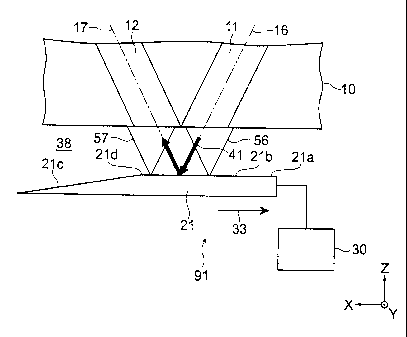
waveguide 11, and again propagates in the optical
2
CA 02487612 2004-11-10
FP03-0353-01
waveguide 11. This light is optical feedback to the
optical waveguide 11. Likewise, light emerging from
the optical waveguide 12 is also scattered by the edge
20b and part thereof returns to the optical waveguide
12. Such optical feedback deforms the waveform of the
signal light propagating in the optical waveguides 11
and 12, so as to cause communication error in certain
cases.
SUMMARY OF THE INVENTION
[0005] It is an object of the present invention to
reduce the optical feedback to at least one of optical
paths in an optical device for changing the power of
light traveling from one optical path to another
optical path.
[0006] Fig. 2 shows a relationship between the
position of the mirror edge 20b and coupling efficiency
in the variable optical attenuator 50 shown in Fig. 1.
When the mirror edge position is 0 pm, the edge 20b is
located on the reference plane 13 between the optical
waveguides 11 and 12. In Fig. 2 a solid line indicates
the coupling efficiency of light traveling from the
optical waveguide 11 to the optical waveguide 12, a
chain line the coupling efficiency of optical feedback
from the optical waveguide 11 to the optical waveguide
11, and a chain double-dashed line the coupling
efficiency of optical feedback from the optical
3
CA 02487612 2004-11-10
FP03-0353-01
waveguide 12 to the optical waveguide 12. In Fig. 2,
the chain line and the chain double-dashed line are
superimposed on each other. In the variable optical
attenuator 50, as shown in Fig. 2, the coupling
efficiencies of optical feedbacks to the optical
waveguides 11 and 12 are high. Therefore, the waveform
of signal light in the optical waveguides is likely to
deform.
[0007] A conceivable method of preventing the
deformation of the waveform of signal light is to
couple isolators 51 and 52 with the optical waveguides
11 and 12, respectively, as shown in Fig. 3. When
signal light 55 propagating through the optical
waveguide 11 is reflected by the movable mirror 20, it
enters the optical waveguide 12 and propagates therein.
Optical feedback 56 to the optical waveguide 11, which
is produced by scattering at the edge 20b of the
movable mirror 20, is blocked by the isolator 51
connected to the optical waveguide 11. The isolator 52
connected to the optical waveguide 12 also blocks
optical feedback 57 from an external device coupled
with the variable optical attenuator 50, to prevent
incidence of the optical feedback 57 into the variable
optical attenuator 50. Therefore, it also prevents
occurrence of optical feedback from the optical
waveguide 12 to the optical waveguide 12. A typical
4
CA 02487612 2004-11-10
FP03-0353-01
tolerance for the coupling efficiency of optical
feedback is -45 dB; however, different tolerances are
determined depending on systems using the variable
optical attenuator.
[0008] The use of isolators as described above can
suppress the influence of optical feedback on the
signal light in an optical communication system using
the . variable optical attenuator. However, the
isolators have to be coupled with the optical
waveguides, which complicates the construction of the
system and which also increases the production cost of
the system. Hence, the Inventors invented new optical
devices capable of reducing the optical feedback.
[0009] In one aspect, the present invention relates
to an optical device. This optical device comprises a
first and second optical path having axes not parallel
to each other, and a light reflecting surface movable
along a predetermined path.
[0010] The light reflecting surface may have a first
planar portion for reflecting light from the first
optical path toward the second optical path, and a
second planar portion having a connection to the first
planar portion. The light reflecting surface may be
movable to allow the connection between the first and
second planar portions to cross the optical axis of the
first optical path. The second planar portion may form
5
CA 02487612 2004-11-10
FP03-0353-01
an angle 01 with the first planar portion. Angle 01
satisfies a condition of 175 <- 01 < 180 in either
clockwise or counterclockwise rotation from the first
planar portion.
[0011] The optical device may further comprise an
optical waveguide for receiving light reflected by the
second planar portion.
[0012] The optical device may further comprise at
least either an optical waveguide optically coupled to
the first optical path or an optical waveguide
optically coupled to the second optical path.
[0013] The light reflecting surface may have a first
planar portion for reflecting light from the first
optical path toward the second optical path, and a
curved portion having a connection to the first planar
portion. The light reflecting surface may be movable
to allow the connection between the first planar
portion and the curved portion to cross the optical
axis of the first optical path. The curved portion may
have a tangent plane at the connection forming an angle
02 with the first planar portion. Angle 02 satisfies a
condition of 175 <- 02 <- 180 in either clockwise or
counterclockwise rotation from the first planar
portion. When 02 is 180. , the curved portion is
smoothly connected to the first planar portion.
6
CA 02487612 2004-11-10
FP03-0353-01
[0014] The light reflecting surface may have a
second planar portion having a connection to the curved
portion at a location away from the first planar
portion. The first planar portion and planes tangent
to the curved portion may form angles that vary
monotonically with their distance from the first planar
portion. The second planar portion may form an angle
03 with a plane tangent to the curved portion at the
location away from the first planar portion. Angle 63
satisfies a condition of 175 _< 63 - 180 in either
clockwise or counterclockwise rotation from the tangent
plane at the location away from the first planar
portion.
[0015] The optical device may further comprise an
optical waveguide for receiving light reflected by the
second planar portion.
[0016] The curved portion may be twisted relative to
the first planar portion.
[0017) The optical device may further comprise at
least either an optical waveguide optically coupled to
the first optical path or an optical waveguide
optically coupled to the second optical path.
[0018] In another aspect, the present invention
relates to an optical device comprising first to Nth (N
is an integer of 2 or more) pairs of optical paths,
each pair including a first and second optical path
7
CA 02487612 2004-11-10
FP03-0353-01
having optical axes not parallel to each other; first
to Nth light reflecting surfaces movable along
predetermined paths; an optical decomposer for
decomposing multiplexed light that contains first to
Nth components having different characteristics into
the first to Nth components; and an optical composer
for combining the decomposed first to Nth components
into the multiplexed light. The Kth (K is an integer
from 1 to N) decomposed component travels through the
first optical path of the Kth pair.
[0019] The Kth reflecting surface may have a first
planar portion for reflecting the Kth decomposed
component from the first optical path of the Kth pair
toward the second optical path of the Kth pair, and a
second planar portion having a connection to the first
planar portion. The Kth reflecting surface may be
movable to allow the connection between the first and
second planar portions of the Kth reflecting surface to
cross the optical axis of the first optical path of the
Kth pair. In the Kth reflecting surface, the second
planar portion may form an angle 61 with the first
planar portion. Angle 81 satisfies a condition of 175
< Ai < 180 in either clockwise or counterclockwise
rotation from the first planar portion. The optical
composer combines the first to Nth components traveling
on the second optical paths of the first to Nth pairs.
8
CA 02487612 2004-11-10
FP03-0353-01
[0020] The Kth reflecting surface may have a first
planar portion for reflecting the Kth decomposed
component from the first optical path of the Kth pair
toward the second optical path of the Kth pair, and a
curved portion having a connection to the first planar
portion. The Kth reflecting surface may be movable to
allow the connection between the first planar portion
and the curved portion of the Kth reflecting surface to
cross the optical axis of the first optical path of the
Kth pair. In the Kth reflecting surface, the curved
portion may have a tangent plane at the connection
forming an angle 82 with the first planar portion.
Angle 82 satisfies a condition of 175 < 82 < 180 in
either clockwise or counterclockwise rotation from the
first planar portion. The optical composer may combine
the first to Nth components traveling on the second
optical paths of the first to Nth pairs.
[0021] The first to Nth components may have
different wavelengths. The multiplexed light may be
wavelength-multiplexed light that contains the first to
Nth components. The optical decomposer may be an
optical demultiplexer for demultiplexing the
wavelength-multiplexed light into the first to Nth
components. The optical composer may be an optical
multiplexer for multiplexing the first to Nth
components into the wavelength-multiplexed light.
9
CA 02487612 2004-11-10
FP03-0353-01
[0022] In further aspect, the present invention
relates to a movable reflector comprising a light
reflecting surface, and a driver device capable of
moving the light reflecting surface along a
predetermined movement path.
[0023] The light reflecting surface may have a first
planar portion, and a second planar portion having a
connection to the first planar portion. The second
planar portion may form an angle 01 with the first
planar portion. Angle 01 satisfies a condition of 175
-< 01 < 180 in either clockwise or counterclockwise
rotation from the first planar portion.
[0024] The light reflecting surface may have a first
planar portion, and a curved portion having a
connection to the first planar portion. The curved
portion may have a tangent plane at the connection
forming an angle 02 with the first planar portion.
Angle 02 satisfies a condition of 175 <- 02 -< 180 in
either clockwise or counterclockwise rotation from the
first planar portion. When 02 is 180 , the curved
portion is smoothly connected to the first planar
portion.
[0025] The light reflecting surface may have a
second planar portion having a connection to the curved
portion at a location away from the first planar
portion. The first planar portion and planes tangent
CA 02487612 2011-03-25
to the curved portion may form angles that vary
monotonically with their distance from the first planar
portion. The second planar portion may form an angle
03 with a plane tangent to the curved portion at the
location away from the first planar portion. Angle 03
satisfies a condition of 175 _< 03 < 180 in either
clockwise or counterclockwise rotation from the tangent
plane at the location away from the first planar
portion.
[0026] The curved portion may be twisted relative to
the first planar portion.
[0027] Further scope of applicability of the present
invention will become apparent from the detailed
description given hereinafter. However, it should be
understood that the detailed description and specific
examples, while indicating preferred embodiments of the
invention, are given by way of illustration only, since
various changes and modifications within the spirit and
scope of the invention will become apparent to those
skilled in the art from this detailed description.
In one aspect, the invention provides an optical
device, comprising:
a first and second optical path having axes not
parallel to each other; and
a light reflecting surface movable along a
predetermined path;
the light reflecting surface having a first planar
portion for reflecting light from the first optical path
11
CA 02487612 2011-03-25
toward the second optical path, and a curved portion
having a connection to the first planar portion;
the light reflecting surface being movable to allow
the connection between the first planar portion and the
curved portion to cross the optical axis of the first
optical path; and
the curved portion having a tangent plane at the
connection forming an angle 02 with the first planar
portion, angle 02 satisfying a condition of 175 < 02 <
180 in a clockwise or in a counterclockwise rotation
from the first planar portion;
wherein the light reflecting surface has a second
planar portion having a connection to the curved portion
at a location away from the first planar portion;
wherein the first planar portion and planes tangent
to the curved portion form angles that vary
monotonically with their distance from the first planar
portion; and
wherein the second planar portion forms an angle 03
with a plane tangent to the curved portion at the
location away from the first planar portion, angle 03
satisfying a condition of 175 < 03 < 180 in a
clockwise or in a counterclockwise rotation from the
tangent plane at the location away from the first planar
portion.
In one aspect, the invention provides an optical
device, comprising:
lla
CA 02487612 2011-03-25
a first and second optical path having axes not
parallel to each other; and
a light reflecting surface movable along a
predetermined path;
the light reflecting surface having a first planar
portion for reflecting light from the first optical path
toward the second optical path, and a curved portion
having a connection to the first planar portion;
the light reflecting surface being movable to allow
the connection between the first planar portion and the
curved portion to cross the optical axis of the first
optical path; and
the curved portion having a tangent plane at the
connection forming an angle 02 with the first planar
portion, angle 02 satisfying a condition of 175 < 02 <
1800 in a clockwise or in a counterclockwise rotation
from the first planar portion;
wherein the curved portion is twisted relative to
the first planar portion.
In one aspect, the invention provides a movable
reflector comprising:
a light reflecting surface; and
a driver device capable of moving the light
reflecting surface along a predetermined movement path,
the light reflecting surface having a first planar
portion, and a curved portion having a connection to the
first planar portion,
llb
CA 02487612 2011-03-25
the curved portion having a tangent plane at the
connection forming an angle 02 with the first planar
portion, angle 02 satisfying a condition of 175 < 02 <
180 in a clockwise or in a counterclockwise rotation
from the first planar portion,
wherein the light reflecting surface has a second
planar portion having a connection to the curved portion
at a location away from the first planar portion;
wherein the first planar portion and planes tangent
to the curved portion form angles that vary
monotonically with their distance from the first planar
portion; and
wherein the second planar portion forms an angle 03
with a plane tangent to the curved portion at the
location away from the first planar portion, angle 83
satisfying a condition of 175 < 03 < 180 in a
clockwise or in a counterclockwise rotation from the
tangent plane at the location away from the first planar
portion.
In one aspect, the invention provides a movable
reflector comprising:
a light reflecting surface; and
a driver device capable of moving the light
reflecting surface along a predetermined movement path,
the light reflecting surface having a first planar
portion, and a curved portion having a connection to the
first planar portion,
llc
CA 02487612 2011-03-25
the curved portion having a tangent plane at the
connection forming an angle 02 with the first planar
portion, angle 02 satisfying a condition of 175 < 02 <
180 in a clockwise or in a counterclockwise rotation
from the first planar portion,
wherein the curved portion is twisted relative to
the first planar portion.
BRIEF DESCRIPTION OF THE DRAWINGS
[0028] Fig. 1 is a schematic plan view showing an
example of a variable optical attenuator.
[0029] Fig. 2 is a diagram showing a relationship
between the location of an edge of a movable mirror and
the coupling efficiency.
lid
CA 02487612 2004-11-10
FP03-0353-01
[0030] Fig. 3 is a schematic diagram showing a
method of reducing optical feedback.
[0031] Fig. 4 is a schematic plan view showing a
variable optical attenuator of a first embodiment.
[0032] Fig. 5 is a schematic plan view showing
reflection of light by a first planar portion of a
movable mirror.
[0033] Fig. 6 is a schematic plan view showing
reflection of light by a second planar portion of a
movable mirror.
[0034] Fig. 7 is a diagram showing a relationship
between an angle of a second planar portion and the
coupling efficiency of optical feedback.
[0035] Fig. 8 is a schematic plan view showing a
variable optical attenuator of a second embodiment.
[0036] Fig. 9 is a schematic plan view showing a
variable optical attenuator of a third embodiment.
[0037] Fig. 10 is a schematic plan view showing a
variable optical attenuator of a fourth embodiment.
[0038] Fig. 11 is a schematic plan view showing
reflection of light by a curved portion of a movable
mirror.
[0039] Fig. 12 is a diagram showing a relationship
between the amount of the movement of a movable mirror
and the coupling efficiency.
12
CA 02487612 2004-11-10
FP03-0353-01
[0040] Fig. 13 is a diagram showing a relationship
between the curvature of a curved portion and the
coupling efficiency of optical feedback.
[0041] Fig. 14 is a table showing typical values on
the graph shown in Fig. 13.
[0042] Fig. 15 is a diagram showing a relationship
between the amount of the movement of a movable mirror
and the coupling efficiency.
[0043] Fig. 16 is a diagram showing a relationship
between the movement of the amount of a movable mirror
and the coupling efficiency.
[0044] Fig. 17 is a schematic plan view showing
reflection of light by a curved portion of a movable
mirror.
[0045] Fig. 18 is a schematic plan view showing a
variable optical attenuator in the fifth embodiment.
[0046] Fig. 19 is a diagram showing a relationship
between the amount of the movement of a movable mirror
and the coupling efficiency.
[0047] Fig. 20 is a schematic plan view showing a
variable optical attenuator of a sixth embodiment.
[0048] Fig. 21 is a schematic plan view showing a
variable optical attenuator of a seventh embodiment.
[0049] Fig. 22 is a schematic perspective view
showing a movable mirror in the seventh embodiment.
13
CA 02487612 2004-11-10
FP03-0353-01
[0050] Fig. 23 is a diagram showing a relationship
between the amount of the movement of a movable mirror
and the coupling efficiency.
[0051] Fig. 24 is a schematic plan view showing a
variable optical attenuator of an eighth embodiment.
[0052] Fig. 25 is a schematic side view showing the
variable optical attenuator in the eighth embodiment.
[0053] Fig. 26 is a schematic plan view showing
other examples of the movable mirrors.
[0054] Fig. 27 is a schematic plan view showing
other examples of the optical waveguides.
DESCRIPTION OF THE PREFERRED EMBODIMENTS
[0055] The preferred embodiments of the present
invention will be described below in greater detail
with reference to the accompanying drawings. To
facilitate understanding, identical reference numerals
are used, where possible, to designate identical or
equivalent elements that are common to the embodiments,
and, in subsequent embodiments, these elements will not
be further explained.
[0056] First Embodiment
Fig. 4 is a schematic plan view showing an optical
device of the first embodiment. This optical device is
a variable optical attenuator 100. The variable
optical attenuator 100 has a Planar Lightwave Circuit
(PLC) 10, a movable mirror 21, and a mirror driver
14
CA 02487612 2004-11-10
FP03-0353-01
device 30. The mirror 21 and the mirror driver device
30 constitute a movable reflector 91. These components
are set in a housing (not shown).
[0057] PLC 10 has two optical waveguides 11 and 12.
The optical waveguides 11 and 12 are planar waveguides
extending in parallel with the plane of Fig. 4. The
optical waveguides 11 and 12 are made, for example, of
silica glass. The optical waveguides 11 and 12, as
shown in Fig. 4, have their respective end portions
arranged in symmetry (in mirror symmetry in the present
embodiment) with respect to a reference plane 13
perpendicular to the plane of Fig. 4. Each of these
end portions linearly extends with an inclination of an
angle a relative to the reference plane 13. At these
end portions, an angle 2a is formed between an optical
axis 16 of the optical waveguide 11 and an optical axis
17 of the optical waveguide 12. An end face 11a of the
optical waveguide 11 and an end face 12a of the optical
waveguide 12 are placed on a plane normal to the plane
of Fig. 4.
[0058] The movable mirror 21 is an optical reflector
having a light reflecting surface 21a. The movable
mirror 21 is a prism extending perpendicularly to the
plane of Fig. 4, and has a uniform cross section along
the direction normal to the plane of Fig. 4. The light
reflecting surface 21a has an extremely high
CA 02487612 2004-11-10
FP03-0353-01
reflectance (e.g., 90% or more) for light of a
predetermined wavelength propagating in the optical
waveguides 11 and 12. The light reflecting surface 21a
faces the end faces lla and 12a of the optical
waveguides 11 and 12. The clearance between the light
reflecting surface 21a and the end faces lla and 12a
may be filled with an index matching material 38.
[0059] The light reflecting surface 21a includes a
first planar portion 21b and a second planar portion
21c connected to each other. The connection (boundary)
between the first planar portion 21b and the second
planar portion 21c forms an edge 21d. The first and
second planar portions 21b and 21c, and the edge 21d
all extend perpendicularly to the plane of Fig. 4. The
first planar portion 21b is parallel to the end faces
11a and 12a of the optical waveguides 11 and 12. As
shown in Fig. 4, the second planar portion 21c forms an
angle of 01 in clockwise rotation from the first planar
portion 21b. The angle 01 is a supplement of an acute
angle 00 between the first planar portion 21b and an
extending plane from the second planar portion 21c.
That is, 80 + 01 = 180 . In the present embodiment, as
described later, 175 <- 01 < 180 , and 0 < 00 < 5 .
[0060] An XYZ orthogonal coordinate system is
depicted in Fig. 4, for convenience' sake of
description. The X-axis extends along a line of
16
CA 02487612 2004-11-10
FP03-0353-01
intersection between the first planar portion 21b and a
plane including both the optical axes 16 and 17 of the
waveguides 11 and 12. The Y-axis extends
perpendicularly to the X-axis in the plane normal to a
bisector of the angle between the optical axes 16 and
17. The Z-axis extends in parallel with the bisector.
[0061] The mirror driver device 30 moves the movable
mirror 21 in directions nearly parallel to the end
faces 11a and 12a of the optical waveguides 11 and 12,
as indicated by arrows 32 and 33. In other words, the
mirror driver device 30 moves the movable mirror 21
substantially in parallel with the XY plane. In
accordance therewith, the light reflecting surface 21a
of the movable mirror 21 moves along a movement path 76
substantially parallel to the XY plane. The movement
of the movable mirror 21 is reversible. Light from the
optical waveguides 11 and 12 is reflected by the first
planar portion 21b or by the second planar portion 21c,
depending upon the location of the light reflecting
surface 21a. An example of the mirror driver device 30
is an electrostatic actuator as described in C. Marxer
et al. mentioned above.
[0062] In the present embodiment, the movement path
76 is of linear shape extending substantially in the X-
direction. However, the movement path 76 may also be
of curved shape. If curvature is sufficiently large,
17
CA 02487/612 2004-11-10
FP03-0353-01
the light reflecting surface 21a can be moved
substantially in the X-direction in the vicinity of the
end faces of the optical waveguides 11 and 12.
[0063] Fig. 5 shows reflection of light 41 emerging
from the optical waveguide 11 along its optical axis 16
by the first planar portion 21b. As shown in Fig. 5,
the variable optical attenuator 100 has optical paths
56 and 57 not parallel to each other. The optical
paths 56 and 57 are formed by the optical waveguides 11
and 12. The optical paths 56 and 57 extend between the
end faces 11a and 12a of the optical waveguides 11 and
12 and the light reflecting surface 21a, and are
optically coupled to the respective optical waveguides
11 and 12. In the present embodiment the clearance
between the end faces of the optical waveguides 11 and
12 and the light reflecting surface 21a is filled with
the index matching material 38 having a refractive
index nearly equal to that of the optical waveguides 11
and 12. For this reason, the optical axes of the
optical paths 56 and 57 substantially agree with the
optical axes 16 and 17 of the optical waveguides 11 and
12, respectively. The light reflecting surface 21a
moves so as to intersect with the optical paths 56 and
57. The connection between the first planar portion
21b and the second planar portion 21c is movable across
18
CA 02487612 2004-11-10
FP03-0353-01
the optical axes 16 and 17 of these optical paths 56
and 57.
[0064] When the movable mirror 21 is placed at the
location as shown in Fig. 5, the light 41 emerging from
the optical waveguide 11 travels on the optical path 56
toward the mirror 21 and then impinges on the first
planar portion 21b. When the first planar portion 21b
receives the light 41 from the optical path 56, it
reflects the light 41 into the optical path 57 along
the optical axis 17. In consequence, the light 41 from
the optical waveguide 11 travels along the optical axis
17 into the optical waveguide 12 and propagates in the
optical waveguide 12.
[0065] As the movable mirror 21 moves in the
direction indicated by the arrow 33 from the location
shown in Fig. 5, the light 41 comes to be reflected by
the second planar portion 21c, as shown in Fig. 6.
When the second planar portion 21c receives the light
41, it reflects the light 41 into a direction deviated
from the optical axis 17. This decreases the coupling
efficiency from the optical path 56 to the optical path
57, and correspondingly the coupling efficiency from
the optical waveguide 11 to the optical waveguide 12.
[0066] During the movement from the location shown
in Fig. 5 to the location shown in Fig. 6, the vicinity
of the edge 21d of the movable mirror 21 is irradiated
19
CA 02487612 2004-11-10
FP03-0353-01
with the light from the optical waveguide 11. In
general, light transmitted by an optical waveguide has
some divergence in a plane normal to the optical axis
of the optical waveguide and the size of the divergence
is represented by a Mode Field Diameter (MFD). Hence,
when the light from the optical waveguide 11 reaches
the vicinity of the edge 21d, part of the light is
reflected by the first planar portion 21b and the rest
is reflected by the second planar portion 21c. The
component reflected by the second planar portion 21c is
unlikely to be coupled with the optical path 57 and
with the optical waveguide 12. The quantities of light
received by the first and second planar portions 21b
and 21c vary according to the movement of the light
reflecting surface 21a. Therefore, the power of the
light propagating from the optical path 56 to the
optical path 57 and the power of the light propagating
from the optical waveguide 11 to the optical waveguide
12 can be continuously changed according to the
movement of the light reflecting surface 21a.
Likewise, the power of the light propagating from the
optical path 57 to the optical path 56 and the power of
the light propagating from the optical waveguide 12 to
the optical waveguide 11 can also be changed according
to the movement of the light reflecting surface 21a.
CA 021487612 2004-11-10
FP03-0353-01
[0067] In the present embodiment, the angle el of
the edge 21d of the movable mirror 21 is large enough
to reduce the light emerging from the optical waveguide
11 and then returning to the optical waveguide 11.
This means reduction of the light coming from the
optical path 56 onto the movable mirror 21 and then
returning to the optical path 56. Fig. 7 shows a
relationship between the angle 80 shown in Fig. 4 and
the coupling efficiency of the optical feedback to the
optical waveguide 11. It is assumed herein that the
light transmitted by the optical waveguides 11 and 12
has the wavelength of 1.55 pm and the Gaussian
distribution with the Mode Field Diameter (MFD) of 20
pm, that the angle 2a between the optical waveguides 11
and 12 is 10 , and that the clearance between the end
faces lla and 12a of the optical waveguides 11 and 12
and the light reflecting surface 21a is filled with the
index matching material 38 having the refractive index
of 1.45. As shown in Fig. 7, in the range where the
angle e0 is not more than 5 , the coupling efficiency
of the optical feedback drastically drops.
[0068] In the present embodiment the angle el of the
edge 21d is in the range of 175 <_ el < 180 , so that
the angle 80 satisfies the condition of 0 < e0 <_ 5 .
Therefore, the optical feedback from the optical
waveguide 11 to the optical waveguide 11 can be
21
CA 02487612 2004-11-10
FP03-0353-01
adequately reduced. For this reason, the variable
optical attenuator 100 suitably operates even if the
isolator for blocking the optical feedback is not
connected to the optical waveguide 11. As a result, it
is feasible to readily and inexpensively construct an
optical system incorporating the variable optical
attenuator 100.
[00691 Second Embodiment
Fig. 8 is a schematic plan view showing a variable
optical attenuator 200 in the second embodiment. The
variable optical attenuator 200 has a PLC 60 instead of
the PLC 10 in the variable optical attenuator 100 in
the first embodiment. The other structure of the
variable optical attenuator 200 is the same as in the
first embodiment.
[00701 The PLC 60 has three optical waveguides 61,
62, and 63. These optical waveguides are planar
waveguides extending in parallel with the plane of Fig.
8, and are made, for example, of silica glass. The
optical waveguides 61 and 62 have their respective ends
placed in symmetry (in mirror symmetry in the present
embodiment) with respect to a reference plane including
the optical axis 68 of the optical waveguide 63 and
perpendicular to the plane of Fig. 8. These ends each
linearly extend with an inclination of an angle a
relative to the optical axis 68. Therefore, these ends
22
CA 02487612 2004-11-10
FP03-0353-01
form an angle 2a. End faces 61a - 63a of the optical
waveguides 61 - 63 all are placed on a plane normal to
the plane of Fig. 8.
[0071] The variable optical attenuator 200 has
optical paths 56 - 58 each extending between the end
faces of the optical waveguides 61 - 63 and the light
reflecting surface 21a. In the present embodiment the
clearance between the end faces of the optical
waveguides 61 - 63 and the light reflecting surface 21a
is filled with the index matching material 38 having
the refractive index approximately equal to that of the
optical waveguides 61 - 63. For this reason, the
optical axes of the respective optical paths 56 - 58
substantially agree with the optical axes 66 - 68 of
the optical waveguides 61 - 63, respectively.
[0072] As shown in Fig. 8, the optical path 58 and
the optical waveguide 63 are arranged so that when the
light 44 emerging along the optical axis 67 from the
optical waveguide 62 is reflected by the second planar
portion 21c, they receive the light 44 along the
optical axis 68. Therefore, the light 44 reflected by
the second planar portion 21c travels on the optical
path 58 to enter the optical waveguide 63, and
propagates in the optical waveguide 63. This can
prevent the light from the optical waveguide 62
reflected by the second planar portion 21c from being
23
CA 02487612 2004-11-10
FP03-0353-01
coupled with another optical device in an optical
system incorporating the variable optical attenuator
200.
[0073] As shown in Fig. 8, when the signal light 46
from the optical waveguide 61 is reflected by the
second planar portion 21c, it travels off the optical
path 57 to the side of the optical waveguide 62. If
another optical waveguide exists beside the optical
waveguide 62, the signal light 46 may be coupled with
the optical waveguide. Where the signal light
propagates in the optical waveguide, this optical
coupling can cause crosstalk. In order to prevent the
crosstalk, it is preferable to transmit the signal
light from the optical waveguide 62 to the optical
waveguide 61. In this case, light emerging from the
end face 61a of the optical waveguide 61 is light at
low intensity mainly reflected by an external optical
device. Consequently, the crosstalk can be
satisfactorily suppressed. This also applies to the
variable optical attenuator of the first embodiment.
[0074] Third Embodiment
Fig. 9 is a schematic plan view showing a variable
optical attenuator 300 in the third embodiment. The
variable optical attenuator 300 has a movable mirror 22
instead of the movable mirror 21 in the variable
optical attenuator 100 of the first embodiment. The
24
CA 02487612 2004-11-10
FP03-0353-01
mirror 22 and mirror driver device 30 constitute a
movable reflector 92. The other structure of the
variable optical attenuator 300 is the same as in the
first embodiment.
[0075] The movable mirror 22 is an optical reflector
having a light reflecting surface 22a. The movable
mirror 22 is a prism extending perpendicularly to the
plane of Fig. 9, and has a uniform cross section along
the direction normal to the plane of Fig. 9. The light
reflecting surface 22a has an extremely high
reflectance (e.g., 90% or more) for light of a
predetermined wavelength propagating in the optical
waveguides 11 and 12. The light reflecting surface 22a
faces the end faces lla and 12a of the optical
waveguides 11 and 12. The clearance between the light
reflecting surface 22a and the end faces lla and 12a
may be filled with the index matching material 38.
[0076] Unlike the light reflecting surface 21a in
the first embodiment, the light reflecting surface 22a
includes a planar portion 22b and a curved portion 22c
connected to each other. The connection (boundary)
between the planar portion 22b and the curved portion
22c forms an edge 22d. The planar portion 22b, curved
portion 22c, and edge 22d all extend perpendicularly to
the plane of Fig. 9. The planar portion 22b is
parallel to the end faces lla and 12a of the optical
CA 02487612 2004-11-10
FP03-0353-01
waveguides 11 and 12. The planar portion 22b and
planes tangent to the curved portion 22c form angles
that monotonically vary with their distance from the
planar portion 22b. The tangent plane of the curved
portion 22c at the edge 22d forms an angle of 02 in
clockwise rotation from the planar portion 22b. In the
present embodiment, 175 <- 02 < 1800.
[0077] The mirror driver device 30 moves the movable
mirror 22 in directions nearly parallel to the end
faces lla and 12a of the optical waveguides 11 and 12,
as indicated by arrows 32 and 33. In accordance
therewith, the light reflecting surface 22a of the
movable mirror 22 moves along a movement path 76. The
connection between the planar portion 22b and the
curved portion 22c is movable across the optical axes
16 and 17 of the optical paths 56 and 57. Light
emerging from the optical waveguides 11 and 12 is
reflected by the planar portion 22b or by the curved
portion 22c in accordance with the location of the
light reflecting surface 22a.
[0078] Just as the planar portion 21b in the first
embodiment does, the planar portion 22b receives the
light 41 emerging along the optical axis 16 from the
optical waveguide 11 and propagating on the optical
path 56 and then reflects the light 41 along the
optical axis 17 to the optical path 57. In
26
CA 02487612 2004-11-10
FP03-0353-01
consequence, the light 41 from the optical waveguide 11
is incident along the optical axis 17 into the optical
waveguide 12. Therefore, when the light from the
optical waveguide 11 is reflected by the planar portion
22b, the coupling efficiency from the optical path 56
to the optical path 57 and the coupling efficiency from
the optical waveguide 11 to the optical waveguide 12
are high. On the other hand, when the curved portion
22c receives the light 41, it reflects the light 41
into directions deviated from the optical axis 17.
This decreases the coupling efficiency from the optical
path 56 to the optical path 57 and the coupling
efficiency from the optical waveguide 11 to the optical
waveguide 12. Therefore, as in the first embodiment,
the variable optical. attenuator 300 can continuously
change the power of light propagating in the path from
the optical waveguide 11 to the optical waveguide 12,
or in the reverse path, according to the movement of
the light reflecting surface 22a.
[0079] Just as in the first embodiment, in the
present embodiment the angle 92 of the edge 22d of the
movable mirror 22 is large enough to reduce the light
emerging from the optical waveguide 11 and then
returning to the optical waveguide 11. For this
reason, the variable optical attenuator 300 suitably
operates even if the isolator for blocking the optical
27
CA 02487612 2004-11-10
FP03-0353-01
feedback is not connected to the optical waveguide 11.
Therefore, it is feasible to readily and inexpensively
construct an optical system incorporating the variable
optical attenuator 300.
[0080] Fourth Embodiment
Fig. 10 is a schematic plan view showing a
variable optical attenuator 400 in the fourth
embodiment. The variable optical attenuator 400 has a
movable mirror 23 instead of the movable mirror 22 in
the variable optical attenuator 300 of the third
embodiment. The mirror 23 and mirror driver device 30
constitute a movable reflector 93. The other structure
of the variable optical attenuator 400 is the same as
in the third embodiment.
[0081] The movable mirror 23 is an optical reflector
having a light reflecting surface 23a. The movable
mirror 23 is a prism extending perpendicularly to the
plane of Fig. 10, and has a uniform cross section along
the direction normal to the plane of Fig. 10. The
light reflecting surface 23a has an extremely high
reflectance (e.g., 90% or more) for light of the
predetermined wavelength propagating in the optical
waveguides 11 and 12. The light reflecting surface 23a
faces the end faces 11a and 12a of the optical
waveguides 11 and 12. The clearance between the light
28
CA 02487612 2004-11-10
FP03-0353-01
reflecting surface 23a and the end faces Ila and 12a
may be filled with the index matching material 38.
[0082] As the light reflecting surface 22a in the
third embodiment was, the light reflecting surface 23a
includes a planar portion 23b and a curved portion 23c
connected to each other. However, different from the
third embodiment, the connection (boundary) between the
planar portion 23b and the curved portion 23c forms no
edge. In other words, a tangent plane at an end, which
is connected to the planar portion 23b, of the curved
portion 23c forms an angle of 180 in clockwise
rotation from the planar portion 23b. Hence, the
planar portion 23b and the curved portion 23c are
smoothly connected on a boundary plane 70 perpendicular
to the plane of Fig. 10. Both the planar portion 23b
and the curved portion 23c extend perpendicularly to
the plane of Fig. 10. The planar portion 23b is
parallel to the end faces Ila and 12a of the optical
waveguides 11 and 12. The planar portion 23b and
planes tangent to the curved portion 23c form angles
that vary monotonically with their distance from the
planar portion 23b.
[0083] The mirror driver device 30 moves the movable
mirror 23 in directions nearly parallel to the end
faces Ila and 12a of the optical waveguides 11 and 12,
as indicated by arrows 32 and 33. In accordance
29
CA 02487612 2004-11-10
FP03-0353-01
therewith, the light reflecting surface 23a of the
movable mirror 23 moves along the movement path 76.
The connection between the planar portion 23b and the
curved portion 23c is movable across the optical axes
16 and 17 of the optical paths 56 and 57. The light
emerging from the optical waveguides 11 and 12 is
reflected by the planar portion 23b or by the curved
portion 23c in accordance with the location of the
light reflecting surface 23a.
[0084] Fig. 10 shows reflection of the light 41
emerging from the optical waveguide 11 along the
optical axis 16 by the planar portion 23b. When the
movable mirror 23 is placed at the location shown in
Fig. 10, the light 41 emerging from the optical
waveguide 11 travels on the optical path 56 toward the
mirror 23 and then impinges on the planar portion 23b.
When the planar portion 23b receives the light 41 from
the optical path 56, it reflects the light 41 toward
the optical path 57 along the optical axis 17. In
consequence, the light 41 from the optical waveguide 11
is incident along the optical axis 17 into the optical
waveguide 12. Therefore, when the light from the
optical waveguide 11 is reflected by the planar portion
23b, the coupling efficiency from the optical waveguide
11 to the optical waveguide 12 is high. As the movable
mirror 23 moves in the direction indicated by the arrow
CA 02487612 2004-11-10
FP03-0353-01
33, as shown in Fig. 11, the light 41 comes to be
reflected by the curved portion 23c. The curved
portion 23c reflects the light 41 into directions
deviated from the optical axis 17. This decreases the
coupling efficiency from the optical path 56 to the
optical path 57, and correspondingly the coupling
efficiency from the optical waveguide 11 to the optical
waveguide 12. Therefore, as in the first embodiment,
the variable optical attenuator 400 can continuously
change the power of light propagating in the path from
the optical waveguide 11 to the optical waveguide 12,
or in the reverse path, according to the movement of
the light reflecting surface 23a.
[0085] An example in which the curved portion 23c is
a cylindrical surface will be described below. In this
example, the light transmitted by the optical
waveguides 11 and 12 has the wavelength of 1.55 pm, and
the Gaussian distribution with the Mode Field Diameter
(MFD) of 20 pm. The radius of curvature of the curved
portion 23c is 400 pm, and the angle 2a between the
optical waveguides 11 and 12 is 100. The clearance
between the end faces lla and 12a of the optical
waveguides 11 and 12 and the light reflecting surface
23a is filled with the index matching material 38
having the refractive index of 1.45.
31
CA 02487612 2004-11-10
FP03-0353-01
[0086] Fig. 12 shows a relationship between the
movement amount of the movable mirror 23 and the
coupling efficiency between the optical waveguides 11
and 12. The "MIRROR MOVEMENT" on the horizontal axis
represents the amount of movement of the movable mirror
23 along the direction indicated by the arrow 33 in
Fig. 11. When the mirror movement amount is 25 pm, the
boundary plane 70 between the planar portion 23b and
the curved portion 23c coincides with the reference
plane 13 located midway between the optical waveguides
11 and 12. When the mirror movement amount is less
than 25 pm, as shown in Fig. 10, the light from the
optical waveguide 11 is reflected mainly by the planar
portion 23b. When the mirror movement amount is over
25 pm, as shown in Fig. 11, the light from the optical
waveguide 11 is reflected mainly by the curved portion
23c.
[0087] In Fig. 12 a solid line indicates the
coupling efficiency of the light traveling from the
optical waveguide 11 to the optical waveguide 12, a
chain line the coupling efficiency of the light
emerging from the optical waveguide 11 and returning to
the optical waveguide 11, and a chain double-dashed
line the coupling efficiency of the light emerging from
the optical waveguide 12 and returning to the optical
waveguide 12. As shown in Fig. 12, the coupling
32
CA 02487612 2004-11-10
FP03-0353-01
efficiency from the optical waveguide 11 to the optical
waveguide 12 monotonically decreases as the mirror
movement amount increases from about 25 pm. The
coupling efficiency of the optical feedback from the
optical waveguide 11 to the optical waveguide 11 is at
most about -50 dB. In contrast to it, in the case of
the variable optical attenuator 50 using the movable
mirror 20 without the curved portion, as shown in Fig.
2, the coupling efficiency of the optical feedback to
the optical waveguide 11 exceeds -25 dB.
[0088] As described above, the variable optical
attenuator 400 of the present embodiment is able to
significantly reduce the optical feedback to the
optical path 56 and to the optical waveguide 11. This
is conceivably because the planar portion 23b and the
curved portion 23c are smoothly connected with no edge
between them. Since the optical feedback to the
optical waveguide 11 is sufficiently small, the
variable optical attenuator 400 suitably operates even
if the isolator for blocking the optical feedback is
not connected to the optical waveguide 11. Therefore,
it is feasible to readily and inexpensively construct
an optical system incorporating the variable optical
attenuator 400.
[0089] The preferred curvature of the curved portion
23c will be discussed below where the curved portion
33
CA 02487612 2004-11-10
FP03-0353-01
23c is a cylindrical surface. Fig. 13 is a graph
showing a relationship between the curvature of the
curved portion 23c of the cylindrical surface and the
coupling efficiency of the optical feedback from the
optical waveguide 11 to the optical waveguide 11. Fig.
14 is a table showing typical values on the graph of
Fig. 13, where "OFB" represents the quantity of the
optical feedback, "CUR" the curvature of the curved
portion, and "ROC" the radius of curvature of the
curved portion. Here the wavelength, the MFD, the
angle between the waveguides 11 and 12, and the
refractive index of the index matching material are the
same as in the case of Fig. 12, and are 1.55 pm, 20 pm,
10 , and 1.45, respectively. As shown in Fig. 13, the
coupling efficiency of the optical feedback drastically
drops in the region where the curvature of the curved
portion 23c is not more than 0.02/pm. Therefore, the
radius of curvature of the curved portion 23c is
preferably not less than the reciprocal of the
curvature of 0.02/pm, i.e., not less than 50 pm.
[0090] The relationship between the radius of
curvature of the curved portion 23c and the coupling
efficiency of the optical feedback varies according to
the wavelength, the MFD, the angle between optical
waveguides, and the refractive index of the clearance
between the optical waveguides and the movable mirror.
34
CA 02487612 2004-11-10
FP03-0353-01
The minimum curvature radius to achieve sufficient
feedback reducing effect is inversely proportional to
the wavelength, is proportional to the square of the
MFD, and is proportional to the refractive index of the
clearance between the optical waveguides and the
movable mirror. For example, where the MFD is half of
that in the above example, i.e., 10 pm, the minimum
curvature radius for reduction of optical feedback is a
quarter of 50 pm, i.e., 12.5 pm. In this case, the
radius of curvature of the curved portion 23c is
preferably 12.5 pm or more.
[0091] The curved portion 23c does not always have
to be a cylindrical surface. Fig. 15 shows a
relationship between the mirror movement amount and the
coupling efficiency where the shape of the curved
portion 23c is expressed by a cubic function of y =
0.0003 x x3. Fig. 16 shows a relationship between the
mirror movement amount and the coupling efficiency
where the shape of the curved portion 23c is expressed
by a sextic function of y = 10-7 x X6 Here the origin
of the xy coordinates is located at the boundary
between the curved portion 23c and the planar portion
23b, the x-axis is parallel to the planar portion 23b,
and the y-axis is normal to the planar portion 23b.
Units of x and y are pm. The other conditions are the
same as in the above example.
CA 02487612 2004-11-10
FP03-0353-01
[0092] In Figs. 15 and 16 a solid line indicates the
coupling efficiency of the light traveling from the
optical waveguide 11 to the optical waveguide 12, a
chain line the coupling efficiency of the light
emerging from the optical waveguide 11 and returning to
the optical waveguide 11, and a chain double-dashed
line the coupling efficiency of the light emerging from
the optical waveguide 12 and returning to the optical
waveguide 12. As seen from these figures, the optical
feedback to the optical waveguide 11 is fully reduced
even in cases where the curved portion 23c is not a
cylindrical surface.
[0093] If the radius of curvature of the curved
portion 23c is too small, the optical feedback due to
diffraction will increase. An appropriate radius of
curvature is determined according to the wavelength and
divergence of light, the angle between waveguides, and
so on.
[0094] Fifth Embodiment
In the foregoing embodiments the optical feedback
from the optical waveguide 11 to the optical waveguide
11 is reduced well, but the reduction of the optical
feedback from the optical waveguide 12 to the optical
waveguide 12 is not enough. As shown in Fig. 17, when
the light 43 emerging along the optical axis 17 from
the optical waveguide 12 and propagating on the optical
36
CA 02487612 2004-11-10
FP03-0353-01
path 57 is reflected by the curved portion 23c, it is
likely to return to the optical path 57 and to the
optical waveguide 12. Therefore, the fifth embodiment
of the present invention presents a variable optical
attenuator 500 capable of also reducing the optical
feedback to the optical path 57 and to the optical
waveguide 12 as well as the optical feedback to the
optical path 56 and to the optical waveguide 11.
[0095] Fig. 18 is a schematic plan view showing the
variable optical attenuator 500 in the fifth
embodiment. The variable optical attenuator 500 has a
movable mirror 24 instead of the movable mirror 23 in
the variable optical attenuator 400 in the fourth
embodiment. The mirror 24 and mirror driver device 30
constitute a movable reflector 94. The other structure
of the variable optical attenuator 500 is much the same
as in the fourth embodiment.
[0096] The movable mirror 24 is an optical reflector
having a light reflecting surface 24a. The movable
mirror 24 is a prism extending perpendicularly to the
plane of Fig. 18, and has a uniform cross section along
the direction normal to the plane of Fig. 18. The
light reflecting surface 24a has an extremely high
reflectance (e.g., 90% or more) for light of the
predetermined wavelength propagating in the optical
waveguides 11 and 12. The light reflecting surface 24a
37
CA 02487612 2004-11-10
FP03-0353-01
faces the end faces lla and 12a of the optical
waveguides 11 and 12. The clearance between the light
reflecting surface 24a and the end faces lla and 12a
may be filled with the index matching material 38.
[0097] The light reflecting surface 24a has a second
planar portion 24d in addition to the first planar
portion 24b and the curved portion 24c. The first
planar portion 24b, curved portion 24c, and second
planar portion 24d all extend perpendicularly to the
plane of Fig. 18. The first planar portion 24b is
parallel to the end faces lla and 12a of the optical
waveguides 11 and 12. As the planar portions in the
above embodiments do, the planar portion 24b reflects
the light emerging along the optical axis 16 of the
optical waveguide 11 from the optical waveguide 11 into
the direction along the optical axis 17 of the optical
waveguide 12. As in the fourth embodiment, an end of
the curved portion 24c is smoothly connected to the
planar portion 24b on a boundary plane 71 perpendicular
to the plane of Fig. 18. The end of the curved portion
24c on the side away from the first planar portion 24b
is smoothly connected to the second planar portion 24d
on a boundary plane 72 perpendicular to the plane of
Fig. 18. The first planar portion 24b and planes
tangent to the curved portion 24c form angles that vary
38
CA 02487612 2004-11-10
FP03-0353-01
monotonically with their distance from the first planar
portion 24b.
[00981 The mirror driver device 30 moves the movable
mirror 24 in directions nearly parallel to the end
faces lla and 12a of the optical waveguides 11 and 12,
as indicated by arrows 32 and 33. In accordance
therewith, the light reflecting surface 24a of the
movable mirror 24 moves along the movement path 76.
The connection between the first planar portion 24b and
the curved portion 24c is movable across the optical
axes 16 and 17 of the optical paths 56 and 57. The
connection between the curved portion 24c and the
second planar portion 24d is also movable across the
optical axes 16 and 17 of the optical paths 56 and 57.
The light emerging from the optical waveguides 11 and
12 is reflected by the first planar portion 24b, by the
curved portion 24c, or by the second planar portion 24d
in accordance with the location of the light reflecting
surface 24a. As in the fourth embodiment, the variable
optical attenuator 500 can continuously change the
power of the light propagating in the path from the
optical waveguide 11 and the optical path 56 to the
optical waveguide 12 and the optical path 57, or in the
reverse path, according to the movement of the light
reflecting surface 24a.
39
CA 02487612 2004-11-10
FP03-0353-01
[0099] The first planar portion 24b reflects light
44 emerging along the optical axis 17 from the optical
waveguide 12 and traveling on the optical path 57. In
consequence, the light 44 travels on the optical path
56 to enter the optical waveguide 11, and then
propagates in the optical waveguide 11. As the movable
mirror 24 moves in the direction indicated by the arrow
33, the light 44 comes to be reflected by the curved
portion 24c. The direction of reflection of the light
44 by the curved portion 24c approaches the direction
along the optical axis 17 from the direction along the
optical axis 16 as the location of incidence of the
light 44 to the curved portion 24c moves away from the
first planar portion 24b.
[0100] As the movable mirror 24 further moves in the
direction indicated by the arrow 33, the light 44 comes
to be reflected by the second planar portion 24d. The
second planar portion 24d reflects the light 44 into a
direction located between the direction along the
optical axis 16 and the direction along the optical
axis 17. This results in fixing the direction of
reflection of the light 44. In the present embodiment,
as shown in Fig. 18, the light 44 reflected by the
second planar portion 24d travels on an optical path 58
along the reference plane 13 located at the center
between the optical waveguides 11 and 12.
CA 02487612 2004-11-10
FP03-0353-01
[0101] By this configuration wherein the second
planar portion 24d is connected to the curved portion
24c, the variation of the reflecting direction of the
light 44 is terminated according to the movement of the
light reflecting surface 24a. This prevents the light
44 from being reflected along the optical axis 17.
Since the curved portion 24c and the second planar
portion 24d reflect the light 44 into the directions
deviated from the optical axis 17, the light from the
optical waveguide 12 is unlikely to be coupled with the
optical waveguide 12. This suppresses the optical
feedback from the optical path 57 to the optical path
57 and the optical feedback from the optical waveguide
12 to the optical waveguide 12.
[0102] Fig. 19 shows a relationship between the
movement amount of the movable mirror 24 and the
coupling efficiency between the optical waveguides 11
and 12 in an example of the present embodiment. In
this example, the curved portion 24c is a cylindrical
surface, and the radius of curvature thereof is 300 pm.
The light transmitted by the optical waveguides 11 and
12 has the wavelength of 1.55 pm, and the Gaussian
distribution with the Mode Field Diameter (MFD) of 20
pm. The angle 2a between the optical waveguides 11 and
12 is 20 . The second planar portion 24d forms an
angle of 175 in clockwise rotation from the first
41
CA 02487612 2004-11-10
FP03-0353-01
planar portion 24b. The clearance between the end
faces lla and 12a of the optical waveguides 11 and 12
and the light reflecting surface 24a is filled with the
index matching material 38 having the refractive index
of 1.45.
[01031 In Fig. 19 a solid line indicates the
coupling efficiency of the light traveling from the
optical waveguide 11 to the optical waveguide 12, and a
chain double-dashed line the coupling efficiency of the
light emerging from the optical waveguide 12 and
returning to the optical waveguide 12. As shown in
Fig. 19, the coupling efficiency of the optical
feedback to the optical waveguide 12 is at most
about -50 dB. Therefore, the variable optical
attenuator 500 in the present embodiment can
significantly reduce the optical feedback to the
optical waveguide 12. Since the optical feedback to
the optical waveguide 12 is small enough, the variable
optical attenuator 500 suitably operates even if the
isolator for blocking the optical feedback is not
connected to the optical waveguide 12. For the same
reason as in the fourth embodiment, the variable
optical attenuator 500 in the present embodiment can
also significantly reduce the optical feedback to the
optical path 56 and to the optical waveguide 11.
Therefore, there is no need for connecting the isolator
42
CA 02487612 2004-11-10
FP03-0353-01
to the optical waveguide 11, either. For this reason,
it is feasible to extremely readily and inexpensively
construct an optical system incorporating the variable
optical attenuator 500.
[0104] Sixth Embodiment
Fig. 20 is a schematic plan view showing a
variable optical attenuator 600 in the Sixth
embodiment. The variable optical attenuator 600 has a
PLC 60 instead of the PLC 10 in the variable optical
attenuator 500 in the fifth embodiment. The other
structure of the variable optical attenuator 600 is the
same as in the fifth embodiment.
[0105) The structure of the PLC 60 is already
described in the second embodiment. The variable
optical attenuator 600 has optical paths 56 - 58 each
extending between the end faces of the optical
waveguides 61 - 63 and the light reflecting surface
24a. In the present embodiment the clearance between
the end faces of the optical waveguides 61 - 63 and the
light reflecting surface 24a is filled with the index
matching material 38 having the refractive index
approximately equal to that of the optical waveguides
61 - 63. For this reason, the optical axes of the
respective optical paths 56 - 58 substantially agree
with the optical axes 66 - 68 of the optical waveguides
61-63, respectively.
43
CA 02487612 2004-11-10
FP03-0353-01
[0106] As shown in Fig. 20, the optical path 58 and
the optical waveguide 63 are arranged so that when the
light 44 emerging along the optical axis 67 from the
optical waveguide 62 is reflected by the second planar
portion 24d, they receive the light 44 along the
optical axis 68. Therefore, the light 44 reflected by
the second planar portion 24d travels on the optical
path 58 to enter the optical waveguide 63, and
propagates in the optical waveguide 63. This can
prevent the light from the optical waveguide 62
reflected by the second planar portion 24d from being
coupled with another optical device in an optical
system incorporating the variable optical attenuator
600.
[0107] As shown in Fig. 20, when the signal light 46
from the optical waveguide 61 is reflected by the
second planar portion 24d, it travels off the optical
path 57 to the side of the optical waveguide 62. If
another optical waveguide exists beside the optical
waveguide 62, the signal light 46 can be coupled with
the optical waveguide. Where the signal light
propagates in the optical waveguide, this optical
coupling can cause.crosstalk. In order to prevent such
crosstalk, it is preferable to transmit the signal
light from the optical waveguide 62 to the optical
waveguide 61. In this case, light emerging from the
44
CA 021487612 2004-11-10
FP03-0353-01
end face 61a of the optical waveguide 61 is light at
low intensity mainly reflected by an external optical
device. Consequently, the crosstalk can be
satisfactorily suppressed. This also applies to the
variable optical attenuators of the third to fifth
embodiments.
[0108] Seventh Embodiment
Fig. 21 is a schematic plan view showing a
variable optical attenuator 700 in the seventh
embodiment, and Fig. 22 a schematic perspective view
showing a movable mirror 25 used in the seventh
embodiment. The variable optical attenuator 700 in the
present embodiment has the movable mirror 25 instead of
the movable mirror 21 in the variable optical
attenuator 100 of the first embodiment. The movable
mirror 25 and mirror driver device 30 constitute a
movable reflector 95. The other structure of the
variable optical attenuator 700 is the same as in the
first embodiment.
[0109] The movable mirror 25 is an optical reflector
having a light reflecting surface 25a. The light
reflecting surface 25a has an extremely high
reflectance (e.g., 90% or more) for light of the
predetermined wavelength propagating in the optical
waveguides 11 and 12. The light reflecting surface 25a
faces the end faces lla and 12a of the optical
CA 021487612 2004-11-10
FP03-0353-01
waveguides 11 and 12. The clearance between the light
reflecting surface 25a and the end faces lla and 12a
may be filled with the index matching material 38.
[0110] The light reflecting surface 25a includes a
planar portion 25b and a curved portion 25c. The
planar portion 25b and curved portion 25c are connected
at a boundary line 25d. The planar portion 25b is
parallel to the end faces lla and 12a of the optical
waveguides 11 and 12. As the planar portions in the
foregoing embodiments do, the planar portion 25b
reflects the light emerging along the optical axis 16
from the optical waveguide 11 and traveling on the
optical path 56 into the optical path 57 along the
optical axis 17. As shown in Fig. 22, the curved
portion 25c is twisted relative to the planar portion
25b at a fixed rate. In the present embodiment the
twist rate is 0.3 /1 pm. Here the twist rate is
represented by p/L, where p is an angle of inclination
of the distal edge of the curved portion 25c relative
to the boundary line 25d and L a length from the
boundary line 25d to the distal edge of the curved
portion 25c.
[0111] The mirror driver device 30 moves the movable
mirror 25 in directions nearly parallel to the end
faces lla and 12a of the optical waveguides 11 and 12,
as indicated by arrows 32 and 33. In accordance
46
CA 021487612 2004-11-10
FP03-0353-01
therewith, the light reflecting surface 25a of the
movable mirror 25 moves along the movement path 76.
The connection (boundary line 25d) between the planar
portion 25b and the curved portion 25c is movable
across the optical axes 16 and 17 of the optical paths
56 and 57. The light emerging from the optical
waveguides 11 and 12 is reflected by the planar portion
25b or by the curved portion 25c in accordance with the
location of the light reflecting surface 25a. Just as
in the above embodiments, the variable optical
attenuator 700 can continuously change the power of the
light propagating in the path from the optical
waveguide 11 to the optical waveguide 12, or in the
reverse path, according to the movement of the light
reflecting surface 25a.
[0112] Since the curved portion 25c is twisted
relative to the planar portion 25b, the light emerging
along the optical axis 16 from the optical waveguide 11
is reflected into directions not parallel to the plane
including the optical axes 16 and 17. Similarly, the
light emerging along the optical axis 17 from the
optical waveguide 12 is also reflected into directions
not parallel to the plane including the optical axes 16
and 17. For this reason, the light from the optical
waveguides 11 and 12 is reflected into the directions
deviated from the optical axis 16 of the optical path
47
CA 02487612 2004-11-10
FP03-0353-01
56 and from the optical axis 17 of the optical path 57
by the curved portion 25c. In consequence, the optical
feedback from the optical path 56 to the optical path
56, the optical feedback from the optical waveguide 11
to the optical waveguide 11, the optical feedback from
the optical path 57 to the optical path 57, and the
optical feedback from the optical waveguide 12 to the
optical waveguide 12 are surely reduced.
[0113] Fig. 23 shows a relationship between the
movement amount of the movable mirror 25 and the
coupling efficiency between the optical waveguides in
an example of the present embodiment. In this example,
the light transmitted by the optical waveguides 11 and
12 has the wavelength of 1.55 pm, and the Gaussian
distribution with the Mode Field Diameter (MFD) of 20
pm. The angle 2a between the optical waveguides 11 and
12 is 10 . The clearance between the end faces lla and
12a of the optical waveguides 11 and 12, and the light
reflecting surface 25a is filled with the index
matching material having the refractive index of 1.45.
[0114] In Fig. 23 a solid line indicates the
coupling efficiency of the light traveling from the
optical waveguide 11 to the optical waveguide 12, a
chain line the coupling efficiency of the light
emerging from the optical waveguide 11 and returning to
the optical waveguide 11, and a chain double-dashed
48
CA 02487612 2004-11-10
FP03-0353-01
line the coupling efficiency of the light emerging from
the optical waveguide 12 and returning to the optical
waveguide 12. In Fig. 23 the chain line and the chain
double-dashed line are superimposed on each other. As
shown in Fig. 23, the coupling efficiencies of the
optical feedbacks to the optical waveguides 11 and 12
both are less than -50 dB. Therefore, the variable
optical attenuator 700 of the present embodiment is
able to significantly reduce the both optical feedbacks
to the optical waveguides 11 and 12.
[0115] Since the optical feedbacks to the optical
waveguides 11 and 12 are small enough, the variable
optical attenuator 700 suitably operates even if the
isolators for blocking the optical feedback are not
connected to the optical waveguides 11 and 12.
Therefore, it is feasible to extremely easily and
inexpensively construct an optical system incorporating
the variable optical attenuator 700.
[0116] Eighth Embodiment
Fig. 24 and Fig. 25 are a schematic plan view and
a schematic side view showing a variable optical
attenuator 800 in the eighth embodiment. The variable
optical attenuator 800 is a multi-channel (five
channels in the present embodiment) signal processor.
The variable optical attenuator 800 has an input
optical fiber 14, an output optical fiber 15, a
49
CA 02487612 2004-11-10
FP03-0353-01
transmissive diffraction grating 73, a condenser lens
74, and a plurality of (five in the present embodiment)
movable reflectors 91. In the description hereinafter,
in order to discriminate these movable reflectors 91
from each other, they are denoted by reference symbols
with subscripts 91, to 915.
[0117] The input fiber 14 is an optical waveguide
for receiving an input light signal 87. The input
light signal 87 is wavelength-multiplexed light that
contains a plurality of (five in the present
embodiment) light components having their respective
wavelengths different from each other. The input fiber
14 receives the input light signal 87 at one end 14b
thereof, and transmits the input light signal 87 to
output it from the other end 14a. Namely, the end 14b
acts as an input port of the variable optical
attenuator 800.
[0118] The output fiber 15 is an optical waveguide
for outputting an output light signal 88. The output
light signal 88 is wavelength-multiplexed light
consisting of as many light components as those of the
input light signal 87. The output fiber 15 receives
the output light signal 88 at one end 15a thereof, and
transmits the output light signal 88 to output it from
the other end 15b. Namely, the end 15b acts as an
output port of the variable optical attenuator 800.
CA 02487612 2004-11-10
FP03-0353-01
[0119] The diffraction grating 73 is an optical
multiplexer/demultiplexer for receiving the input light
signal 87 from the input fiber 14 to demultiplex it
into light components 891 to 895 and for multiplexing
those light components 891 to 895 into the output light
signal 88. One surface 73a of the diffraction grating
73 faces the end 14a of the input fiber 14 and the end
15a of the optical fiber 15. The other surface 73b of
the diffraction grating 73 faces the condenser lens 74.
[0120] The condenser lens 74 is placed between the
diffraction grating 73 and the movable reflector 911-
915. The condenser lens 74 condenses all the
components 891 and 895 demultiplexed by the diffraction
grating 73 and emits the condensed components toward
the respective movable reflectors 91, to 915. The
condenser lens 74 also receives and condenses the
components 891 to 895 reflected by the movable
reflecting devices 911 to 915 and emits them toward the
diffraction grating 73.
[0121] Each of the movable reflectors 91, to 915 has
the same configuration as the movable reflector 91 in
the first embodiment. The movable reflectors 911 to
915 have their respective movable mirrors 21, to 215, in
addition to the mirror driver device 30. Each of the
movable mirrors 21, to 215 has the same configuration
as the movable mirror 21 in the first embodiment. The
51
CA 02487612 2004-11-10
FP03-0353-01
first planar portions 21b of the light reflecting
surfaces 21a of the movable mirrors 21, - 215 are
nearly located at the positions where the components
891 - 895 are converged by the condensing action of the
condenser lens 74, i.e., at the points of convergence
of the component 891 - 895.
[0122] In the present embodiment the first planar
portions 21b of the light reflecting surfaces 21a are
placed perpendicularly to the optical axis of the
condenser lens 74. The mirror driver devices 30
reversibly move the respective movable mirrors 21, to
215 along directions 32 and 33 normal to the optical
axis of the condenser lens 74. In accordance
therewith, the light reflecting surfaces 21a of the
movable mirrors 21 move along a movement path 76. The
optical axis of the condenser lens 74 is parallel to
the Z-axis direction. In the present embodiment the
movement path 76 is of linear shape extending
substantially in the X-axis direction. However, the
movement path 76 may also be of curved shape.
[0123] The first to fifth pairs of two optical paths
56 and 57 not parallel to each other are provided
between the light reflecting surfaces 21a of the
movable mirrors 21, to 215 and the lens surface of the
condenser lens 74. In the description hereinafter, the
optical paths 56 and 57 included in the first to fifth
52
CA 02487612 2004-11-10
FP03-0353-01
pairs will be denoted by reference numbers 561 - 565
and 571 - 575, respectively. Fig. 25 shows an
illustration of only a pair of optical paths 561 and
571r and the other pairs of optical paths have similar
arrangements. The light components 891 - 895 emerging
from the condenser lens 74 travel on the respective
paths 561 - 565 while converging.
[01241 The connection between the first planar
portion 21b and the second planar portion 21c of the
light reflecting surface 21a of the movable mirror 21,
is movable across the optical axes 16 and 17 of the
optical paths 561 and 571 of the first pair. The light
reflecting surfaces 21a of the other movable mirrors
also move in similar fashion. Namely, the connection
between the first planar portion 21b and the second
planar portion 21c of the light reflecting surface 21a
of the movable mirror 21k is movable across the optical
axes 16 and 17 of the optical paths 56k and 57k of the
Kth pair.
[0125] When the movable mirror 21, is located at the
position shown in Fig. 25, the light component 891
travels on the optical path 561 toward the mirror 21,
and impinges on the first planar portion 21b. When the
first planar portion 21b receives the light component
891 from the optical path 561, it reflects the light
component 891 into the optical path 571. The light
53
CA 02487612 2004-11-10
FP03-0353-01
component 891 travels on the optical path 571 back to
the condenser lens 74, and then travels toward the
diffraction grating 73 as being converged by the
condenser lens 74. The other movable mirrors also
operate in similar fashion. Namely, when the first
planar portion 21b of the movable mirror 21k (K is an
integer from 1 to 5) receives the light component 89k,
it reflects the light component 89k along the optical
path 57. The light component 89k travels on the
optical path 57k back to the condenser lens 74, and
then travels toward the diffraction grating 73 as being
converged by the condenser lens 74. As descried above,
the optical path 57k is an optical path on which the
light component 89k from the optical path 56k travels
after being reflected by the first planar portion 21b.
[0126] The diffraction grating 73 multiplexes the
light components 891-895 into the output light signal
88. The output light signal 88 enters the output fiber
15 through the end 15a. The output fiber 15 transmits
this output light signal 88 and emits it through the
end 15b.
[0127] As the movable mirror 21 is moved in the
direction indicated by arrow 33, from the position
shown in Fig. 25, the light component 89k comes to be
reflected by the second planar portion 21c. When the
second planar portion 21c receives the light component
54
CA 02487612 2004-11-10
FP03-0353-01
89k, it reflects the light component 89k into the
direction deviated from the optical path 57k. This
decreases the coupling efficiency of the light
component 89k from the optical path 56k to the optical
path 57k. In accordance therewith, the power of the
light component 89k in the output light signal 88
generated by the diffraction grating 73 becomes
lowered.
[0128] When the vicinity of edge 21d of the movable
mirror 21k is irradiated with the light component 89k,
part of the light component 89k is reflected by the
first planar portion 21b and the rest by the second
planar portion 21c. The quantities of light received
by the first and second planar portions 21b and 21c
vary according to the movement of the light reflecting
surface 21a of the movable mirror 21k. Therefore, the
power of the light propagating from the optical path
56k to the optical path 57k and the power of the light
component 89k in the output light signal 88 can be
continuously changed according to the movement of the
light reflecting surface 21a of the movable mirror 21k.
Since the movable reflecting devices 91, to 915
individually move the light reflecting surfaces 21a of
the movable mirrors 21, to 215, the variable optical
attenuator 800 is able to individually change the
powers of the light components 891-895. Therefore, for
CA 02487612 2004-11-10
FP03-0353-01
example, when the powers of the light components 891-
895 in the input light signal 89 are uneven, these
powers can be equalized in the output light signal 88.
[0129] The variable optical attenuator 800 reflects
the light components 891 - 895 with the movable mirrors
21, - 215, thereby demultiplexing the input light
signal 87 and multiplexing the light components 891 -
895 with the single diffraction grating 73. This
structure obviates the need for use of a plurality of
expensive diffraction gratings. Accordingly, it is
feasible to produce the variable optical attenuator 800
at low cost.
[0130] The variable optical attenuator 800 is
suitable for use in combination with an optical
amplifier. Since the variable optical attenuator 800
reduces the optical feedbacks to the input paths 561 -
565, stable transmission quality can be obtained when
amplifying the output light signal using the optical
amplifier.
[0131] The variable optical attenuator 800 may be
mounted together with a light intensity monitor and a
control unit so as to constitute one module. The light
intensity monitor extracts part of the components 891 -
895 to measure their intensities individually. The
part of the components may be extracted using a half
mirror or the diffraction by the diffraction grating 73
56
CA 02487612 2004-11-10
FP03-0353-01
which has an order different from one used to form the
optical paths 561 - 565. The control unit controls the
operation of the movable reflectors 91 in the variable
optical attenuator 800 in accordance with the
intensities of the components measured by the light
intensity monitor, so as to equalize the powers of the
components in the input signal light. Since the
optical feedbacks to the input paths 561-565 are
reduced by the variable optical attenuator 800, this
module is able to achieve stable transmission quality.
The foregoing light intensity monitor may be installed
outside the module.
[0132] The present embodiment uses the movable
reflectors 91 as the first embodiment does. Instead
thereof, however, it is also possible to use the
movable reflectors 92-95 as in the other embodiments.
In this case, when the planar portion 22b - 25b of the
movable mirror 22 - 25 receives the light component 89
from the optical path 56, it reflects the light
component 89 into the optical path 57. This light
component 89 travels on the optical path 57 back to the
condenser lens 74, and then travels toward the
diffraction grating 73 while being converged by the
condenser lens 74. As described, the optical path 57
is an optical path in which the light component 89 from
57
CA 02487612 2004-11-10
FP03-0353-01
the optical path 56 travels after being reflected by
the planar portion 22 - 25.
[0133] The present embodiment uses the transmissive
diffraction grating 73 as an optical
multiplexer/demultiplexer, but it may also use a
reflective diffraction grating or another optical
multiplexer/demultiplexer. It is also possible to
separately prepare an optical demultiplexer for
demultiplexing the input light signal 88 into a
plurality of light components 89 and an optical
multiplexer for multiplexing these light components 89,
instead of the single optical
multiplexer/demultiplexer.
[0134] Instead of demultiplexing the wavelength-
multiplexed light and multiplexing the wavelength
components, it is also possible to adopt a
configuration for decomposing multiplexed light that
contains light components having different
characteristics other that wavelengths into these light
components and then combining them into the multiplexed
light. Namely, the optical demultiplexer is an example
of an optical decomposer for decomposing multiplexed
light that contains light components having different
characteristics into these light components, and the
optical multiplexer an example of an optical composer
for combining those light components into the
58
CA 02487612 2004-11-10
FP03-0353-01
multiplexed light. Another potential example is such
that the optical decomposer decomposes polarization-
multiplexed light that contains light components having
different planes of polarization into these light
components, and the optical composer combines the light
components into the polarization-multiplexed light.
[0135] Needless to mention, the number of light
components and movable reflecting devices 91 is not
limited to 5 in the present embodiment, and it can be
selected from arbitrary integers of 2 or more.
[0136] The present invention was described above in
detail on the basis of the embodiments thereof. It is,
however, noted that the present invention is by no
means intended to be limited to the above embodiments.
The present invention can be modified in various ways
within the scope not departing from the spirit of the
present invention.
[0137] The variable optical attenuator 100 of the
first embodiment may have a movable mirror 81 shown in
Fig. 26(a), instead of the movable mirror 21. The
movable mirror 81 has a light reflecting surface 81a
including a first planar portion 81b and a second
planar portion 81c connected to each other. The
connection (boundary) between the first and second
planar portions 81b and 81c forms an edge 81d. The
first planar portion 81b is the same as the first
59
CA 02487612 2004-11-10
FP03-0353-01
planar portion 21b of the movable mirror 21. The first
planar portion 81b is arranged in parallel with the end
faces lla and 12a of the optical waveguides 11 and 12.
The second planar portion 81c and the second planar
portion 21c of the movable mirror 21 are in mirror
symmetry with respect to the plane including the first
planar portion 81b. The second planar portion 81c
forms an angle of 81 in counterclockwise rotation from
the first planar portion 81b. Just as in the case of
the first embodiment, the angle 01 satisfies the
condition of 175 <_ Al < 1800.
[0138] Similarly, the variable optical attenuator
300 of the third embodiment may have a movable mirror
82 shown in Fig. 26(b), instead of the movable mirror
22. The movable mirror 82 has a light reflecting
surface 82a including a planar portion 82b and a curved
portion 82c connected to each other. The connection
(boundary) between the planar portion 82b and the
curved portion 82c forms an edge 82d. The planar
portion 82b is the same as the planar portion 22b of
the movable mirror 22. The planar portion 82b is
arranged in parallel with the end faces lla and 12a of
the optical waveguides 11 and 12. The curved portion
82c and the curved portion 22c of the movable mirror 22
are in mirror symmetry with respect to the plane
including the planar portion 82b. A tangent plane of
CA 02487612 2004-11-10
FP03-0353-01
the curved portion 82c at the edge 82d forms an angle
of 02 in counterclockwise rotation from the planar
portion 82b. Just as in the case of the second
embodiment, the angle 62 satisfies the condition of
175 <- 62 < 180 .
[0139] Furthermore, the variable optical attenuator
400 of the fourth embodiment may have a movable mirror
83 shown in Fig. 26(c), instead of the movable mirror
23. The movable mirror 83 has a light reflecting
surface 83a including a planar portion 83b and a curved
portion 83c connected to each other. The planar
portion 83b is the same as the planar portion 23b of
the movable mirror 23. The planar portion 83b is
arranged in parallel with the end faces 11a and 12a of
the optical waveguides 11 and 12. The curved portion
83c and the curved portion 23c of the movable mirror 22
are in mirror symmetry with respect to the plane
including the planar portion 83b. The movable mirror
83 corresponds to the movable mirror 82 when the angle
62 becomes 180 . The curved portion 83c is smoothly
connected to the planar portion 83b. Just as in the
case of the fifth embodiment, another planar portion
may be smoothly connected to the curved portion 83c at
its end located away from the planar portion 83b.
[0140] In the fifth and sixth embodiments, the
second planar portion 24d is smoothly connected to the
61
CA 02487612 2004-11-10
FP03-0353-01
curved portion 24c. In other words, the second planar
portion 24d forms the angle of 180 with the tangent
plane at the end of the curved portion 24c connected to
the second planar portion 24d. However, the second
planar portion 24d does not always have to be smoothly
connected to the curved portion 24c. When the second
planar portion 24d forms the angle 83 satisfying the
condition of 175 < 83 _< 180 in either clockwise or
counterclockwise rotation from the tangent plane at the
end of the curved portion 24c, at least either the
optical feedback to the optical path 56 and the first
optical waveguide 11 or the optical feedback to the
optical path 57 and the second optical waveguide 12 can
be significantly reduced for the same reason as in the
aforementioned case of the angle 82.
[0141] In the foregoing embodiments the ends of the
two optical waveguides are arranged in symmetry with
respect to the reference plane. In the optical devices
of the present invention, however, the two optical
waveguides do not always have to be arranged in
symmetry with respect to a specific reference plane.
For example, in an optical device shown in Fig. 27(a),
the ends of optical waveguides 11 and 12 form different
angles al and a2 with the plane 13. In another
configuration, as shown in Fig. 27(b), the ends of two
62
CA 02487612 2004-11-10
FP03-0353-01
optical waveguides 11 and 12 may cross and overlap with
each other.
[0142] In the foregoing embodiments the movable
mirror linearly moves in the directions parallel to the
planar portion of the movable mirror. However, the
movement of the movable mirror and the light, reflecting
surface does not always have to be linear motion. For
example, the movable mirror may be moved in such a
manner that the movable mirror is fixed to one end of a
straight rod-like arm and that the arm is pivoted about
the other end of the arm to move the movable mirror.
In this case, the trajectory of the motion of the
movable mirror and the light reflecting surface is
approximately arc of circle.
[0143] The above embodiments present the variable
optical attenuators as an example of the optical
devices of the present invention. However, the present
invention may be any other optical device for changing
the power of light propagating from one optical
waveguide or optical path to another optical waveguide
or optical path. For example, the variable optical
attenuators of the above embodiments can almost nullify
the power of light propagating from one optical
waveguide to another optical waveguide by moving the
movable mirror. Therefore, these variable optical
attenuators can be used as 1 x 1 optical switches for
63
CA 02487612 2004-11-10
FP03-0353-01
switching on and off light propagating in optical
waveguides. In addition, the variable optical
attenuators 200 and 600 of the second and sixth
embodiments can be used as a 1 x 2 optical switch for
selectively transmitting the light from the optical
waveguide 62 into the optical waveguide 61 or into the
optical waveguide 63 according to the location of the
light reflecting surface 21a or 24a.
[0144] In the optical devices of the present
invention, the thickness of the movable mirror in the
direction normal to the light reflecting surface can be
arbitrarily determined. For example, the movable
mirror may have a uniform thickness in the direction
normal to the light reflecting surface.
[0145] In the optical devices of the present
invention, the movable mirror or the mirror driver
device is preferably produced by the micro electro
mechanical system (MEMS) technology. Examples of the
mirror driver device include an electrostatic actuator,
an electromagnetic actuator utilizing electromagnetic
force, and an actuator utilizing thermal deformation.
For example, an electrostatic actuator has a movable
electrode part and a stationary electrode part, and a
mirror is set on the movable electrode part. The
movable electrode part is moved by electrostatic force
64
CA 02487612 2004-11-10
FP03-0353-01
generated between the two electrodes to move the mirror
correspondingly.
[0146] The optical waveguides 11 and 12 of the
optical devices in the first to seventh embodiments are
planar waveguides provided on PLC. However, the planar
waveguides may be replaced with other optical
waveguides such as optical fibers. The first to
seventh embodiments use the PLC as an optical element
forming the optical paths. However, the optical paths
may be formed by another optical element (e.g., the
condenser lens 74 in the eighth embodiment).
[0147] From the invention thus described, it will be
obvious that the embodiments of the invention may be
varied in many ways. Such variations are not to be
regarded as a departure from the spirit and scope of
the invention, and all such modifications as would be
obvious to one skilled in the art are intended for
inclusion within the scope of the following claims.