Note : Les descriptions sont présentées dans la langue officielle dans laquelle elles ont été soumises.
CA 02489365 2004-12-09
WO 03/107130 PCT/US03/18762
A FIELD SEQUENTIAL DISPLAY DEVICE AND METHODS OF FABRICATING SAME
CROSS-REFERENCE TO RELATED APPLICATION
Tl>is application claims priority from United States provisional application,
Serial Nos. 60/388,237
(filed June 13, 2002), 60/443,053 (filed January 28, 2003) and 60/446,304
(filed February 10, 2003), which
applications are incorporated herein by reference.
TECHNICAL FIELD
The present invention relates to the field of flat panel displays, and more
particularly to a flat panel
display comprising cells that include light scattering material between a
light source and a viewing surface
enabling a field sequential color display.
BACKGROUND INFORMATION
In order to minimize the space required by display devices, research into the
development of various
flat panel display devices such as liquid crystal displays (LCDs), plasma
display panels (PDP) and electro-
luminescence displays (BL), has been undertaken to displace larger cathode-ray
tube displays (CRT) as the
most commonly used display devices. Particularly, in the case of LCD devices,
liquid crystal technology has
been explored because the optical characteristics of liquid crystal material
can be controlled in response to
changes in electric fields applied thereto. As will be understood by those
skilled in the art, a thin film
transistor liquid crystal display (TFT-LCD) device typically uses a thin film
transistor as a switching device
and the electrical-optical effect of liquid crystal molecules to display data
visually.
Figure 1 illustrates a profile view of a cell or pixel 100 of a TFT-LCD
device. Cell 100 may
comprise two outer layers consisting of polarizers 101, 102, substrates 103,
104 composed of glass, indium tin
oxide (ITO) coatings 105, 106, a rubbed polymeric alignment layer 107, 108,
electro-optical liquid crystal
twisted nematic (TN) material 109, active element TFT transistor 110, metal
select and data electrodes 111,
112, color filter 113, light guide 114, and back light 115. The cell gap is
the space between 107 and 108. This
gap is invaded by elements 111, 112, and 110, which constrain the gap
dimensions of the electro-optical
material 109.
The structure illustrated in Figure 1 exhibits several problems. Firstly,
active device 110 requires an
expensive semiconductor process. Secondarily, active devices 110 may reside
inside substrates 10?, 108
which limit the cell gap. Thirdly, the drive electrodes 11 l, 112 may be
patterned onto the surface of the ITO
coating 106 which is coated onto substrate 104. In order to keep the gap
profile small, the thickness of
electrodes 111,112 and transistor 110 may be made thin. Further, in order to
reduce the resistance, the width
of electrodes 111,112 may be increased. A consequence of thin and wide
electrodes 111, 112 and a thin
transistor 110 may be a reduction in the aspect ratio of cell 100 as well as a
limitation in the dimension of the
display. Further, the manufacturing requires a multiplicity of carefully
controlled steps. For example, the
electro-optical effect of the liquid crystal molecule requires careful
alignment of the molecules, necessitating
expensive preparation of rubbing polymer layers 107 and 108.
Additionally, field sequential color (FSC) systems have been employed in
direct view and projection
modes based on reflective scattering LCDS, however liquid crystal dispersion
systems such as polymer
dispersed liquid crystal (PDLC), have not been developed for transmissive FSC
presumably due to the
1
CA 02489365 2004-12-09
WO 03/107130 PCT/US03/18762
perceived lack of optical contrast with such systems. The primary advantage of
PDLC is reportedly the lack
of a need for polarizers; thus, uses of PDLC in display applications focuses
on the reflective scattering mode -
direct view and proj ection - without the use of polarizer films.
The transmissive LCD-based approaches to FSC include ferroelectric (L1.S. Pub.
No. 2001/0035852),
optically controlled birefringence (OCB) or pi-cell (U.S. Patent No.
4,582,396, and U.S. Pub. No,
2002/0140888, U.S. Pub. No. 2002/0145579, and U.S. Pub. No. 200210149551; and
U.S. Pub. No,
20020149576 of Yukio et al.), and modified drive techniques applied to TN
displays (as reported by Hunet
and Bright Lab Co, of Japan, U.S. Patent No. 6,424,329 and U.S. Pub. No.
2001/0052885). Each of these
approaches have their own benefits but also problems with respect to
production or cost-performance vis a vis
incumbent color LCDs.
Therefore, there is a need in the art for flat panel displays to comprise
cells with fewer elements
which are made with fewer processing steps thereby reducing the cost of the
display.
SUMMARY
The problems outlined above are addressed by the present invention.
Accordingly, there is provided
in one embodiment a display device having first and second polarizers. A light
scattering material is disposed
between the first and second polarizers. Additionally, the display includes a
light source having a plurality of
colors. Portions of the light scattering material are operable for selectable
excitation. An excitation of a
portion of the light scattering material is operable for controlling an amount
of light of a color of the plurality
of colors emitted by the display device.
The foregoing has outlined rather generally the features and technical
advantages of one or more
embodiments of the present invention in order that the detailed description of
the invention that follows may
be better understood. Additional features and advantages of the invention will
be described hereinafter which
may form the subject of the claims of the invention.
BRIEF DESCRIPTION OF THE DRAWINGS
A better understanding of the present invention can be obtained when the
following detailed
description is considered in conjunction with the following drawings, in
which:
Figure 1 illustrates a profile view of a TFT LCD display device;
Figure 2 illustrates a light scattering display cell in accordance with an
embodiment of the present
invention;
Figure 3 illustrates a cell similar in figuration to the cell of Figure 2
including dry circuitry associated
therewith;
Figure 4 illustrates an embodiment of a cell for use in a reflective display;
Figure 5 illustrates an exploded view of a display device in accordance with
an embodiment of the
present invention;
Figure 6 illustrates, in schematic form, a driver circuitry which may be used
in conjunction with the
display embodiment of Figure 5;
Figure 7 illustrates an exploded view of an alternative embodiment of a
display device in accordance
with the present invented principle;
2
CA 02489365 2004-12-09
WO 03/107130 PCT/US03/18762
Figure 8 illustrates, in schematic form, an act of device which may be used in
conjunction with the
embodiment of Figure 7;
Figures 9A-9C illustrates, in flow chart form, a field sequential color
methodology in accordance
with embodiments of the present invention;
Figure 10 illustrates, in flow chart form, a methodology for manufacturing a
liquid crystal display
device in accordance with an embodiment of the present invention in which a
metal oxide varistor as used as
an active element;
Figure 11 illustrates, in flow chart form, a process for manufacturing a
liquid crystal display device in
accordance with an alternative embodiment of the present invention in which a
transistor is used as an active
element;
Figure 12 illustrates, in flow chart form, an alternative methodology for
manufacturing a liquid
crystal display using a transistor as an active element; and
Figure 13 illustrates, in flow chart form, a method of manufacturing a liquid
crystal display device in
accordance with an alternative embodiment of the present invention.
DETAILED DESCRIPTION
In the following description, numerous specific details are set forth to
provide a thorough
understanding of the present invention. However, it will be apparent to those
skilled in the art that the present
invention may be practiced without such specific details. In other instances,
well-known circuits have been
shown in block diagram form in order not to obscure the present invention in
unnecessary detail. For the most
part, details considering timing considerations and the like have been omitted
inasmuch as such details are not
necessary to obtain a complete understanding of the present invention and are
within the skills of persons of
ordinary skill in the relevant art.
Introduction
A field sequential flat panel display device and methods of manufacturing such
devices are provided.
Field sequential color (FSC) displays enables the display of color without the
use of color filters, but rather
through the use of fast switching liquid crystal material (or other optical
material) in combination with fast
switching light sources comprised of different colors. Rather than sub-pixels
for spatial modulation of color,
FSC displays use temporal multiplexing of colored light in one pixel to show
color.
Scattering LCDs of the type made with localized volumes created either by the
addition of polymer or
other techniques, in combination with crossed-polarizers provide a direct view
display device. Such devices
have been described in U.S. Provisional Patent Application Serial No.
60/388,237, entitled "Solid State
Display", filed on June 13, 2002, and U.S. Provisional Patent Application
Serial No. 60/443,053, entitled
"Solid State Display", filed on January 28, 2003, both of which are hereby
incorporated herein by reference.
Displays using a scattering medium such as scattering LCDs, may in accordance
with the present
inventive principles include liquid crystal dispersion systems (LCDS) which
represent one embodiment of a
display device based on a light scattering medium to modulate the
transmittance of the display to create a
displayed image. Additionally, other embodiments of the present invention may
use scattering media other
than light scattering cells of the LCDS type. Each of theses classes of light
scattering materials will be
discussed further below. It would be appreciated by those of ordinary skill in
the art that the present inventive
3
CA 02489365 2004-12-09
WO 03/107130 PCT/US03/18762
principles may be practiced with any scattering medium exhibiting the xequired
optical and switching
characteristics imposed on display devices by the attributes of human
perception, such a persistence of vision.
For the purposes herein, LCDS may be defined to encompass all light scattering
liquid crystal
systems whereby multiple surfaces are created in the cell; including as
examples, but not limited to, the
following systems: polymer dispersed liquid crystal (PDLC), reverse-mode PDLC
(such as described in U.S.
Patent Nos. 5,056,898 and 5,270,843, and Internal-Reflection Inverted-
Scattering (IRIS) Mode of Seiko-Epson
Corp.), holographic PDLC (H-PDLC), nematic curvilinear aligned phase (NCAP),
polymer network liquid
crystal (PNLC), polymer encapsulated liquid crystal (PELC), polymer stabilized
cholesteric texture (PSCT),
phase separated composite film (PSCOF), colloidal templated liquid crystal
composition such as the
composition disclosed in U.S. Pub. No. 2001/0035918, which is hereby
incorporated herein by reference,
PMMA resin LC composition, and LC and xnacromolecular LC molecule
compositions.
LCDS may also include LC mixtures including dispersed nanoparticles (such as
silica made by
Nanotechnology Inc., Austin, TX or Altair Nanotechnology, Reno, NV) which
creates the necessary effect to
enable light scattering by the LC molecules. The particles themselves are
small and transparent.
LCDS may also include those LCDS made with channels, pockets or other cavities
within the cell
which have the same effect as polymer dispersion for scattering light.
Examples of such techniques may be
Plastic PixelsTM a product and process of Viztec, Inc., Cleveland, OH,
Microcup LCD, a product and process
by SlPix Imaging, Milpitas, CA, (described in U.S. Pub. No. 2002/0126249 Al,
which is hereby incorporated
herein by reference) and PoLiCryst, as described by L. Vicari, J. Opt. Soc.
Am. B, Vol. 16 pp. 1135-1137
(1999), which is hereby incorporated herein by reference. Other techniques
include filling open or connected
micropores of a plastic sheet with a nematic or other type of liquid crystal
(as disclosed in U.S. Patent No.
4,048,358, which is hereby incorporated herein by reference). Such pores could
be fabricated today for
example with microreplication technologies employed by such companies as 3M,
Minneapolis, MN and Avery
Dennison, Pasadena, CA or for example utilizing the a pixilated foil platform
such as that developed by
Papyron B.V., The Netherlands.
Each of these systems would be recognized as being an LCDS by those of
ordinary skill in the
relevant art.
As noted above, embodiments of the present invention are not only limited to
light scattering cells of
the LCDS type, but also may include other light scattering liquid crystal
materials such as chiral nematic
liquid crystal or cholesteric liquid crystal which exhibits a light scattering
mode in the focal conic state and a
transparent state in the planar state. Also, smectic A liquid crystal is also
known to scatter light in one state
and change to a transparent state in another state. Cholesteric and smectic A
liquid crystal do not require a
polymer network or dispersion within a polymer matrix to create the scattering
effect, but may be created with
a polymer network.
Further, this invention is also applicable to non-liquid crystal materials
which may be optically
switched from a light scattering state to a substantially light transparent
state. For example, small particulate
matter may be suspended in a medium and behave in the same manner (scattering
and non-scattering) as
described herein. One such example of particulate matter suspended in a medium
is Suspended Particle
Device (SPD) light control technology developed by Research Frontiers, Inc.,
Woodbury, NY. This is only
4
CA 02489365 2004-12-09
WO 03/107130 PCT/US03/18762
one of several types of non-liquid crystal electro-optical (switchable) light
scattering materials which could be
used in conjunction with the present inventive principles.
Note too, that light transmission may be improved by inducing a retardation
effect within the cell.
This may be caused by an appropriate preferred alignment of the droplets
within the cell. This may be done
by a combination of various techniques such as cell gap selection and
manufacturing process parameters.
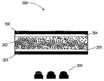
Figure 2- Light Scattering Display Cell
Figure 2 illustrates an embodiment of the present invention of a cell or pixel
200. (As described
further below, a display may be fabricated from a plurality of cells 200. Cell
200 may include three layers
including a top polarizer 201, a light scattering material 202 such as liquid
crystal dispersion systems (LCDS)
or other electro-optical scattering materials as previously discussed
hereinabove. For example light scattering
material may be a PDLC. Additionally, cell 200 may include a bottom polarizer
203. Top polarizer 201 may
be coated with a substantially transparent conductive material 204 such as
Indium-Tin-Oxide (ITO). Bottom
polarizer 203 may be coated with a substantially transparent conductive
material 205. Tn one embodiment, a
plastic or polymer may hold polarizers 201, 203 eliminating glass or other
substrates used in conventional
displays.
Returning to light scattering material 202, in an embodiment of the present
invention light scattering
material 202 may be configured to capture nematic liquid crystal into very
small droplets called "bubbles".
Once light scattering material 202 hardens, the bubbles are captured. Further,
light scattering material 202
may be configured to harden to form a gas fight bond between polarizers 201,
203. A PDLC composition that
may be used includes a commercially available liquid crystal BL035 available
from Merck Specialty by
Chemicals, Ltd. Poole, UK, dispersed in a ultraviolet (UV) curing epoxy MXM35
available from FFL
Funktionsfluid GmbH, Mainz-Hechtsheim, Germany. For example, in one such
composition that may be used
the epoxy and liquid crystal may be in the ratio of about thirty percent (30%)
epoxy to about seventy percent
(70%) liquid crystal.
Further, light scattering material 202 may be configured to harden to form a
bond between polarizers
201, 203. Moreover, by incorporating light scattering material 202 in cell
200, a liquid filling process as
required in prior art LCD displays may no longer be required. And, by
replacing LCD material with light
scattering material 202, the critical vacuum seal around the edges may be
eliminated.
Figure 2 also depicts a light source, LEDs 209, to illustrate the use of cell
200 in a display
configuration. LED's 209 may replace the flourescent light source used in
conventional LCD displays, and
eliminate the need for expensive color filters. Additionally, because LEDs may
be switched in conjunction
with the switching of electro-optical scattering material 202, a field
sequential color display may be fabricated
using a cell 200 in accordance with the present inventive principles.
Additionally, such operation eliminates
two-thirds of the number of data drivers that are otherwise needed in a
conventional LCD display as the same
driver may be used to exhibit all three colors (red, green and blue).
Additionally, this increases the aperture-
ratio of the pixel since cell 200 is not divided into red, green and blue sub-
pixels as in a conventional LCD
display. Additionally, the light source may be adjusted such that the light is
collimated prior to transmittal
through the cell. Tllis would reduce leakage of light at wide viewing angles
due to birefringent effects with
incoming light from an angle within a liquid crystal material in the light
scattering material.
CA 02489365 2004-12-09
WO 03/107130 PCT/US03/18762
In one embodiment, light scattering material may constitute a LCDS. It is
noted that light scattering
material may be any material capable of switching between a first state to a
second state where in the first
state, the light scattering material is substantially non-scattering in at
least the operable portion of the light
spectrum for which the display is to be used, and where in the second state
the light scattering materials is
substantially non-scattering in that portion of the spectrum. While it may
typically be the case that the
operable portion of the spectrum is the visible light spectrum, the present
inventive principles may be used
application in which at least one of the light sources is in the nonvisible
portion of the spectrum. A night
vision application, for example, xnay use an infrared liglit source.
Additionally, the transition of the light
scattering material between the first and second states (and vice versa) may
be substantially continuous as a
function of the voltage across the cell, whereby an amount of light scattering
also varies continuously. This is
described fiuther hereinbelow.
Contrast is achieved by the ratio of the maximum transmission - also referred
to as the bright ( optical
ON) state - through the display compared to the dark (optical OFF) state. When
the light scattering material is
substantially transparent, the incoming polarized light from the backlight and
first polarizes layer is
unaffected, substantially blocked by the front polarizes and the optical OFF
or dark state is achieved. When
the light scattering material is in its most scattering bright (optical ON)
state, the incoming polarized light is
scattered, which effectively depolarizes the light enabling transmission
through the front polarizes and the
optical ON or bright state is achieved.
As previously noted, a display device may incorporate a plurality of cells
200. Such a display may
include drive circuitry in conjunction with each cell to modulate the light
transmittance of the cell by
modulating the light scattering by the opto-electronic scattering medium.
Figure 3 illustrates a cell 300,
similar in configuration to cell 200 in Figure 2 and further including drive
circuitry associated therewith.
Polarizers 301 and 303, conductive material 304 and 305, light scattering
material 302 and light source 309 are
respectively similar to polarizers 201, 203, conductive material 204 and 205,
light scattering material 202 and
light source 209 in Figure 2. Drive electrodes include row .select 306, and
data line (or, equivalently, column
select) 307. As described in furthex detail below, electrodes 306 and 307 are
coupled to active element 308.
An active element may include an amorphous silicon (a-Si) tlun film transistor
(TFT), a polysilicon TFT, TFT,
a CdSe TFT or other switching device such as a metal-insulator-metal (MIM)
diode, or a metal oxide varistor
(MOV) as described in further detail hereinbelow. Electrodes 306, 307 may be
bonded directly to polarizes
303 since a plastic or polymer may hold polarizes 303. Hence, the need for
printed circuit boards (PCBs),
printed wiring boards (PWBs) or tape automated bonding (TAB) xnay be
eliminated. Further, since electrodes
306, 307 and active device 308 are located outside the cell gap, circuits 306,
307 may be configured to be
thicker than in prior art thereby allowing very long thick but thin traces of
the desired resistance. As
illustrated in Figure 3, active element 308 is placed inside the profile
allowing more surface area while
reducing the aspect ratio of cell 300 and permitting higher resolution pixel
display densities. As further
illustrated in Figure 3, cell 300 does not place any components inside the
critical cell gap (spacing between the
top and bottom electrodes) as in conventional displays. By not having
components inside the cell gap, cell
300 may be used to display materials such as supertwist nematic (STN), twisted
nematic (TN), cholesteric,
organic LED, electroluminescent (EL), electrophoretic ink (E-ink) and
electrophoretic paper (E-paper).
6
CA 02489365 2004-12-09
WO 03/107130 PCT/US03/18762
Another embodiment of a cell structure with more elements than cell 200 but
easier to manufacture with off
the-shelf components is discussed below in conjunction with Figure 4.
Fi~»re 4 - Alternative Embodiment of Cell that Allows Construction of a
Reflective Display Using Off the-
Shelf Components
Figure 4 illustrates another embodiment of a cell 400 incorporating the
principles of the present
invention that allows construction of a reflective display using off the-shelf
components. Cell 400 is
configured substantially the same as cell 300 (Figure 3) except polarizers
301, 303 (Figure 3) of cell 300 are
replaced with polymer or glass substrates 401, 402. Substrates 401, 402 may
each be coated with electrical
conductive material (404, 407, respectively). In one embodiment, substrate 402
may not be transparent.
Conductive material 404 may be transparent, e.g., ITO, and coating 407 may be
a solid conductive paint or
print. Substrate 402 may be dimensioned to hold active component 406. Color
element 403 may be added.
FiQUres 5 - Exploded Views
To further understand the configuration of display devices in accordance with
embodiments of the
present invention, refer now to Figure 5 illustrating in exploded views,
display devices 500 - 536, respectively.
Figure 5 illustrating in an exploded view, an embodiment of a display device
500 in accordance with
the present inventive principles. Display device 500 may be particularly
adapted for use with a metal oxide
varistor 530 (MOV) as the active device and a passive device 532 resistor.
Display device 500 includes top
and bottom polarizers, 502 and 504, respectively. An LED light source 506
including at least a tri-colored set
of LEDs (primary colors, red, green and blue) are disposed behind polarizer
504. Additionally a fourth, white
LED may also be included in light source 506. (It would be appreciated by
those of ordinary skill in the art
that the depiction of light source 506 is schematic, and that an backlight
embodiment would include a
multiplicity of LED devices for each color. The operation of a backlight that
may be used in conjunction with
the present inventive principles will be discussed further hereinbelow.) An
artisan of ordinary skill in the art
would recognize that bottom polarizer may be omitted if a polarized Iight
source is used. For example, laser
diode sources may be used to provide a polarized source. Alternatively, a
polarization mechanism may be
integrated with the LEDs. One such device is the ProFlux MicrowireTM polarizer
supplied by Moxtek, Inc.,
Orexn, UT. Note too that polarizer films need not be placed on the outside of
the substrate. Alternatively the
polarizers may be placed on the inner surface of the substrate, for example
using thin crystal filin (TCFTM)
polarizer technology as is available from Optiva, Inc., South San Francisco,
CA. Such placement may reduce
parallax.
Disposed between the top and bottom polarizers are an upper substrate 508,
opto-electronic light
scattering medium 510 and a lower substrate 512. Uppex substrate 508 may be
glass in an embodiment of the
present invention. Electrically conductive data lines 514 may be disposed on a
bottom surface of upper
substrate 508. Data lines 514 may be fabricated from ITO, for example, and the
grooves therebetween formed
by laser etching other etching methods scribing or printing. Lower substrate
512 provides a supporting
structure for the electronic components of the display device. These may
include row and column drivers 518
and 516, which are respectively coupled to select lines 522 and data lines
520, and mounted to the bottom
surface of lower substrate 512. Data lines 520 may be electrically coupled to
corresponding ones of data lines
514. Upper surface 524 of lower substrate 512 bears conductive coating 526,
which is segmented by grooves
528. Grooves 528 segment conductive coating 526 to form the device cells, and
constitute the lowex
7
CA 02489365 2004-12-09
WO 03/107130 PCT/US03/18762
electrodes thereof. Data lines 514 form upper electrodes of corresponding
display cells. Display device 500
also includes drivers for each cell, which may comprise active driver members
530 and passive driver
members 532. Active driver members 530 and passive driver members 532 may be
disposed within
corresponding holes 536 in substrate 512. Active driver members 530 may be MOV
devices, and passive
driver members 532 may be resistors. Active driver members 530 may be coupled
to corresponding ones of
select lines 522 and passive members may be coupled to corresponding ones of
data lines 520.
The interconnection of active members 530 and passive members 532 to form a
driver may be further
understood by referring to Figure 6 illustrating a schematic representation of
a driver 600 comprised of an
active member 530 and passive member 532. Capacitor 602 represents the
parasitic capacitance of a cell.
Node 604 corresponds to the electrical interconnnection between data lines 520
and data lines 514 described
hereinabove. Line 606 represents the electrical connection between passive
member 532 and active member
530 formed by conductive coating 526.
In operation, the active member provides a threshold for the electro-optic
scattering medium. To
matrix address a device, the device remains inactive for at least one-half the
applied voltage, Von. For
example, if the device is essentially fully on at the applied voltage Von~ it
is desirable to be fully off at O.SVon
Volts. In other words, the data voltage on data 522 voltage is at O.SVon
Volts, no other cell in the column can
turn on unless the voltage across the cell is Von ~rolts~ To turn the cell on,
the select or row voltage (on the
corresponding select 520) has to go to a negative value, or-O.SVon Volts. When
the data voltage is at ground
and the row voltage is at -O.SVon Volts the cell should not turn on.
It would be appreciated by those of ordinary skill in the art that a MOV can
be made to turn on at any
desired voltage, primarily by changing the thickness, which sets the distance
between the input and output
electrodes. An embodiment of the present invention, the MOV may be selected to
operate at the desired
threshold. For example, the MOV may be selected to have a turn-on voltage
(commonly referred to as the
MOV breakdown voltage) of about 5 volts. As shown in Figure 5, active members
530 are shown to be
located between the select electrodes and the bottom electrode of the cells.
Alternatively the active members
may be located between the top of the cell and the data electrodes.
The MOV active member also acts as a switch that will not let the cell
discharge. This allows the cell
to perform similarly to an active matrix device. Thus, the display does not
depend on average voltage to
opexate. The result is that the display performance may be similar to active
matrix displays.
FIGURE 7 illustrates an exploded view of another embodiment of a display
device 700 in accordance
with the principles of the present invention. Display device is similar to
device 500 of FIGURE 5 and
includes top polarizes 702, opto-electronic light scattering medium 710 and a
lower polarizes 712. Electrically
conductive top electrode 714 may be disposed on a bottom surface of polarizes
702. Lower polarizes 712 may
provide in the illustrated embodiment, a supporting structure for the
electronic components of the display
device which may include row and column drivers 716 and 718, which are
respectively coupled to select lines
720 and data lines 722. Additionally, lower polarizes 712 may form a light
channel for the light supplied by
LED light source 706. In an alternative embodiment, a lower substrate, similar
to lower substrate 512, Figure
5, may be used in conjunction with a lower polarizes, similax to bottom
polarizes 504, Figure 5, or
alternatively, a polarized light source.
8
CA 02489365 2004-12-09
WO 03/107130 PCT/US03/18762
LED light source 706 may include at least a tri-colored set of LEDs (primary
colors, red, green and
blue). Alternatively, LED light source 706 may also have a white LED (not
shown). The operation of display
device 700 is similar to that of display device 500. An active element 800
mounted on polarizer 712 may be
used as an alternative to active element 530 and passive element 532 shown in
FIGURE 5. Active element
800 uses only one hole 736 through polarizer 712.
Refernng to FIGURE 8, active element 800 may be a TFT or similar device
including a drain 801,
source 802 and gate 803. The corresponding structures are also illustrated in
Figure 7.
Figures 9A-9C - Operation of Field Sequential Color
The operation of a field sequential color display in accordance with the
present invention may be
further understood by referring to Figures 9A-9C. The generation of an image
frame starts in step 902 of
process 900 for generating a field sequential display in accordance with an
embodiment of the present
invention. Process 900 then enters a loop over sub-frames in step 904. For
purposes herein, a sub-frame may
be understood to be any portion of a complete frame of an image being rendered
on the display; the complete
frame being a composite of sub-frames. Commonly, field sequential color may be
perceived to constitute the
sequential display of three monochrome sub-frames in which all pixels of the
display are addressed in each
sub-frame. However, for the purposes herein, a sub-frame is not restricted to
be monochromatic illumination,
nor are the sub-frames necessarily three in number.
In step 906 the sub-frame is displayed. Step 906 will be described further in
conjunction with
Figures 9A and 9B (where, for clarity the alternative embodiments have been
labeled 906a and 906b,
respectively). If the current sub-frame is not the last sub-frame of the image
frame, process 900 returns to step
904 to continue looping over sub-frames. Otherwise a new frame starts in step
902.
Refer now to Figure 9B illustrating step 906 in further detail for a field
sequential color methodology
in accordance with an embodiment of the present invention.
In step 926, the sub-frame is addressed, whereby the illumination values are
stored in the pixels (or
equivalently cells) of the sub-frame.
In step 928 a delay may be employed. For example, a delay may be used to allow
time for the light
scattering material to reach a substantially stabilized state. Recall that
electro-optic light scattering materials
may be switched from a light scattering state to a substantially light
transparent state and a continuum of light
scattering states therebetween.
In step 930 the light source is flashed. The duration of the flash is
determined by several factors,
including but not limited to the sub-frame refresh rate, the addressing speed,
the response of the display
medium to a substantially stabilized state, and other human factors related
issues. These factors are
recognized to those skilled in the display art. And typical values may be in
the range of about 1 to about 20
ms.
Step 906a then continues with step 908, Figure 9A.
An alternative embodiment of a field sequential color display methodology in
accordance with the
present invention, which may be referred to a segmented field sequential color
(SFSC) is illustrated in Figure
9C (step 906b). Note that step 906a may be understood as a subset of step 906b
in which a sub-frame
comprises a single segment, or stated conversely, an SFSC having a single
segment.
In step 956 loop over segments is entered.
9
CA 02489365 2004-12-09
WO 03/107130 PCT/US03/18762
In step 958, the pixels corresponding to a segment are addressed. As described
further hereinbelow, a
segment may include a preselected subset of pixels whereby the entire display
constitutes the union of the
segments. In other words, the addressing in step 956 may address a portion of
the sub-frame.
In step 960 a delay may be employed. As previously noted, a delay may be used
to allow time for the
light scattering material to reach a substantially stabilized state. Recall
that electro-optic light scattering
materials may be switched from a light scattering state to a substantially
light transparent state and a
continuum of light scattering states therebetween.
In step 962, the light source is flashed. The duration of the flash is
determined by several factors,
including but not limited to the sub-frame refresh rate, the addressing speed,
the response of the display
medium to a substantially stabilized state, and other human factors related
issues. These factors are
recognized to those skilled in the display art. And typical values may be in
the range of about 1 to about 20
ms.
In accordance with the present inventive principles, a light source may be
designed to be a segmented
light source which may be used in conjunction with segmented addressing
described in step 956. For
example, in a typical three color (RGB) field sequential display, three light
color sources are switched "OFF"
while the specific color pattern is written to the entire sub-frame. Since a
typical display operates at 60 Hz or
16.66 milliseconds this leaves approximately 5.5 milliseconds per sub-frame.
This means that the display
drivers must operate 3 times faster than normal. However, this does not leave
any time to turn on the light
sources. Therefore, it is desirable to write to the entire display in 1
millisecond, leaving 4.6 milliseconds to
turn on the light source. This puts an even higher burden on the display
driver circuits to run 16 times faster.
By utilizing a segmented light source, the respective color light source
remains "ON" for most of the time,
approximately 5.5 milliseconds, and is only switched "OFF" during the time the
drivers are writing to the
pixels in the segmented sub-frame. If that segmented sub-frame constitutes 20
rows of a VGA display (640 x
480), as a further example, at 60 Hz frame rate this will be 16.66 ms/480/20
or 694.44 microseconds leaving
4.80 milliseconds for the light to be on. As discussed below, two benefits are
apparent from this approach.
First, the drivers can write at slower speeds. Second, the time the segmented
image frame is illuminated is
longer since the address time for a segmented sub-frame is less than the time
required to address a complete
sub-frame. This time difference is additional time the light source may stay
flashed on for the segmented sub-
frame.
To further appreciate SFSC, recall that steps 956-964 are inside the loop over
sub-frames (step 904,
Figure 9A). Thus within each of the sub-frames, each segment is addressed, and
therefore within each sub-
frame, all pixels (or equivalently cells) are addressed. However, for each
segment in successive frames, the
color of the light source flashed in step 962 need not be the same. In other
words, in the first frame, for a
given segment, the color of the light source flashed in step 962 may be a
first color, say red, for example. In
the next frame, the color of the light source flashed in step 962 may be a
second color, say green. Likewise, in
the next frame the color of the light source flashed for the segment may be a
third color, say blue, and so forth
if the display includes more that three colors. Additionally, in the current
frame, each segment in the loop
over segments may sequence through the colors comprising the light source.
To further understand an SFSC process in accordance with the present inventive
principles, consider
the following concrete example which further illustrates the previous
discussion of a segmented light source.
CA 02489365 2004-12-09
WO 03/107130 PCT/US03/18762
As stated above, a display in accordance with the present invention may be
divided into segments each
composed of n select lines or rows of pixels. For illustration suppose n is
five. At typical frame rates of about
120 Hz - 190 Hz each segment may be written in 1.1 milliseconds. For an XGA of
1024 columns X 1024
rows, each segment would be composed of 1024 /5 or approximately 205 lines or
rows.
To operate a conventional field sequential color (FSC), the entire 1024 lines
need to be written in less
than 3 milliseconds, leaving only 2.5 milliseconds for the backlight to add
color. This implies a writing speed
of about 2.9 microseconds per line or row.
In the SFSC process of the present invention, the segment is written in 1
millisecond leaving 4.5
milliseconds for the light source to add color, implying a writing speed 4.8
microseconds per row. The result is
slower writing speed (4.8us) for SFSC than for FSC (2.9us). Because the time
the segment is on is longer a
slower responding LCD or scattering material may be used.
Additionally because for the reason that sub-frame contains one-third of the
full color image frame
(for a three-color system) and it is harder for the eye to see changes in the
image as the extra one-third is
added each sub-frame. The result is that human eye sees less flicker and the
sub-frame rate may be reduced
from for example 120 Hz to about 25-30 Hz.
One of ordinary skill in the art would appreciate that the foregoing values
are illustrative and other
frame rates, resolutions, number of colors, etc. would give rise to different
values and all such embodiments
would fall within the spirit and scope of the present invention.
Step 906b then continues with step 908, Figure 9A.
Although the method and display device are described in connection with
several embodiments, it is
not intended to be limited to the specific forms set forth herein, but on the
contrary, it is intended to cover such
alternatives, modifications and equivalents, as can be reasonably included
within the spirit and scope of the
invention as defined by the appended claims. It is noted that the headings are
used only for organizational
purposes and not meant to limit the scope of the description or claims.
Figure 10 - Method of Manufacturing Display with MOV Active Elements
A method of manufacturing a liquid crystal device in accordance with the
current invention, using a
metal oxide varistor (MOV) as the active element, is shown in Figure 10. In
step 1005, top and bottom
polarizers are provided, such as 502 and 504 in Figure 3. These polarizers
have interior and exterior surfaces.
The interior of the top polarizes is coated with a conductive material, such
as ITO, in step 1010. A data
pattern is then etched into that conductive coating in step 1015. A light
scattering material is then deposited in
step 1020.
Drive electrodes and cell data and source electrodes are etched or printed
onto the exterior surface of
the bottom polarizes in step 1025. In step 1030, sets of first and second
holes are fabricated through the
bottom polarizes. In step 1035, metal oxide varistor active elements are then
printed or installed into the first
holes through the bottom polarizes so that one electrode of the active element
is resident to the interior surface
of the polarizes, but not pertruding past the plane of the interior surface.
In step 1040, passive elements are
printed or installed into the second holes through the bottom polaxizer so
that they are congruent to but not
protruding past the plane of the interior surface of the bottom polarizes. The
interior of the bottom polarizes is
coated with a conductive medium in step 1045. This conductive medium, shown as
526 in Figure 5, will make
11
CA 02489365 2004-12-09
WO 03/107130 PCT/US03/18762
an electrical contact between the active and passive electrical elements. In
step 1050, a cell pattern is etched
in the conductive material deposited in step 1045.
Step 1055 involves filling the electrode pattern on the exterior surface of
the bottom polarizes with
conductive ink, provided that this was not previously printed in step 1025. At
the intersection of the data and
source electrodes printed in step 1025, a crossover electrode pattern is
printed or masked on the exterior of the
bottom polarizes in step 1060. Subsequently, in step 1065, crossover
electrodes are printed or masked on to
the exterior surface of the bottom polarizes. The top and bottom polarizes
assemblies are then bonded together
in step 1070 and the data pattern on the top polarizes is interconnected with
the data electrode pattern on the
bottom polarizes in step 1075.
Figure 11 - Method for Manufacturing Display with Transistor Active Elements
An alternative method for manufacturing a liquid crystal device of the present
invention, using a
transistors as the active element, is shown in Figure 11. Top and bottom
polarizers are provided in the step
1105. These polarizers also compxise the top and bottom substrates and have
surfaces both interior to and
exterior to the cell. The interior of the top polarizes is coated with a
conductive material, such as ITO, in step
1110. A light scattering medium 510 is then deposited onto the coated interior
surface of the top polarizes in
step 1115.
Driver electrodes and cell and data source electrodes are etched or printed
onto the exterior surface of
the bottom polarizes 504 in step 1120. In step 1125, holes are fabricated
through the bottom polarizes, which
are then filled with a conductive material in step 1130. This conductive
material forms an electrical conduit
between the interior and exterior surfaces of the bottom polarizes. The
interior of the bottom polarizes is
coated with a conductive medium in step 1135, which makes an electrical
contact with the conductive material
filled into the holes in step 1125. A cell pattern is then etched into the
conductive material coated on in 1135,
if not previously printed in that step.
The electrode pattern on the exterior of the bottom polarizes is then filled
with conductive ink in step
1145, if this has not previously been done as part of step 1120. An electrode
crossover pattern is printed or
masked onto the exterior of the bottom polarizes at the intersection of the
data source electrodes, in step 1150
and then crossover electrodes are printed or masked on in step 1155. In step
1160, the active element
transistors are installed to make electrical connections between the row and
data electrodes and the electrical
conduits through the polarizes; this includes connections between data and
drain, gate and row, and source to
conduit. The two polarizes assemblies are then bonded to one another in step
1165.
Figure 12 - Method of Manufacturing Display Using Transistor Active Element By
Printing
Another alternative method of manufacturing a display device according to the
present invention,
using transistors as the active element, is shown in Figure 12. In step 1205,
a top polarizes is printed onto the
exterior surface of a substrate. The interior of that substrate is coated with
a conductive material, such as ITO,
in step 1210. Light scattering material is deposited onto the conductive
material in step 1215. The light
scattering material is then coated with a conductive material layer, such as
ITO, in step 1220.
12
CA 02489365 2004-12-09
WO 03/107130 PCT/US03/18762
In step 1225, a bottom substrate is then provided, onto which the bottom
polarizes is printed, holes
are masked or printed for pass-through conductors and a waffle pattern is
printed 1225. Driver electrodes and
cell data and source electrodes are printed onto the exterior surface of the
bottom polarizes in step 1230. The
holes through the bottom substrate are then filled with conductive material,
in step 1235, thus forming an
electrical conduit between the interior and exterior surfaces. An electrode
crossover pattern is then printed or
masked onto the exterior surface of the bottom substrate in step 1240, and
then crossover electrodes are then
printed or masked onto that substrate in step 1245. Active element transistors
are then installed in step 1250,
to make electrical connections among the row and data electrodes and
electrical conduits; this includes
connections between drain and data, gate and row, and source to conduit. The
top and bottom
substrate/polarizer assemblies are then bonded to one another in step 1255.
Figure 13 - Method of Modifying an Existing Display
It is also contemplated that one might wish to modify an existing liquid
crystal display to conform
with the present invention. Figure 13 discloses a method for modifying
existing liquid crystal display devices.
In step 1305, the existing LCD is disassembled by removing the top substrate
assembly, including the
polarizes, the conductive (ITO) layer, rubbing layer and color filter
(described in Figure 1). Up to two-thirds
of the transistors are removed from the bottom substrate assembly, along with,
optionally, the rubbing layer on
that substrate, in step 1310. Light scattering material is then coated onto
the interior surface of the bottom
substrate, in step 1315. The top substrate assembly is then reinstalled
including only the polarizes, the
substrate itself, and the conductive (ITO) layer, and optionally the rubbing
layer, in step 1320.
13