Note : Les descriptions sont présentées dans la langue officielle dans laquelle elles ont été soumises.
CA 02492499 2005-O1-11
WO 2004/008664 PCT/US2003/021715
METHOD AND APPARATUS FOR DIRECTLY MODULATING A LASER DIODE
USING MULTI-STAGE LASER DRIVER CIRCUITRY
FIELD OF THE INVENTION
The present invention is related to optical communications systems, and
particularly
to a method and apparatus for directly modulating a laser diode using mufti-
stage laser driver
circuitry.
BACKGROUND
In optical communication systems, laser diodes are typically used to generate
optical
signals for transmission, and laser drivers are typically used to modulate the
laser diodes.
One can encounter a number of problems when directly modulating a laser diode
using a conventional laser driver IC (integrated circuit), particularly in the
absence of
cooling. First, ringing and distortion of the drive current waveform may
result from one or
more of wire bond inductance, laser diode capacitance, and laser driver output
capacitance.
Second, it may be difficult to keep the laser diode temperature low enough for
adequate
performance because of heat generated by the laser driver IC, which should be
as close as
possible to the laser diode in conventional systems in order to minimize the
interconnect
inductance that may contribute to the ringing stated above.
Therefore, it is desirable to provide a method and apparatus for
interconnecting the
laser driver to the laser diode that can reduce waveform distortion and
ringing, while
reducing the effect of the heat generated by the laser driver on the laser
diode.
SUMMARY
In an exemplary embodiment according to the present invention, an optical
transmitter
is provided. The optical transmitter includes: a driver circuit capable of
receiving data and
applying the data to drive a laser diode; a transmission line having first and
second ends, the
first end being coupled to an output of the driver circuit; and an amplifier
having a first
terminal coupled to the second end of the transmission line and a second
terminal coupled to
the laser diode, wherein signal amplitude applied at the first terminal
controls an optical
output amplitude of the laser diode.
BRIEF DESCRIPTION OF THE DRAWINGS
These and other aspects of the invention may be understood by reference to the
1
CA 02492499 2005-O1-11
WO 2004/008664 PCT/US2003/021715
following detailed description, taken in conjunction with the accompanying
drawings,
wherein:
FIG. 1 is a block diagram of an optical communications system, in which an
exemplary embodiment according to the present invention ma.y be applied;
FIG. 2 is a schematic diagram of an optical transmitter in an exemplary
embodiment
according to the present invention;
FIG. 3 is a schematic diagram of an optical transmitter in another exemplary
embodiment according to the present invention; and
FIG. 4 is a schematic diagram of an optical transmitter in yet another
exemplary
embodiment according to the present invention.
DETAILED DESCRIPTION
In an optical transmitter, if the laser driver IC is interconnected to the
laser diode over
a transmission line, the laser driver IC does not need to be close to the
laser diode and heat
generated by the laser driver IC does not affect the laser diode temperature
as much as the
case where, for example, the laser driver IC is wire bonded to the laser
diode.
However, when a transmission line is used to interconnect the laser driver IC
to the
laser diode, impedance matching should typically be provided at both ends of
the
transmission line to prevent waveform distortion caused, e.g., by RF (radio
frequency)
reflections. If an impedance matching resistor is used in series with the
laser diode, the
voltage swing can be increased sufficiently to provide adequate modulation
current.
However, with a modulation current of 80 mApp (mini amps, peak-to-peak), the
voltage swing required to provide adequate modulation current in a 505, system
would be 4.0
Vpp (voltage, peak-to-peak), and in a 25SZ system would be 2.0 Vpp. Such large
voltage
swings require increased laser driver IC supply voltages and increase overall
system power
dissipation. The modulation current of 80 mApp, for example, may be required
at high
temperatures. At room temperature, a typical modulation current may be between
40 mApp
and 60 mApp. Further, bias current dissipated by the impedance matching
resistor may add
to power dissipation. The bias current typically varies with temperature, and
may, for
example, be between 10 mApp and 80 mApp.
In addition, it is generally necessary to back-terminate the laser driver IC
with a
matching impedance. This back termination can double the output current
requirement for the
laser driver. For example, in a 255 system with 80 mApp modulation required
for the laser
2
CA 02492499 2005-O1-11
WO 2004/008664 PCT/US2003/021715
diode, the laser driver may have to supply 160 mApp if half of the modulation
current is
consumed in the back termination..
Therefore, the overall system power dissipation is increased both by the need
for a
higher drive voltage swing and by the need for a reverse termination at the
laser driver. Since
reducing system power dissipation is desirable in uncooled optical transmitter
design, it may
not be desirable to use the transmission line interconnect between the laser
driver and the
laser diode, unless a solution to reduce the power dissipation can be devised.
Instead of using a transmission line between the laser driver IC and the laser
diode,
the laser driver IC may be mounted as close as possible to the laser diode to
minimize
l0 inductance. In this case, the heat generated by the laser driver IC should
be tolerated by the
laser diode. In this case where the laser diode and the laser driver IC are
mounted very close
to one another and coupled, for example, via wire bonding, a transmission line
is not used.
Hence, additional power dissipation (e.g., by impedance matching resistor(s))
associated with
using transmission line interconnect can be avoided.
However, the resonance of the interconnect wire bond with the laser
capacitance and
driver output capacitance can cause ringing. This ringing may be exacerbated
by the high
output impedance of conventional laser driver circuits.
Conventional laser drivers are typically designed using a differential output
stage with
a current source connected to the emitters or sources of the output
differential pair. The laser
driver output is generally taken from the collector or drain of one of the
output transistors,
and the collector or drain of the other output transistor is typically
terminated through a load
resistor to AC ground. The output impedance of the laser driver, as seen by
the laser diode
looking into the collector or drain of the output transistor, is relatively
high. This contxasts
with the dynamic impedance of the laser diode itself, which is generally only
a few ohms.
However, high impedance drivers are generally used at all bit rates because of
the ease of
design of high speed differential stages, and because of the ease and accuracy
of modulation
current control afforded by the current source that sets the tail current of
the differential pair.
However, the high output impedance.of the driver does not load down or damp
the
ringing caused by wire bond inductance, which may become severe at high bit
rates such as
10 Gbps (Giga bits per second). In order to reduce ringing, damping resistors
may be used
either in series between the laser diode and the laser driver, or in parallel
with the driver
output capacitance. A series resistor may have the detrimental affect of
increasing the drive
voltage requirement, and a parallel resistor may have the detrimental affect
of increasing the
3
CA 02492499 2005-O1-11
WO 2004/008664 PCT/US2003/021715
drive current requirement. In both of these cases, the total power dissipation
may be
increased.
Further, heat generated by the laser driver IC may cause the temperature of
the laser
diode to rise because of the close proximity of the laser driver to the laser
diode.
Conventional laser drivers at 10 Gbps typically consume between 0.5W (watts)
and 1.5W of
power. In order to reduce the rise in temperature due to the heat generated by
the laser driver
IC, a very low thermal resistance packaging is often used, which increases
system cost and
size.
Another problem introduced by having the driver IC very close to the laser
diode may
l0 come from passive components and. multiple interconnects typically used to
support driver
operation. These components and interconnects may increase the size and
complexity of the
laser package, thereby increasing cost and reducing possibilities for
miniaturization.
In an exemplary embodiment according to the present invention, a laser diode
is
directly modulated by a data signal. In this embodiment, laser driver
circuitry is split into at
least two separate stages separated by a length of electrical transmission
line. A first stage,
for example, may include a conventional laser driver. A second stage, for
example, may
include a transistor configured as an emitter follower or a source follower,
which is
implemented between the laser driver and the laser diode in an optical
transmitter.
This exemplary embodiment provides for reduced power supply voltage and power
dissipation as compared to an optical transmitter where a laser diode is
driven over a
transmission line between the laser driver IC and the laser diode without a
use of such
additional stage for laser driving. This reduction to required voltage and
power can be
attributed at least partly to the absence of using impedance matching
resistors) between the
laser driver IC and the laser diode.
Since a transmission line interconnect is used between the laser driver IC and
the laser
diode in the described embodiment, power dissipation and associated localized
heating in the
immediate vicinity of the laser diode can be reduced as compared to an optical
transmitter
having a conventional laser driver IC mounted very close to the laser diode.
In addition,
reduction to laser diode drive current ringing and distortion caused by
interconnect
inductance between the laser diode and laser driver can also be realized.
Further, by using
the transmission line interconnect, the number of passive components and
number of
electrical connections used inside the laser package can be reduced as
compared to the case
of having a conventional laser driver IC co-packaged with the laser diode.
4
CA 02492499 2005-O1-11
WO 2004/008664 PCT/US2003/021715
FIG. 1 is a block diagram of an optical communications system 10, in which an
exemplary embodiment according to the present invention may be applied. The
optical
communications system 10 illustrates a system with an optical transmitter 14
at the
transmission end of an optical communications medium 20 and an optical
receiver 22 at the
receiving end. However, those slulled in the art would appreciate that
practical
communications systems may have one or more optical transmitters as well as
one or more
optical receivers at each end of the optical communications medium. The
optical
communications medium 20 may comprise a fiber optic cable.
The optical communications system 10 includes a data source 12, which provides
data
l0 for modulating the laser output for optical transmission. The data from the
data source 12
may be encoded, for example, via forward error correction (FEC), for data
detection and/or
recovery at the receiving end. For example, the data may be provided as a high
data rate
(e.g., 10 Gbps or higher) Rf (radio frequency) signal. The data source, for
example, may be
coupled to a computer network for ,generating the data and providing the same
to the data
source 12.
The optical transmitter 14 includes laser driving circuitry 16 and a laser 18.
The laser
driving circuitry may be mufti-stage, and may receive one or more control
signals for
controlling various different parameters of the laser output, such as, for
example, modulation
amplitude and bias. The laser 18 may be a laser diode or any other optical
source suitable for
optical communications. It should be noted that the laser driver 16 (or a
portion thereof) and
the laser 18 may be packaged separately, and be coupled over a length of
transmission line in
an exemplary embodiment according to the present invention.
The transmission line, for example, may be co-planar or include a micro strip,
and
may be implemented on a circuit board and/or a flex circuit. For example, the
laser 18 and a
stage of the mufti-stage laser driving circuitry 16 may be included in a TO
(transistor outline)
can or other suitable laser package, and coupled to the remaining one or more
stages of the
laser driving circuitry 16 on a circuit board over a transmission line, which
may be on the
circuit board and/or the flex circuit.
The optical communications system 10 includes the optical receiver 22 and a
data
sink 24 at the receiving end of the optical communications medium 20. The
optical receiver
22, for example, may include one or more photodiodes for detecting the
received optical
signals and converting the optical signals to electrical signals.. The data
sink 24 may include
a decoder for decoding the data encoded at the transmission end. The data sink
24, for
5
CA 02492499 2005-O1-11
WO 2004/008664 PCT/US2003/021715
example, may be coupled to a computer network for distributing and/or
processing the
received data.
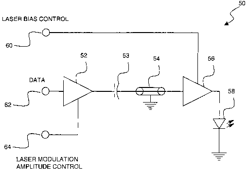
FIG. 2 is a schematic diagram of an optical transmitter 50 in an exemplary
embodiment according to the present invention. For example, the optical
transmitter 50 may
be used as the optical transmitter 14 of FIG. 1 in the exemplary optical
communications
system.
The optical transmitter 50 includes a laser driver 52 having variable output
amplitude.
The output of the laser driver 52 is applied at the input of an amplifier 56
through a capacitor
53 and over a transmission line 54. The amplifier 56, for example, may be a
fixed gain linear
amplifier (e.g., a fixed AC gain linear buffer amplifier), and may have
variable DC output
current. The output of the amplifier 56 is applied at the input of a laser
diode 58, which in
turn generates laser output corresponding to the output amplitude of the
amplifier 56.
In the exemplary optical transmitter of FIG. 2, the laser driver 52 directly
modulates
the laser diode 56 with a data signal 62. The laser driver circuitry is split
into at least two
separate stages separated by a length of the transmission line 54. The laser
driver 52 is the
first stage that generates a digital output that switches between two voltage
levels VO and V 1
corresponding to whether the input data consists of a "zero" or a "one". The
voltage levels
VO and V 1 may be determined by a laser modulation amplitude control signal
64, which may
allow the correct modulation amplitude to be applied to the laser diode 56 to
maintain its
desired operating point and extinction ratio (ratio between the optical "one"
and "zero"
levels).
The output from the laser driver 52 is coupled via a DC-blocking capacitor 53
to the
transmission line 54 and thence to the amplifier 56. In other embodiments, the
capacitor 53
may not be used. The amplifier 56 may be a constant gain, linear amplifier
that serves to
provide impedance matching to the impedance of transmission line 54 and also
provide
current gain prior to driving the laser diode 58, as the dynamic impedance of
a typical edge-
emitting laser diode is in the range of 5 to 10 Ohms, whereas the impedance of
typical
transmission lines is in the range of 25 to 50 Ohms. The amplifier 56 may also
provide a DC
bias current to the laser diode 58, which may typically be controlled by a
laser bias control
signal 60, which may be adjusted to maintain a constant optical output power
level.
A fixed-gain linear amplifier can generally be very simple, possibly only a
single
transistor. Hence, fixed-gain linear amplifiers can operate with lower
voltages and currents
than conventional laser drivers currently in use. These lower voltages and
currents allow for
6
CA 02492499 2005-O1-11
WO 2004/008664 PCT/US2003/021715
low added power dissipation in the vicinity of the laser diode. This low added
power
dissipation may simplify laser package design, as provision of adequate heat
sinking to
maintain low laser diode operating temperature is one of the major design
challenges for
products such as 10 Gb/s (giga bits per second) optical transceivers and
transponders. In
addition, reduced operating voltage may allow for reduction in laser driver
supply voltage.
This potentially reduces or eliminates a need for providing higher supply
voltage, which is
commonly required by conventional transceiver or transponder circuitry.
Further, a fixed-gain linear amplifier can be very simple and may require very
little
space and few electrical connections. It can be co-packaged with the laser
diode in a small,
to low-cost package such as a TO can. In addition, the fixed gain linear
amplifier can be
realized using a single-transistor common drain or common collector stage.
These and other
single-transistor configurations may provide low input capacitance, which
would provide
high frequency impedance matching to the transmission line 54. They may also
provide
current gain to reduce the drive voltage needed from the laser driver 52.
Further, they may provide low output impedance, which would help to damp
ringing
in the electrical drive signal provided to the laser diode 58. The ringing,
for example, may
result from one or more of the output capacitance of the amplifier 56, the
parasitic
capacitance of the laser diode 58, and the parasitic inductance between the
amplifier 56 and
the laser diode 58.
2o In another exemplary embodiment, an additional amplifier may be added
between the
laser driver 52 and the capacitor 53. The additional amplifier, for example,
may be a fixed
gain inverting linear amplifier. The additional amplifier may be useful when
the optical
transmitter employs a "dual loop" control circuit configuration (i.e. a
constant extinction ratio
control loop as well as the standard constant optical power control loop).
Such "dual loop"
control circuits often employ a small-amplitude, low frequency dither-tone
modulation of the
"ones"-level laser drive current which is then sensed by a monitor photodiode
and used to
estimate the modulation slope efficiency of the laser diode. The estimated
modulation slope
efficiency may then be used to adjust the laser modulation amplitude to
maintain a constant
extinction ratio.
3o Modulation of the "ones" level current may be accomplished by modulating
the tail
current of a differential pair of high-speed bipolar or N-channel FET
transistors that form the
output stage of the driver. If one of the differential outputs of such a
driver is directly
coupled to a laser diode, then low-frequency dither-tone modulation of only
the optical
7
CA 02492499 2005-O1-11
WO 2004/008664 PCT/US2003/021715
"ones" level may be accomplished. It may be undesirable to modulate the
"zeros" level
because this level is close to the diode's lasing threshold and modulation
near this point may
result in high levels of turn-on fitter.
Further, a problem may arise if a linear buffer amplifier such as those
described
previously is employed between a dual-loop digital driver and a laser diode.
The problem
comes from the inversion of the "one" and "zero" levels, such that the dither
tone modulation
from a typical dual-loop driver would show up on the "zeros" level rather than
the "ones"
level. This problem can be rectified if the additional amplifier (e.g.,
inverting linear
amplifier) is employed between the dual-loop laser driver 52 and the amplifier
56 that is
to connected to the laser diode. The inverting amplifier may be integrated
into either the laser
driver 52 or the additional amplifier, but in order to minimize power
dissipation close to the
laser diode, it may be more desirable to integrate it with the laser driver
52.
In other embodiments, a monitor photodiode may be used to monitor the output
of the
laser diode 58. The monitored signal may be used as a feedback signal to
control laser
modulation and/or bias. The monitor photodiode, for example, may be
implemented in the
same TO can as the laser diode 58 and/or the amplifier 56.
FIG. 3 is a schematic diagram of an optical transmitter 100 in an exemplary
embodiment according to the present invention. For example, the optical
transmitter 100
may be used as the optical transmitter 14 of FIG. 1 in the exemplary optical
communications
system. In the optical transmitter 100, the amplifier is implemented using a
single FET (field
effect transistor) (e.g., PHEMT (pseudomorphic high electron mobility
transistor)) configured
as a DC-coupled common drain amplifier. In other embodiments, a bipolar
transistor (e.g.,
an NPN bipolar transistor) may be used as a common collector amplifier. In
still other
embodiments, other transistors known to those skilled in the art may be used.
The optical transmitter 100 includes a laser driver 102 and a laser diode 108.
The
laser driver 102 receives data 124, and uses this data to modulate the laser
diode 108. The
data 124, for example, may have a data rate of 10 Gbps or higher. The laser
driver 102 also
receives a laser modulation amplitude control input 122, which can be used to
control the
peak-to-peak amplitude of the laser diode output.
3o In the exemplary embodiment, the laser driver 102 drives a transistor 106
through a
length of transmission line 104. The transmission line 104 may be implemented
on a circuit
board and/or a flex circuit as a co-planar transmission line or a micro strip.
The length of the
transmission line 104 may be on the order of 1.25 cm (centimeter), and may
vary between
8
CA 02492499 2005-O1-11
WO 2004/008664 PCT/US2003/021715
approximately .25 cm to a few centimeters. A capacitor 118 is placed between
the drain of
the transistor 106 and ground. The capacitor 118 may include two capacitors in
parallel, one
with small capacitance (e.g., 60 to 100 pf) in the TO can of the laser diode
108, and one with
larger capacitance (e.g., 0.1 ,u f) outside the TO can.
The optical transmitter 100 further includes a load resistor 110, which
provides a DC
(direct current) load for the laser driver 102. The load resistor 110 also
provides a reverse
termination for the transmission line 104, thereby enabling a substantial
matching between an
output impedance of the laser driver 102 and the characteristic impedance of
the transmission
line 104. In the optical transmitter 100, a capacitor 116 and an inductor 120
form a bias tee
io network, so that DC bias control of the transistor 106, and thereby of the
laser diode 108 can
be achieved through a laser bias control signal 126 applied to the gate of the
transistor 106
through the transmission line 104 and the inductor 120. The capacitor 116
provides DC
blocking to isolate the output of the laser driver 102 from the laser bias
control signal 126.
An impedance matching resistor 114 should be selected such that it provides
the
required terminating impedance for the transmission line 104, thereby enabling
a substantial
matching between an input impedance of the transistor 106 and the
characteristic impedance
of the transmission line 104. Those skilled in the art would appreciate the
values for various
different electrical circuit components, such as, capacitors, resistors and
inductors, for proper
impedance matching and operation of the optical transmitter circuitry.
2o The transistor 106, which may be replaced by an NPN bipolar transistor
configured as
an emitter follower, provides a relatively high input impedance which does not
load down the
output of the transmission line 104. An output from the transistor's source or
emitter, which
is connected to the laser diode 108, provides a low impedance drive signal for
the laser diode
108, which may damp ringing created by parasitic inductance between the
transistor 106 and
the laser diode 108. This way, one of the difficulties (i.e., ringing) with
previous
implementations of driver and laser diode interconnection can be resolved.
The exemplary embodiment results in a reduction to the required supply voltage
Vcc
because no resistor is used in series with the laser diode 106. The worst case
peak voltage
across the laser diode 106 under maximum current conditions, for example, may
be as high a
2.OV. If the supply voltage Vcc is 3.3V, for example, there would be 1.3V
remaining as the
collector-to-emitter voltage for the transistor 106, which is adequate for an
acceptable
transistor operation.
Further, with a typical laser dynamic impedance of 7S~ and a worst-case
modulation
9
CA 02492499 2005-O1-11
WO 2004/008664 PCT/US2003/021715
current of 80 mApp (milk-amps peak-to-peak), the AC voltage swing at the anode
(coupled
to the emitter of the transistor 106) of the laser diode 108 is 0.56 Vpp. For
a typical single-
transistor follower voltage gain of 0.5, the output voltage swing required
from the laser driver
102 is then 1.12 Vpp. This voltage swing is much less than the 2.0 Vpp or 4.0
Vpp needed for
the case where, for example, the laser diode 108 were driven directly over the
transmission
line 104 through an impedance-matching resistor without using a transistor.
Therefore, the reduced voltage swing required from the laser driver 102 plus
the low
Vcc requirement of the follower stage make it possible to design an uncooled
optical
transmitter with lower supply voltage and hence reduced overall power
dissipation compared
to to the case where the laser diode is driven directly from a transmission
line via the impedance
matching resistor.
Further, compared to having the laser driver IC very close to the laser diode,
the
power dissipation and hence heating close to the laser diode is reduced as
well. For example,
a conventional differential driver supplying 80 mApp of modulation current to
the laser and
operating from a supply voltage of 3.3V would result in a power dissipation of
80 mA x 3.3
V = 264 mW from just the modulation current alone. A typical driver would add
an
additional few hundreds of milk-watts for additional internal gain stages and
other functions.
For the same modulation current of 80 mApp, the average power dissipation with
the
transistor of the described embodiment is only 40 mA x 3.3 V = 132 mW because
the
modulation current is zero half of the time. The single-ended nature of the
follower driver
halves the modulation-associated power dissipation that is in close proximity
to the laser
diode 108. In addition, the laser driver 102 can be located remotely from the
laser diode 108
to minimize its heating effect.
An added benefit is that because the required current swing from the laser
driver 102
is reduced, there are additional power savings. For example, to achieve the
needed 1.12 Vpp
drive for the transistor 106 when driving a 5052 load plus a 5052, reverse-
terminating resistor,
the driver current needed is 1.12V/2552 = 44.8 mA. The modulation-associated
power
dissipation of the laser driver 102 is then 44.8mA x 3.3V = 147.8mW. The total
modulation-
associated power dissipation of the transistor 106 plus the laser driver 102
is then 147.8mW +
132mW = 279.8 mW, which is only slightly more than the power of 264 mW
required if the
laser driver 102 drove the laser diode 106 directly.
Therefore, with virtually no increase in total power dissipation, the
transistor 106 can
be used to substantially reduce the power dissipation in the immediate
vicinity of the laser
CA 02492499 2005-O1-11
WO 2004/008664 PCT/US2003/021715
diode. This reduced power dissipation can greatly simplify the thermal design
and cost of the
laser package. In addition, because the transistor 106 requires very few
passive components
and external connections, it can be co-packaged with the laser diode 108 in a
very small
housing with a small number of external electrical connections. In other
embodiments, a
resistor may be added between Vcc and the drain of the transistor 106 so as to
reduce power
dissipation at the laser diode (e.g., in the TO can).
In another exemplary embodiment, an additional inductor may be coupled to the
source of the transistor 106 to provide a path for laser diode bias current in
addition to the DC
current provided by the transistor 106. The other end of the additional
inductor may be
to coupled to a laser bias control signal. Using this configuration, the DC
current to be
delivered by the transistor 106 may be lowered. Hence, the overall power
dissipation and
associated heating in the neighborhood of the laser diode 108 may be lowered.
Additionally a capacitor may be added between the additional inductor and the
source
of the transistor 106. Further, another inductor may be placed between the
source of the
transistor and ground. This way, the DC voltage drops across the transistor
106 and the laser
diode 108 are not added in series, so that each device may have a full supply
voltage
available for its individual operation. This configuration may be useful in
designs where
supply voltages are reduced, for example, to 1.8V or 1.2V (from 3.3V for
example), which
may not provide enough operating voltage if the transistor 106 and the laser
diode 108 were
2o directly connected in series.
In another exemplary embodiment, an impedance matching resistor may be added
between the base of the transistor 106 (e.g., NPN bipolar transistor in common
collector
amplifier configuration) to the positive supply voltage Vcc, which may be
3.3V. In this case,
the impedance matching resistor and the resistor 114 should be chosen such
that their parallel
combination enables substantial matching between an input impedance of the
transistor 106
and the characteristic impedance of the transmission line 104. By using two
impedance
matching resistors, their values may be higher than if only a single
terminating resistor (e.g.,
resistor 114) were used. Hence, they would draw lower current for a given base
voltage,
which may translate into a reduction in overall power dissipation.
Further, in yet another exemplary embodiment, the transistor 106 may be
replaced by
an NPN bipolar transistor configured as a common emitter amplifier rather than
a common
collector amplifier. In other words, the laser diode 108 may be placed between
the positive
power supply Vcc and the collector of the NPN bipolar transistor rather than
between the
il
CA 02492499 2005-O1-11
WO 2004/008664 PCT/US2003/021715
emitter of the NPN bipolar transistor and ground. This way, lower drive
voltage may be used
for the same laser modulation current swing. However, it may result in a
higher effective
input capacitance for a given transistor, and of high output impedance which
may limit its
ability to damp ringing of the laser diode drive current waveform. When the
FET (e.g.,
PHEMT) is used, the transistor 106 may also have a common source
configuration.
The optical transmitter 150 of FIG. 4 is identical to that of the optical
transmitter 100
of FIG. 3, except that a capacitor 154 is connected in series with resistor
114, and the
inductor 120 is replaced with a resistor 152. The addition of the capacitor
154 allows the
circuit node at the gate of the transistor 106 to have a high DC impedance to
ground. Hence
there is only a small current required from the laser bias control circuit and
the inductor 120
can be replaced by the resistor 152.
Elimination of the inductor 120 allows for improved high frequency performance
because practical inductors generally have large parasitic capacitance that
limits the range of
frequencies over which they present a high impedance to the transmission line
104. A
resistor can provide a high impedance over a much wider frequency range than
an inductor,
hence allows fox a simpler and less expensive design.
As is the case for the optical transmitter 100 of FIG. 3, the transistor 106
of the optical
transmitter 150 may be replaced by a bipolar transistor (e.g., NPN bipolar
transistor) or any
other suitable transistor known to those skilled in the art.
In another exemplary embodiment, the optical transmitter 150 of FIG. 4 may
include
additional components. For example, a resistance may be added in parallel to
the capacitor
154, i.e., from a node between the resistor 114 and the capacitor 154 to
ground. Further, a
parallel resistor and capacitor (a parallel RC network) may be added between
the capacitor
116 and the transmission line 104. This way, the capacitor 154 may have a
smaller value,
and hence a smaller physical size, than for the configuration in FIG. 4.
For example, for the optical transmitter 150 in FIG. 4, the capacitor 154 may
have a
typical value of 0.1 ,u f (micro farad). With the addition of the
aforementioned capacitor and
the resistors, the capacitor 154 may have a value of 100 pf (pico farad). With
typically
limited space available in a laser package such as a TO can, this difference
in capacitor size
may be helpful in implementing a practical design.
For example, the parallel RC network between the capacitor 116 and the
transmission
line 104 may provide equalization to maintain an overall flat frequency
response even though
the capacitor 154 has only a small value. The resistor in parallel to the
capacitor 154 should
12
CA 02492499 2005-O1-11
WO 2004/008664 PCT/US2003/021715
be chosen to have a sufficiently high value that a resistor 152 may still be
used rather than an
inductor. Flat frequency response may be maintained if the resistor in the
parallel RC
network is chosen to be equal in resistance to the resistor in parallel to the
capacitor 154 and
the capacitor in the parallel RC network is chosen to be equal in capacitance
to the capacitor
154.
As is the case for the optical transmitter 150 of FIG. 4, the transistor may
be replaced
by a bipolar transistor (e.g., NPN bipolar transistor) or any other suitable
transistor known to
those skilled in the art.
Although this invention has been described in certain specific exemplary
embodiments, many additional modifications and variations would be apparent to
those
skilled in the art. It is therefore to be understood that this invention may
be practiced
otherwise than as specifically described. Thus, the present embodiments of the
invention
should be considered in all respects as illustrative and not restrictive, the
scope of the
invention to be determined by the appended claims and their equivalents.
13