Note : Les descriptions sont présentées dans la langue officielle dans laquelle elles ont été soumises.
CA 02492925 2005-O1-18
Z
DESCRIPTION
COPPER ALLOY, MET'~iOD OF MANUFACTURING COPPER ALLOY,
COMPOSTf'E COPPER MATERIAL AND METHOD OF MANUFACTURINCr
COMPOSITE COPPER MATERIAL
Technical Field
The present invention relates to a copper alloy and a composite copper
material that are suitable for wiring connectors of electric vehicles or the
like and
electrode materials for welding, and methods of manufacturing the copper alloy
and
the composite copper material.
Background Art
With the increasing EV (electric vehicle) design of automobiles, the
consumption of harnesses and connectors that are connection pants of wires
tends to
increase. In the adoption of EVs, ensuring safety. and gas mileage by
electronic
control techniques is also a purpose.
Connectors that are incorporated in automobiles are used in severe
environments of high temperature and vibration and, therefore, the reliability
of
connection and contact stability are required. Also, with increasing adoption
of
EVs, copper-based materials that have small energy losses, i.e., high
conductivity are
desired.
Also for electrode materials for welding, properties having values above
prescribed ones are required in all respects of mechanical ,strength, thermal
properties
and electrical properties.
For mechanical strength, it is known as the Hall-Fetch law that mechanical
strength is generally improved by refining the crystal structures of metal
materials.
CA 02492925 2005-O1-18
For example, when metal or alloy materials are deformed, material strength
increases due to work hardening. This is understood as follows. That is,
vazious
kinds of defects (point defect, dislocation, stacking fault, etc.) are
accumulated in
materials due to working (plastic deformation), and as a result of the
interactions of
these defects, the introduction and migration of new defects become difficult
and the
materials obtain resistance to external force.
To apply plastic deformation (strain) to metal materials, extrusion, drawing,
shearing, rolling, forging, etc, have hitherto been carried out. Concretely,
the H1P
(High Pz~ssure Torsion) process that involves twisting a material while
applying high
pzessure to the material, the CEC (Cyclic Extrusion Compression) process that
involves repeatedly threading a material through a constricted pipe, and the
ARB
(Accumulative Roll Bonding) process that involves cutting a metal sheet the
thickness of which has been reduced by rolling and repeatedly rolling
superimposed
metal sheets have been proposed, and in particular, as a concrete method of
refining
the grains of an aluminum alloy, the ECAE (equal-channel-angular extrusion)
process that involves applying shearing deformation to a material by lateral
extrusion
without a reduction of sectional area of the material has been proposed as
disclosed
in the Japanese Patent Laid-Open No. 9-137244, the Japanese Patent Laid-Open
No.
10-258334, the Japanese Patent Laid-Open No. 11-114618, the 3apanese Patent
Laid-Open No. 2000.271621, etc.
On the other hand, for copper alloys, methods disclosed in the Japanese Patent
Laid-Open No. 11-140568, the Japanese Patent Laid-Open No. 2000-355746, etc.
have been proposed. In these conventional techniques, to improve the
properties
(machinability and dezincification corrosion) of brass (Cu-Zn) that is used as
a
material for water faucet fittings and the like among other copper alloys,
dynamic
recrystallization is caused to occur by hot extrusion thereby to obtaizi the
refinement
CA 02492925 2005-O1-18
- 3 -
of crystal grains and specific ratios of crystal structures (ratios of the a,-
phase,
~3-phase and y-phase).
Also, to bring out prescribed properties from age-hardening type copper
alloys to which an element that does not dissolve or scarcely dissolves in a
solid
solution state at room temperature, such as chromium (Cr), zirconium (Zr),
beryllium
(Be), titanium (Ti) and boron (B), is added, this element is first caused to
dissolve
sufficiently in a solid solution sate at a high temperature and then quenched
and
brought to a supersaturated condition, which is followed by aging treatment at
a
pzescribed temperature, thereby causing the added element in a supersatuzated
condition to precipitate.
Even when the above-described work aging or aging treatment for aluminum
alloys and copper alloys is applied as it is to age-hardening type copper
alloys to
which an element, suclx as chromium (Cr), airconium (Zr), beryllium (Be),
titanium
(Ti) and boron (B), is added, it is impossible to simultaneously satisfy all
respects of
mechanical strength, thermal properties and electrical properties.
That is, in order to ensure that the thermal properties and electrical
properties
required of connectors used in electric vehicles or the like, electrode
materials, etc.
are developed, it is netessary to ensure that an added element that dissolves
in a solid
solution state is caused to precipitate in the largest possible amount. In
order to
cause this element to precipitate in a large amount, it is necessary to raise
the aging
temperature. However, when the aging temperature is raised, grain growth
proceeds and mechanical properties decrease. That is, mechanical strength and
thermal and electrical properties are in a tradeoff relation.
For thermal properties and electrical properties, copper alloys in which an
oxide such as alumina is dispersed in the copper matrix are excellent in
electrical
Conductivity and heat resistance and, therefore, these copper alloys are
widely used
CA 02492925 2005-O1-18
-- 4 -
in materials for electric parts. Many proposals to improve the properties and
manufacturing methods of these copper alloys have been made.
For example, a proposal has been made to improve electrical conductivity and
softening properties by adding, as elements that perform internal oxidation,
not only
aluminum, but also tin as a third element. (Japanese Patent Laid-Open No.
S9-150043)
There has been proposed a copper alloy in which the amount of particles of
not more than SO ~.~m is not less than 70 wt% owing to the use of a copper
alloy
powder of not more than 300 N.m which is manufactured by the atomizing process
and in which a readily oxidizing metal such as aluminum is caused to dissolve
ixx a
solid solution state. (Japanese Patent Laid-Open No. 60-141802)
There has also been proposed a method that involves internally oxidizing a
Cu-Al alloy powder thereby to convert Al to AlzO;, making the surface of this
alloy
powder smooth, green compacting the powder to form a green compact, and hot
forging this green compact at 600 to 1,000°C. (Japanese Patent Laid-
Open No.
63-241126)
Also, there has been proposed a method that involves internally oxidizing a
plate-like copper alloy containing A1 to convert Al to A12O3, working this
plate-like
alloy in coil form, sealing this coiled alloy in a metal tube, and hot wozking
this
metal tube at 900°C in a desired shape. (Japanese Patent Laid-Open No.
2-38541)
Also, there has been proposed a method that involves filling an alloy powder
obtained by internally oxidizing Cu-A1 alloy chips in a carbon die and hot
pressing
the alloy powder at 900°C and at a pressure of 400 kg/cmz. (Japanese
Patent
Laid-Open No. 2-93029)
l~rthermore, there has been proposed a method that involves improving
sintezability by causing an annular hard layer of A1203 to be present in the
interior of
a Cu-A1 alloy powder. (Japanese Patent Laid-Open No. 4-80301 )
CA 02492925 2005-O1-18
- 5 -
In all of the above-described conventional techniques, hot working at high
temperatures is performed and, therefore, structures tend to become coarse due
to
grain growth. Thus, in the conventional methods, it is impossible to obtain
materials that simultaneously satisfy, es the properties required of
connectors of
electric vehicles and electrode materials for welding, the requirements that
hazdness
be not less than 30 HRB, preferably not less than 40 IiRB, that electrical
conductivity be not less than 85 IACS%, preferably not less than 90 IACS%, and
that
thermal conductivity be not less than 350 W/(nn~lC), preferably not less than
360
W/(m-K).
When hardness is not less than 30 HRB, it is possible to prevent the tip of an
electrode material from becoming deformed and generating heat. When electrical
conductivity is not less than 8~ IACS%, it is possible to prevent an electrode
material
from reacting with a steel sheet and sticking to the steel sheet. When thermal
conductivity is not less than 350 W/(m~K), it is possible to prevent the
deposition of
an electrode nnaterial during welding because the cooling efficiency
increases.
Because A1243 does nat dissolve in Cu irA a solid solution state even at a
high
temperature, a conventional technique by which Alzp3 is caused to precipitate
by
aging treatment after dissalutaon in a solid solution cannot be applied to a
Cu-Al
alloy.
Disclosure of the Invention
A material that simultaneously satisfies all of the mechanical strength,
thermal
properties and electrical properties required of a material for connectors
used in the
wiring of electric vehicles or an electrode material for welding is obtained
by
ensuring that a second element that dissolves in s solid solution state at a
high
temperature, but does not dissolve or scarcely dissolves in a solid solution
state
(cannot maintain a solid solulioz~ state) at room temperature is caused to
dissolve in a
CA 02492925 2005-O1-18
- 6 -
base-material metal (Cu) in a solid solution state, that crystal grain
refinement is
achieved by applying a strain equivalent to an elongation of not less than
200% to
this material, and that this material is subjected to aging tceatnnent
simultaneously
with or after the application of this strain, thereby to promote precipitation
of the
second elennent among crystal grains.
Concretely, in a copper alloy containing a second element that does nat
dissolve or scarcely dissolves in a solid solution state at room temperature,
it is
possible to obtain a copper alloy the average grain size of which is not mote
than 20
pen and in which the second element precipitates among crystal grains. This
copper
alloy has a hardness of not less than 30 HRB, an electrical conductivity of
not less
than 85 IACS%, and a thermal conductivity of not less than 350 W/(m-K). The
second element is any of chromium (Cr), zirconium (Zr), beryllium (Be),
titanium
(Ti) and baron (B).
Extension, drawing, shearing, rolling or forging can be considered as means
for applying a strain to the material and conditions for the extrusion are
such that
lateral extrusion is performed at a die temperature of 400 to 500°C and
an. extrusion
speed of 0.5 to 2.0 mm/sec. It is also possible that before a strain is
applied to the
material, the material is subjected to aging treatment beforehand.
On the other band, in order to obtain a material that simultaneously satisfies
all of the mechanical strength, thermal properties and electzical properties
from a
ceramic powder (alumina or titanium boride) that does not dissolve in copper
in a
solid solution state even at a high temperature, a copper powder and a ceramic
powder are mixed together, thereby to form a mixed powder as a primary shaped
body, and a strain is applied to this primary shaped body, thereby to form a
secondary shaped body m which base material and ceramic particles are combined
together with refined particle sizes. As a result of this, a composite copper
material
having a hardness of not less than 60 HR.B, an electrical conductivity of not
less than
CA 02492925 2005-O1-18
7
85 IACS%, a thermal conductivity of not Iess than 350 W/(m-K); and a hardness
of
not less than 30 HRB is obtained.
Incidentally, as the means far applying a strain, for example, lateral
extrusion
is performed at a material temperature of not less than 400°C but not
more than
1,000°C and a die temperature of not less than 400°C but not
more than 500°C.
Why the specified raw material temperature is 400°C to 1,000°C
is that if the raw
material temperature is less than 400°C, extrusion becomes difficult
because of large
deformation resistance and sufficient bonding strength cannot be obtained
between
the parent phase (matrix) and particles and that if the raw material
temperature
exceeds 1,000°C, this temperature exceeds the melting point of copper
and copper
melts, making it impossible to apply a strain. The reason why the specified
die
temperature is 400°C to 500°C is that if the die temperature is
too low, extrusion
becomes difficult and if die temperature is too high, the die itself becomes
annealed.
The primary shaped body can be obtained by green compacting or by filling
the mixed powder in a tube. Furthermore, the average paxticle size of the
cerauric
powder is 0.3 to 10 p,m, a strain applied to the primary shaped body is
equivalent to
an elongation of not less than 200%, the avexage particle size of a base
material of
the secondary shaped body to be obtained is not more than 20 Vim, and the
average
particle size of ceramic particles is not more than 500 nm.
As described above, because titanium boride is not mixed with a copper
power and instead, a titanium powder that becomes titanium boride as a result
of a
reaction and a boron powder are formed in the copper matrix, it is possible to
increase mechanical strength as fine particles. Therefore, in another aspect
of the
invention, a method of manufacturing a composite copper material in which
titanium
boride is dispersed in the copper matrix comprises the following steps [1] to
[3j:
[1] the step of mixing a copper powder, a titanium powder and a boron
powder together, thereby to form a primary shaped body;
CA 02492925 2005-O1-18
[2] the step of giving thermal energy to the primary shaped body, thereby
causing the titanium powder and the boron powder to react with each other in
order
to form titanium bozide in a copper matrix; and
[3] the step of applying a strain to the pzxmary shaped body in which the
titanium boride is formed by plastically defozm.ing the primary shaped body,
thereby
to form a secondary shaped body.
For example, if the avezage grain size of a titanium powder and a boron
powder is 0.3 to 10 ~.m, it can be ensured that the average particle size of a
base
material of the secondazy shaped body to be obtained is not more than 20~m,
and
that the average particle size of titanium boride particles is not more than
400 nm,
and hence it is possible to obtain a composite copper material having small
deformation by pressurization during welding as an electrode rxiaterial for
welding
(due to low compressive strength of the material).
Part of titanium and boron dissolve in copper in a solid solution state when
thermal energy is applied to the primary shaped body. However, if the titanium
and
boron in this solid solution state remain in an unreacted condition, the
composite
copper material is inferior in electrical conductivity and thermal
conductivity.
Therefore, it is preferred that the secondary shaped body be subjected to heat
treatment in the same step as the step of applying a strain by plastic
deformation or a
step following this step, whereby the unreacted solute elements (titanium and
boron)
are caused to precipitate.
The means for applying plastic deformation, the material temperature, the die
temperature, the extrusion speed and the number of times of extrusion are the
same
as described above.
Bzref Description of the Drawings
CA 02492925 2005-O1-18
_ g _
Figure 1 is a drawing to explain the steps for obtaining a copper alloy
related
to the invention;
Figure 2 is a drawing to explain a die used in the ECAE treamlent;
Figure 3(a) is a micrograph of a crysta.t structure of a copper alloy related
to
the invention;
Figure 3(b) is a micrograph of a crystal structure before ECAE treatment;
Figure 4 is a graph that shows the relationship between die temperature and
hardness;
Figure 5 is a graph that shows the relationship between die temperature and
electrical conductivity;
Figure 6 is a gzaph that shows the relationship between die temperature and
thermal. conductivity;
Figure 7 is a graph that compares the weldability of a copper alloy obtained
by a manufacturing method related to the invention with that of conventional
copper
alloys in terms of the occurrence of spatters and weld sticking;
Figure 8 is a graph that compares the weldability of a copper alloy obtained
by a manufacturing method related to the invention with that o~ conventional
copper
alloys in terms of the number of welds in continuous spat welding;
Figure 9 is a graph that shows the relationship between the amount of added
Ti. and electrical conductivity of a copper alloy subjected to aging treatment
and a
copper alloy not subjected to aging treatment;
Figure 10 is a graph that shows the relationship between the amount of added
Ti and electrical conductivity of a copper alloy subjected to aging treatment
and a
copper alloy subjected to aging treatment and heavy working (applying a strain
equivalent to an elongation of not less than 200%);
Figure 11 is a graph that shows the relationship between the amount of added
Ti and hardness (~ of a copper alloy subjected to aging treatment and a copper
CA 02492925 2005-O1-18
- 10 -
alloy subjected to aging treatment and heavy working (applying a strain
equivalent to
an elongation of not less than 200%);
Figure 12 is a graph that shows the relationship between electrical
conductivity and hardness (mH~;
Figure I3 is a ~aph that shows the relationship between methods of adding
TiB and electrical conductivity;
Figure 14 is a drawing to explain a method of manufacturing a composite
copper material related to the invention;
Figures 15(a) and 15(b) are each a micrograph of a crystal structure of a
copper alloy obtained by a manufacturing method related to the invention,
Figure
15(a) showing a composite copper alloy to which alumina is added and Figure
15(b)
showi~ag a composite copper alloy to which titanium boride is added;
Figure 16 is a graph that compares the weldability of composite copper
materials obtained by a manufacturing method related to the invention with
that of a
conventional composite copper material in terms of the number of welds in
continuous spot welding;
Figure 17 is a drawing to explain a method of manufachuirxg a composite
copper material related to the invention;
Figure 18 is a microgxaph that shows the condition of a structure sitar
sintering; and
Figure 19 is a drawing that shows the relationship between electrical
conductivity and amount of added TiB whey heavy working is perfortzted and
when
heavy working is not performed.
Best Mode for Carrying Out the Invention
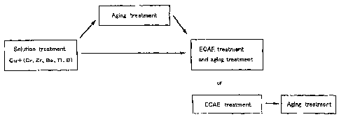
As shown in Figure 1, first Cr is caused to melt into a base material (Cu) in
an
amount of 0.1 to 1.4 wt% and a material in which Cr dissolves in Cr in a solid
CA 02492925 2005-O1-18
- 11 -
solution state in a supersaturated manner is obtained by quenching the spelt.
Subsequently, a strain equivalent to an elongation of not less than 200% is
applied to
this material. Incidentally, it is de$irable to use a material that is
subjected to aging
treatment after solution treatment.
When an added element is Zr, the Zn content is 0.15 to 0.5 wt%. In the case
of Be, the Be content is 0.1 to 3.0 wt%. In the case of Ti, the Ti content is
0.1 to 6.0
w~/°. And in the case of B, the B content is 0.01 to 0.5 wt%.
Figure 2 shows a die that applies a strain by use of a Cu tube. The
above-described mixture is filled in the Cu tube and extruded at a die
temperature of
400 to 500°C and an extruding speed of about 1 mm/sec by repeating the
extrusion
four times (ECAE treatment). Thus, a strain is applied to a copper alloy in
which
Cr dissolves in a solid solution state in a supersaturated manner. By this
operation,
the crystal grain size decreases to pat more than 20 ~n from 200 N.m.
If de: amount of strain, ~: 1/2 of inner angle of joint, ERR: area ratio
before
and after working, A0: sectional area before working, A: sectional area after
working,
EAR: reduction ratio of equivalent sectional area before and after working,
EE:
equivalent strain (elongation), then the following relationships hold:
~e = 2/~3cotanyr
E1ZR = AO/A = exp (de)
EAR = (1 -1/ERR) x 100
EE = (ERR -1 ) x 100
The crystal stzucture becomes grain-refined by the above-described lateral
extrusion (ECAE treatment). Because extrusion conditions overlap aging
treatment,
the precipitation of a second element is promoted at the same time with gram
refinement.
The crystal structure of a copper alloy obtained by this ECAE treatment is
shown in a microgtaph of Figure 3(a). The crystal structure before ECAE
treatment
CA 02492925 2005-O1-18
- 12 -
is shown in a micrograph of Figure 3(b). From these microgaphs, it is apparent
that an added element has precipitated (black points in the photograph) among
crystal gains due to the ECAE treatment.
Figure 4 is a graph that shows the relationship between die temperature and
hardness, Figure 5 is a gaph that shows the relationship between die
temperature and
electrical conductivity, and Figure 6 is a graph that shows the relationship
between
die temperature and thermal conductivity. Fmm these graphs it is apparent that
a
copper alloy related to the Invention has properties required of an electrode
material
such as a welding tip, i.e., a hardness of not less than 30 HRB; an electrical
conductivity of not less than 85 IACS%, and a thermal conductivity of not less
than
354 'W/(m-K).
That is, from Figures 4 to 6, it is apparent that a material not subjected to
ECAE treatment (solution hutment + aging treatment) is inferior in electrical
conductivity and fihenm~al conductivity although it has high hardness, that a
material
obtained by subjecting a material which has been subjected to only the
solution
treatment to ECAE treatment is excellent in electrical conductivity and
thermal
conductivity although it has low hardness, and that a material obtained by
subjecting
a material which has been subjected to aging treatment after solution
treatment to
ECAE treatment is excellent in all respects of hardness, electrical
conductivity and
thermal conductivity.
Figure 7 is a graph that compares the weldability of a copper alloy obtained
by a manufacturing method related to the invention with that of conventional
copper
alloys in terms of the occurrence of spatters and weld sticking. The copper
alloy
related to the invention is equivalent to the alumina-dispersed copper and the
copper
alloy before aging treatment in terms of appzopriate current conditions, and
weld
sticking does not occur.
CA 02492925 2005-O1-18
- 13 -
Figure 8 is a graph that compares the weldability of a copper alloy obtained
by a manufacturing method related to the invention with that of conventional
copper
alloys in terms of the number of welds in continuous spot welding. When the
copper alloy related to the invention was used as a welding tip, it was
possible to
produce 1475 welds in continuous spot welding.
As described above, a copper allay related to the invention has a fine crystal
structure attd a large amount of added element precipitates among crystal
grains and,
therefore, it is possible to ensure that a copper alloy related to the
invention
simultaneously provides mechanical strength and thermal and electrical
properties
that have hitherto been in a tradeoff relation.
Ia particular, it is possible to obtain a copper alloy that has the properties
reduired of an electrode material such as a welding tip, concretely, a
hardness of not
less than 30 HRB, an electrical conductivity of not less than 85 IACS%, and a
thermal conductivity of not less than 350 W/(m~K).
Next, titanium (Ti) was selected as an element to be added and copper alloys
were obtained in the same method as described above. Results are shown in
Figures 9 to 12.
Figure 9 is a graph that shows the relationship between the amount of added
Ti and electrical conductivity. The maximum degree of dissolution of Ti in a
solid
solution state is essentially about 8 wt% and is not vezy large. As shown in
Figure
9, even after aging treatment, about 0.5 wt% of Ti remains in a solid solution
state.
Zt Might be thought that this Ti in a solid solution state lowers the
electrical
conductivity of copper alloys.
Figuze 10 is a graph that shows the electrical conductivity of a copper alloy
that is heavily worked (by application of a strain equivalent to an elongation
of
200%) afker being subjected to aging treatment at 470°C for twa hours
and the
electrical wnductivity of a copper alloy subjected to only aging treatment.
From
CA 02492925 2005-O1-18
- 14 -
this graph it is apparent that the electrical conductivity of the heavily
worked copper
alloy increases greatly. It might be thought that this is because the Ti in a
solid
solution state precipitates due to heavy working.
Figure 11 is a graph that compares the hardness of a heavily worked coppet
alloy with that of a copper alloy subjected to only aging treatment. As shown
in
this graph, the hardness of the heavily worked copper alloy is lower than that
of the
copper alloy subjected to only aging treat~tnent. It might be thought that the
Ti that
has contributed to solid solution strengthening precipitates due to heavy
working.
Figure 12 is a graph that shows the relationship among hardness, electrical
conductivity and heavy working temperature. From this graph it is apparent
that a
Cu-Ti alloy is inferior in electrical conductivity and that electrical
conductivity
Increases although hardness decreases with increasing heavy working
temperature.
Also in this case, it might be thought that the Ti that has contributed to
solid solution
strengthening precipitates due to heavy working.
Thus, by combining heavy working with aging treatment, it becomes possible
to cause the Ti that dissolves in a solid solution state to precipitate from
the copper
matrix although it has hitherto been impossible to cause this Ti to
precipitate by
aging treatment. In addition, the amount of Ti that precipitates can be
controlled by
controlling the degree of heavy working. Therefore, it is possible to make a
copper
alloy having properties that suit the purpose.
Next, boron (B) wss selected as an element to be added, and copper alloys
were made by Various methods. The zelationship between the boron (TiB) of the
obtained copper alloys and electrical conductivity is shown in Figure 13. As
methods of obtaining the copper alloys, [1J preparation of a refined material
subjected to solution treatment, [2] addition of a TiBa powder as a compound
(ceramic) to copper, and [3J a method of adding a Ti powder and a B powder
independently to copper were adopted.
CA 02492925 2005-O1-18
- 15 -
From Figure 13, it became apparent that in all cases electrical conductivity
decreases with increasing addition ratio of TiB and that in terms of
manufacturing
methods, the highest electrical conductivity is obtained 1n the case of a
refined
material although electzical conductivity increases by performing heavy
working.
Figures I4 to 16 explain another embodiment (a composite copper material).
First, as shown in Figure 14, an alumina (A1203) powder or a titanium boride
(TiEZ)
is mixed with a base material (a Cu powder). The mixing proportion is 0.1 wt%
to
~.0 wt%. rf the mixing proportion is less than 0.1 wt%, wear resistance is not
improved. If the mixing proportion exceeds 5.0 wt%, electrical conductivity
decreases and die life also shortens. Therefore, the above-described range is
specified.
Subsequently, the above-described mixed powder is formed into a primary
shaped body in order to perform lateral extrusion. A primary shaped body is
formed, for example, by green compacting or by filling the mixed powder in a
Cu
(copper) tube. Subsequently, a strain equivalent to not less than 200%,
preferably,
about 220% is applied to the primary skiaped body by lateral extrusion.
Incident811y, in Figure 14, for the sake of easy understanding, the diameter
of
the Cu tube is larger than the diameter of an insertion hole formed in the
die. In
actuality, however, the diameter of the Cu tube is almost the same as the
diameter of
the insertion hole formed in the die. The Cu tube is supported with a jig or
the Iike
so that the Cu tube does riot fall while the Cu tube is being pushed in by use
of a
punch.
Concrete conditions for the lateral extrusion are such that the die
temperature,
is 400 to 1000°C and the extrusion speed is about 1 mm/sec, and ECAE
treatment is
performed by repeating extrusion 12 times under the conditions. Ey repeating
the
extrusion, the parent phase becomes grain-ref~.ned and the crushing and
dispersion of
the cexarnic occur.
CA 02492925 2005-O1-18
- m -
The micrographs of crystal structures of the copper alloys obtained by this
ECAE treatment are shown in Figures 15(a) and 15(b). Figure 15(a) shows a
composite material to which an alumi.na. powder is added, and Figure 15(b)
shows a
composite material to which a titanium boride powder is added. From these
photographs, it is ascertained that alumina or titanium boride having a
particle size of
several manometers is unifomtly dispersed in the copper mattix.
Figure 16 is a graph that compares the weldability of composite copper
materials obtained by a manufacturing method related to the invention with
that of a
conventional composite copper material in terms of the number of welds in
continuous spot welding. The number of welds in continuous spot welding is
about
1200 when a commercially available composite copper material izt which alumina
is
dispersed in copper is used as a welding tip, whereas the number of welds in
continuous spot welding is about 1600 in the case of an alumina-dispersed
composite
rapper material subjected to ECAE (equal-channel-angular-extrusion) treatment
and
1900 welds in continuous spot welding were possible when a composite copper
material related to the invention is which titanium boride is dispersed was
used as a
welding tip.
Because solution treatment is not a starting point in this embodiment, there
is
no restriction by the limit of dissolution in a solid solution state and it is
possible to
arbitrarily set the proportion of the particles of a second element (A1203 or
TiB2) in a
copper ahoy. Therefore, it is possible to obtain properties that could not be
obtained in conventional composite copper materials.
That is, the purity of the matrix of a copper alloy is high, a copper alloy is
excellent in electrical properties, and the particle size of particles of
A1z03 or TiB2
that precipitate at the interfaces of matrix particles is on the order of
manometers (not
more than 500 nm) because of the suppression of grain growth. Also, the amount
to
be added can be arbitrarily set.
CA 02492925 2005-O1-18
- 1~
Next, a description will be given of an embodiment in which as a starting
material, a titanium (Ti) powder and a boron (B) powder are mixed with the
base
material (Cu powder).
Figure 17 is a drawing to explain the processes for obtaining a composite
copper material related to the ernbodimeut, in both of which the mixing
proportion of
both the titanium powder and the boron powder in the starting material is 0.1
wt% to
5.0 wt%, If the mixing proportion is less than 0.1 wt%, wear resistance is not
improved. If the mixing proportion exceeds 5.0 wt%, elec~ical conductivity
deczeases and die life also shortens. Therefore, the above-described range is
specified.
Subsequently, the above-described mixed powder is formed into a primary
shaped body in order to perform lateral extrusion. There are available two
processes for obtaining a primary shaped body. When a product to be produced
is a
small one like a connector and an electrode rod, the above-described mixture
is filled
in the Cu tube to form a pximary shaped body. On the other hand, when a
product
to be produced is a long one or a large-sized one, a primary shaped body is
formed
by green compacting.
Subsequently, the above-described primary shaped body is sintered. The
added titanium (Ti) and boron (B) react due to the thermal energy resulting
from this
sintering to foam titanium boride. Figure 18 shows the condition of a
structure after
sintering. From this figure it is apparent that the titanium boride not formed
before
sintering is formed.in the copper matrix after sintering.
Incidentally, although sintering was perfarmed as means for applying thermal
energy in the embodiment, thermal energy may be applied by means other than
this.
A strain equivalent to not less than 200%, preferably not less than about 220%
is applied to the primary shaped body after sintezing thus obtained by lateral
CA 02492925 2005-O1-18
- 1~ -
extrusion. The lateral extrusion is performed by the same method as described
above.
Concrete conditions for the lateral ex~usion are such that the material
temperature is 400 to 1000°C, the die temperature is 400 to
500°C and the extrusion
speed is about 1 mm/sec, and ECAE (equal-channel-angular-extrusion) treatment
is
performed by repeating extrusion 12 times under the conditions. By repeating
the
operation, the parent phase becomes grain-refined and the crushing and
dispersion of
the titanium boride formed in the copper matrix occur.
Figure 19 is a drawing that shows the relationship between electrical
conductivity and amount of added TiB when heavy working (applying a strain
equivalent to an elongation of 220%) is performed and when heavy working is
not
perfornned. From this figure it became apparent that ekectrical conductivity
is
increased by heavy working. Although titanium boride having electrical
conductivity is formed by the above-described heat treatment, electrical
conductivity
cannot be increased. It is not that the added titanium and boron react
stoichiometrically, but that the added titanium and boron in a solid solution
state
remain within the copper matrix while they are still unreacted. Therefore, it
might
be thought that the unreacted solute elements (titanium and boron) precipitate
when
heavy working is performed, with the result that electrical conductivity
increases.
.Also for complex copper materials related to the invention, wekdability was
verified by the number of welds in continuous spot welding and the same
results as
shown in F baurc 16 were abtained_
Because solution treatment is not a starting point in a method of
manufacturing a composite copper material rekated to this embodiment, there is
no
restriction by the limit of dissolution in a solid solution state, and it is
possible to
arbitrarily set titanium and boron to be added to copper, and it is possible
to obtain
properties that could not be obtained in conventional composite copper
materials.
CA 02492925 2005-O1-18
- 19 -
In particular, because titanium boride is not directly added to copper and
because titanium and boron before the reaction arc added to cause titanium
boride to
be formed in the copper matrix by tlxe reaction by applying thermal energy to
the
titanium and boron before the reaction, the grain refinement of a structure
(in the
order of nanometers: not more than hundreds of nanometers) is promoted and
mechanical strength increases.
Industrial Applicability
A copper alloy and a composite copper material related to the invention can
be used as a material for a connector that constitutes part of wiring of
electric
vehicles and the like or a material for welding electrodes.