Note : Les descriptions sont présentées dans la langue officielle dans laquelle elles ont été soumises.
CA 02494125 2010-12-06
1
"SUPERCONDUCTING QUANTUM INTERFERENCE DEVICE"
Technical Field
The present invention relates to superconducting devices having
elements positioned in three dimensions, and in particular to high temperature
superconducting devices having elements positioned in three dimensions. The
invention particularly relates to high temperature superconducting axial
gradiometers, which employ a gradiometric pick-up loop formed by etching a
transformer loop structure on a flexible superconducting tape. The pick-up
loop
is preferably inductively coupled to a superconducting quantum interference
device (SQUID) magnetometer. In applications where the sensitivity to the
magnetic field in the direction transverse to the gradiometer axis is
problematic,
the homogeneous background magnetic field can be reduced by matching the
mutual inductance between the secondary loop of the flux transformer and the
magnetometer to establish a condition of shielding.
Background Art
Superconducting Quantum Interference Devices (SQUIDs) are often
used as highly sensitive magnetic field sensors. Such SQUID sensors are
becoming increasingly popular due to the capabilities of high sensitivity
sensing
in areas such as geophysical mineral prospecting and biological magnetic field
detection, such as magnetic field emanations from the human brain or other
human organs.
With the advent of high critical temperature superconducting (HTS)
materials such as YBa2Cu30õ (YBCO), HTS-SQUIDs can operate at or above
77K (-196 C) and hence can be cooled by relatively inexpensive liquid
nitrogen,
rather than requiring liquid helium as a coolant for operation at 4K (-269 C).
Liquid nitrogen is also more convenient to use than liquid helium, allowing
the
system as a whole to be made in a compact form.
The use of high-temperature superconducting (HTS) materials for the
fabrication of SQUID based magnetometers and gradiometers is now fairly well
established (For example, W. Eidelloth, B. Oh, R. P. Robertazzi, W. J.
Gallagher, R. H. Koch, Appl. Phys. Lett., 59, 3473 (1991); S. Knappe, D.
Drung, T. Schurig, H. Koch, M. Klinger, J. Hinker, Cryogenics 32, 881, (1992);
M. N. Keene, S. W. Goodyear, N. G. Chew, R. G. Humphreys, J. S. Satchell, J.
A. Edwards, K. Lander, Appl. Phys. Lett. 64, 366 (1994); G. M. Daalmans,
CA 02494125 2010-12-06
2
Appl. Supercond. 3, 399, (1995); M. I. Faley, U. Poppe, K. Urban, H.-J.
Krause,
H. Soltner, R. Hohmann, D. Lomparski, R. Kutzner, R. Wordenweber, H.
Bousack, A. I. Braginski, V. Y. Slobodchikov, A. V. Gapelyuk, V. V. Khanin,
Y.V. Maslennikov, IEEE Trans. Appl. Supercond., 7, 3702 (1997)). Despite the
significant advantages which accrue from being able to operate at liquid
nitrogen temperatures, HTS materials remain more difficult to use than the
alternative low-temperature superconducting materials, and many design
practices in low temperature helium cooled superconductors (LTS) cannot be
implemented in HTS materials. In particular, the lack of HTS superconducting
wires and the difficulty of forming superconducting connections in HTS
materials means that the standard LTS design practice of forming gradiometer
coils from superconducting wires, is not applicable in HTS materials.
Designs for HTS gradiometers sensitive to the on-diagonal components,
aBliaXi (axial gradiometers), have been described (for example: R. H. Koch,
J. R. Rozen, J. Z. Sun, W. J. Gallagher, Appl. Phys. Lett., 63, 403,(1993); H.
J.
M. ter Brake, N. Janssen, J. Flokstra, D. Veldehuis, H. Rogalla, IEEE Trans.
Appl. Supercond., 7, 2545, (1997); J. Borgmann, P. David, G. Ockenfuss, R.
Otto, J. Schubert, W. Zander, A.J. Braginski, Rev. Sci. lnstrum. 68,
2730,(1997)
but these have been implemented only by means of electronic or software
subtraction of the outputs of a pair of SQUID magnetometers which are
generally positioned at fixed distances from each other on a common normal
axis. These designs suffer from the disadvantage that both magnetometers
must operate linearly in the full ambient field (often the earth's magnetic
field). It
is difficult to achieve good common-mode rejection (rejection of homogeneous
fields) which is generally limited to an order of about 1.0-3
in most
implementations. Furthermore, the achievable noise performance can be
dependent upon the magnitude of the background homogeneous field; being
determined by microphonics which arise from vibrations causing randomly
varying misalignment of the axes of symmetry of the two SQUIDs.
Some of these problems are ameliorated by the use of intrinsic gradiometer
structures. Although several designs for intrinsic magnetic gradiometers
utilising HTS films have been described in the literature these designs are
CA 02494125 2010-12-06
_
3
sensitive only to the off-diagonal components of the first-order gradient
tensor,
aBi/aXi , i i
- = ..) (transverse gradiometers). These designs generally fall into
one of two types. The first employs a "figure eight" topology in which the
gradiometric pick-up loop structure consists of a pair of superconducting
loops
with a common conductor that is interrupted by a direct current (DC) SQUID.
The SQUID operates as a two-port device (SQUID amplifier) because the flux
in the SQUID is derived from the current directly injected into a pair of
input
terminals. Depending upon the matching of the inductances and equivalent
magnetic areas of the gradiometer input loops the current in the SQUID is
proportional to the difference in the shielding currents induced in the pick-
up
loops in response to an external magnetic field gradient. The two pick-up
loops
are electrically in parallel, so one disadvantage of this topology is that
even in a
homogeneous field a large overall shielding current is induced in the outer
perimeter of the pick-up loop structure with the potential to degrade noise
performance through the associated production of large numbers of Abrikosov
vortices in the superconducting film.
Another approach to the development of HTS transverse gradiometers
employs a planar pick-up loop structure that is flip-chipped with a SQUID
magnetometer to which it is inductively coupled. In the first-order designs
the
flux transformer consists of a pair of pick-up loops, one of which is coupled
to
the SQUID magnetometer. By matching the mutual inductance between the
SQUID and the loop, the total effective magnetic area of the SQUID/loop
combination can be made exactly opposite to that of the other loop of the flux
transformer. Under these conditions the sensitivity to a homogeneous magnetic
field vanishes but remains non-zero with respect to a magnetic field gradient.
A
second-order transverse gradiometer has also been implemented using this
approach.
Any discussion of documents, acts, materials, devices, articles or the like
which has been included in the present specification is solely for the purpose
of
providing a context for the present invention. It is not to be taken as an
admission that any or all of these matters form part of the prior art base or
were
common general knowledge in the field relevant to the present invention as it
existed before the priority date of each claim of this application.
Throughout this specification the word "comprise", or variations such as
"comprises" or "comprising", will be understood to imply the inclusion of a
CA 02494125 2012-02-24
_
4
stated element, integer or step, or group of elements, integers or steps, but
not the
exclusion of any other element, integer or step, or group of elements,
integers or
steps.
Throughout this specification, the terms 'superconducting material',
'superconducting device' and the like are used to refer to a material or
device
which, in a certain state and at a certain temperature, is capable of
exhibiting
superconductivity. The use of such terms does not imply that the material or
device
exhibits superconductivity in all states or at all temperatures.
Summary of the Invention
Certain exemplary embodiments can provide a superconducting magnetic
field detection element comprising at least one superconducting pick-up loop
formed on a common flexible substrate, wherein the common flexible substrate
is in
a non-planar position, such that the at least one superconducting pick-up loop
is
operable to detect magnetic fields of differing orientation, and further
comprising a
flux transformer configured for inductive coupling of detected signals to a
superconducting quantum interference device (SQUID).
Certain exemplary embodiments can provide a superconducting magnetic
field detection element comprising a plurality of superconducting pick-up
loops
formed on a common flexible substrate, wherein the common flexible substrate
is in
a non-planar position, such that the plurality of superconducting pick-up
loops are
operable to detect magnetic fields of differing orientation, and further
comprising a
flux transformer configured for inductive coupling of detected signals to a
superconducting quantum interference device (SQUID).
Certain exemplary embodiments can provide a method of forming an
element of a superconducting device for detecting magnetic fields, the method
comprising: forming at least one superconducting pick-up loop on a common
flexible substrate, and forming a flux transformer on the common flexible
substrate
for inductive coupling of detected signals to a superconducting quantum
interference device (SQUID); and positioning the common flexible substrate in
a
non-planar configuration such that the at least one superconducting pick-up
loop is
operable to detect magnetic fields of differing orientation.
CA 02494125 2012-02-24
4a
Certain exemplary embodiments can provide a method of forming an element of
a superconducting device for detecting magnetic fields, the method comprising
the
steps of: forming a plurality of superconducting pick-up loops on a common
flexible
substrate, and forming a flux transformer on the common flexible substrate for
inductive coupling of detected signals to a superconducting quantum
interference
device (SQUID); and positioning the common flexible substrate in a non-planar
configuration such that the plurality of superconducting pick-up loops are
operable to
detect magnetic fields of differing orientation.
In some embodiments of the invention, the common flexible substrate may
partially extend within a first plane and partially extend within a second
plane
substantially perpendicular to the first plane such that the at least one
superconducting
pick up loop is positioned in both the first plane and the second plane. Such
embodiments of the invention may prove advantageous when a magnetic dipole of
unknown random orientation is placed at a position where a normal to the first
plane
meets a normal to the second plane. The positioning of the at least one pick-
up loop
in two perpendicular planes increases the likelihood that a magnetic field of
the
magnetic dipole will pass through at least some portion of the pick-up loop,
and will
thus induce a current in the pick-up loop, enabling detection of the magnetic
dipole.
CA 02494125 2010-12-06
Alternatively, the common flexible substrate may be positioned such that
the at least one superconducting pick-up loop describes an arc, for example an
arc which subtends an angle of 900 about a nominal focus. In such
embodiments, positioning a randomly oriented magnetic dipole at or near the
5 nominal focus of the arc of the pick-up loop will provide a higher
likelihood of
detecting the magnetic dipole than would exist in cases where the pick up loop
is positioned within a single plane. Such embodiments of the present invention
may have particular application in the screening of substances or articles for
detection of randomly oriented embedded magnetic objects.
In further embodiments of the present invention, a plurality of
superconducting pick up loops may be formed on the common flexible
substrate. In such embodiments the common flexible substrate may be
arranged so as to position each of the plurality of pick up loops in a unique
plane which is not coplanar with any plane in which another pick up loop is
positioned. For example, two superconducting pick up loops may be provided,
and may be positioned in respective first and second planes, the first and
second planes being substantially perpendicular to each other. Alternatively,
two superconducting pick up loops may be provided and may be positioned in
respective first and second planes, the respective first and second planes
being
parallel to each other and spaced apart.
Further, in embodiments of the invention in which a device is provided
having two superconducting pick-up loops formed on the common flexible
substrate, the inherent characteristics of the two superconducting pick-up
loops, such as critical current and effective area, are likely to be
significantly
closer to being matched than would be the case for the characteristics of pick-
up loops or devices formed on separate substrates. Thus, the error margin of
such devices can be expected to be significantly smaller, and indeed, magnetic
fields of up to 108 lower than the earth's magnetic field may be detected by
some embodiments of the present invention. Additionally, embodiments of the
present invention which provide two superconducting pick-up loops on the
common flexible substrate enable construction of magnetic field detection
devices such as axial gradiometers which comprise only a single SQUID. Such
circuits offer significant advantages over circuits requiring the extra
complexity
of providing a plurality of SQUIDs, in terms of both physical device
manufacture
and the device electrical characteristics.
CA 02494125 2013-03-27
6
Superconducting tape has been developed primarily for power transmission
applications. In early developments such tape was formed using powder in
silver
tube filled with one of the various ceramic HTS materials but more recently
developments in tape technology have led to the ability to form YBCO films on
both
metal and insulating substrates with an intervening buffer layer.
In preferred embodiments of the present invention, the common flexible
substrate may comprise Hastelloye tape, preferably of 50 to 200 rn thickness.
In
addition to providing a common flexible substrate in accordance with the
present
invention, Hastelloy tape is also advantageous in that a pick-up loop of
significantly
larger area may be formed at significantly less cost, when compared to non-
flexible
crystalline substrates such as MgO, SrTiO3, LaA1203 or the like. In alternate
embodiments of the present invention, the common flexible substrate may
comprise
a partially or fully stabilised zirconia substrate, for example in very thin
flexible sheet
form, such as is provided under the name CeraflexTM by MarkeTech International
of
4750 Magnolia St, Port Townsend, WA, 98368, USA. Cerafleirm has been found to
possess improved noise properties over Hastelloy tape, enabling an SNR of a
superconducting device formed over the CeraflexTM substrate to be improved by
perhaps 30% relative to Hastelloye tape.
In embodiments of the present invention in which the common flexible
substrate is a polycrystalline substrate such as Hastelloy or CeraflexTM, a
biaxially aligned buffer layer such as yttria-stabilised zirconia (YSZ) is
preferably
formed over the common flexible substrate in order to improve biaxial
alignment of a superconducting material from which the at least one
superconducting pick up loop is formed. The buffer layer may be deposited by
ion
beam assisted deposition (IBAD), or by double ion beam assisted deposition
(DIBAD), as set out in the present applicant's co-pending International Patent
Application No. PCT/AU02/00696.
In embodiments of the present invention, a magnetic field passing through
the at least one pick up loop which induces a current in the at least one
pick up loop may be detected by use of a SQUID. The SQUID may be
formed on the common flexible substrate. Alternatively the SQUID may be
magnetically coupled to the at least one pick up loop by way of a flux
transformer
formed on the common flexible substrate, and by positioning the
CA 02494125 2010-12-06
7
SQUID to allow coupling between the flux transformer and the SQUID. For
example the SQUID may be mounted against the flux transformer in a "flip-
chip" arrangement.
The present inventors have recognised that it is possible to use flexible
substrates, such as HasteHoy tapes or CeraflexTM, to support a biaxially
aligned buffer layer and thus to support a flexible superconducting circuit,
formed over the buffer layer. For instance, such substrates may be used to
support flexible superconducting circuits such as large area pick-up loops for
magnetometers. Thus, the present invention extends the applications of
superconducting tape utilising such flexible substrates to include use as a
flexible superconducting medium for the fabrication of flexible
superconducting
circuits including gradiometer pick-up loops and flexible ground-planes for
superconducting strip-lines. Further such applications include the formation
of
flexible superconducting wave-guides. In many such applications envisaged by
the present invention, even relatively short lengths of tape, of the order of
a few
hundred millimeters, would be sufficient.
Accordingly, in a third aspect, the present invention provides a flexible
superconducting device comprising a flexible polycrystailline substrate, a
biaxially aligned buffer layer, and at least one superconducting component
formed over the biaxially aligned buffer layer.
Similarly, according to a fourth aspect the present invention provides a
method of forming a flexible superconducting device, the method comprising:
providing a flexible polycrystalline substrate;
forming a biaxially aligned buffer layer over the flexible polycrystalline
substrate; and
forming at least one superconducting component over the biaxially
aligned buffer layer.
In accordance with embodiments of the third and fourth aspects of the
present invention, the flexible superconducting device may comprise one or
more of the following non-limiting list of superconducting devices: a pick up
loop; a ground plane; a strip-line connector; a waveguide, a flux transformer;
a
Josephson Junction; and, a SQUID.
A smallest radius of curvature of the common flexible substrate should
be controlled. This is due to the possibility of an overly tight curvature of
the
device causing damage to the polycrystalline flexible substrate, the biaxially
aligned buffer layer, the crystalline superconducting layer or any other layer
CA 02494125 2010-12-06
8
such as an overlying silver passivating layer. Depending on the materials from
which the common flexible substrate, the buffer layer, the superconducting
pick
up loops, and any other layers such as a passivation layer are formed, the
minimum permissible radius of curvature of the device may vary.
The tape may also be twisted in order to provide circuit elements in a
third plane, for example, to provide elements in three orthogonal planes. Once
again, a minimum radius of curvature or twist is preferably controlled in
order to
avoid damage to the device.
According to a fifth aspect, the present invention provides a
superconducting gradiometer comprising:
a first pick-up loop defining and substantially residing in a first nominal
plane; and
a second pick-up loop defining and substantially residing in a second
nominal plane;
wherein the first pick-up loop and the second pick-up loop are formed on
a common flexible substrate, wherein the first nominal plane and the second
nominal plane are substantially parallel, and wherein the first nominal plane
and the second nominal plane are sufficiently spaced apart to allow the first
pick-up loop and the second pick-up loop to act to distinguish local magnetic
fields from background magnetic fields.
By providing first and second pick-up loops which are formed on a
common flexible substrate, the fifth aspect of the present invention allows a
gradiometer to be constructed without the need for separately formed
connections between the first pick-up loop and the second pick-up loop.
The use of a flexible substrate in accordance with the fifth aspect of the
present invention allows formation of the superconducting gradiometer in a
single plane, such as by planar deposition techniques. After the pick-up loops
have been formed on the flexible substrate, deformation or bending of the
flexible substrate allows the first and second pick-up loops to be
respectively
positioned in the first and second nominal planes.
Positioning the first and second pick-up loops in accordance with the fifth
aspect of the invention enables construction of a superconducting axial
gradiometer. In some embodiments of the fifth aspect of the present invention,
such an axial gradiometer may be implemented through the use of a
superconducting flux transformer pick-up loop structure patterned on the
CA 02494125 2010-12-06
9
common flexible substrate, the flux transformer pick-up loop being inductively
coupled to a SQUID magnetometer.
In such embodiments, the axial gradiometer includes a flux transformer
that is formed by patterning an appropriate circuit using conventional resist
techniques over the superconducting layer of the tape, which for instance may
be a YBCO layer formed over a biaxially aligned buffer layer of the flexible
substrate. In such embodiments, the flux transformer comprises two outer
pick-up loops which are connected in series with a centrally located secondary
loop via a pair of flexible strip-line conductors. A SQUID magnetometer is
then
"flip-chipped" over the secondary loop and separated from the secondary loop
by means of insulating spacers. In such embodiments, two additional lengths
of flexible superconducting tape are preferably used to cover the strip-line
connectors between each outer pick up loop and the secondary loop. With
respect to the strip-line connectors, the additional lengths of flexible
superconducting tape form a ground-plane. These additional lengths of flexible
superconducting tape are preferably configured so as to serve three purposes.
Firstly, such additional lengths of superconducting tape may serve to reduce
unwanted shielding currents which might otherwise be induced in the loop
structure from the strip-line connectors, and secondly may serve to reduce the
inductance of the strip-line connectors. The effect of the strip-line
inductance
on the performance of the gradiometer is considered in more detail below.
Finally, the additional superconducting tape ground-planes may, if necessary,
be used to facilitate balancing or matching of the equivalent areas of the
primary pick-up loops, for instance by sliding the additional superconducting
covering ground tapes so as to expose an appropriate area of strip-line to the
external field in a manner which balances the equivalent areas of the two
outer
pick up loops.
In preferred embodiments of the present invention, the flexible substrate
comprises a flexible tape made of a rolled metal alloy such as Hastelloy .
Advantageously, a CeraflexTM tape may alternatively be used. In the past,
CeraflexTM tapes have not been used for HTS applications, however it has
been realised by the present inventors that CeraflexTM tape provides improved
noise performance over traditional tapes such as Hastelloy tape, improving
the SNR of a superconducting device formed on the tape by perhaps 30%
relative to Hastelloy tape.
CA 02494125 2010-12-06
A buffer layer may be positioned between the substrate and the pick-up
loops, for example to promote biaxial crystal alignment in superconducting
material from which the pick-up loops are formed, and/or to isolate the
superconducting material from the substrate. The buffer layer may comprise a
5 biaxially aligned yttria-stabilised zirconia (YSZ) layer. The
superconducting
material may be YBa2Cu307 (abbreviated as YBCO) or Bi1.6Pb0.4Sr2Ca2Cu3Olo
(abbreviated as BSCCO). A protective layer such as an Ag layer can be
provided over the superconducting material from which the pick-up loops are
formed.
10 In preferred embodiments of the fifth aspect of the invention, a flux
transformer is provided between the first and second pick-up loops in order to
couple detected flux into a SQUID proximal to the flux transformer. For
example, a SQUID may be formed by conventional means on a separate
substrate and "sandwich-mounted" against the flux transformer, in a "flip-
chip"
arrangement as described previously.
Alternatively, a SQUID may be formed on the flexible substrate itself, by
formation of a Josephson Junction, for example over a step edge etched into
the substrate.
According to a sixth aspect, the present invention provides a method of
fabrication of a superconducting gradiometer comprising the steps of:
forming a first pick-up loop and a second pick-up loop on a flexible
substrate positioned substantially in a single nominal plane; and
subsequently deforming the flexible substrate to position the first pick up
loop substantially in a first nominal plane and to position the second pick-up
loop substantially in a second nominal plane, wherein the first nominal plane
and the second nominal plane are substantially parallel and are spaced
sufficiently apart to allow the first pick-up loop and the second pick-up loop
to
act to distinguish local magnetic fields from background magnetic fields.
The method of the sixth aspect of the invention may comprise the
additional steps of:
forming a flux transformer on said flexible substrate; and
sandwich mounting a SQUID against the flux transformer.
It will be appreciated that the step of forming a flux transformer may be
most conveniently carried out simultaneously with the step of forming said
first
and second pick-up loops.
CA 02494125 2010-12-06
11
Alternatively, the method of the sixth aspect of the invention may
comprise the additional steps of:
forming a step edge on the flexible substrate; and
forming a SQUID on the flexible substrate, having a Josephson Junction
formed over said step edge.
The method of the sixth aspect of the invention may comprise the
additional steps of:
forming a buffer layer over the flexible substrate prior to formation of said
pick-up loops; and/or
forming a protective coating over the first and second pick-up loops.
The buffer layer may be biaxially aligned YSZ, and may serve to promote
biaxial growth of superconducting material from which the pick-up loops are
formed, and may serve to isolate the pick-up loops from the substrate. The
protective coating may be a silver coating.
To date, HTS flexible tapes have mainly been considered for power
transmission purposes. Thus, it is envisaged that a relatively thin
superconducting layer of perhaps 50-500 nm may be used in the present
invention, as opposed to thicker power-carrying superconducting layers.
Brief Description of the Drawings
By way of example only, preferred embodiments of the invention will be
described with reference to the accompanying drawings, in which:
Figure 1 illustrates a HTS gradiometer in accordance with a first
embodiment of the present invention;
Figure 2 illustrates a magnetic field detection element in accordance with
a second embodiment of the present invention;
Figure 3 illustrates a magnetic field detection element in accordance with
a third embodiment of the present invention;
Figures 4(a) to 4(c) illustrates a HTS gradiometer in accordance with a
fourth embodiment of the present invention;
Figure 5 illustrates the variation of the magnetometer current and
gradient sensitivity with a stripline inductance of 20 nH;
Figure 6 illustrates the variation of the magnetometer current and
gradient sensitivity with a stripline inductance of 5 nH and
Figure 7 illustrates the variation of the magnetometer current and
gradient sensitivity with a stripline inductance of 0.5 nH.
CA 02494125 2010-12-06
12
Description of the Invention
Figure 1 illustrates a high temperature superconducting (HTS) axial
gradiometer 10 in accordance with an embodiment of both the first and fifth
aspects of the present invention. The axial gradiometer comprises a flexible
Hastelloy tape 11, providing a substrate for superconducting elements of the
gradiometer. A buffer layer of YSZ has been grown over a surface of the
Hastelloy tape to enhance biaxial alignment of YBCO formed over the YSZ. A
first pick-up loop 12 formed of YBCO is provided proximal to one end of the
tape 11, and a second pick-up loop 13 also formed of YBCO is provided
proximal to an opposite end of the tape 11. The pick-up loops are connected to
each other via strip-line connectors 14 and flux transformer 15 in a manner
which substantially cancels out common-mode magnetic fields such as the
earth's magnetic field, such that only a magnetic field which has a gradient
between the first and second pick-up loops will cause current to flow in the
superconducting YBCO elements 11, 12, 13, 14, 15.
As can be seen, all superconducting elements of the gradiometer 10 can
be fabricated on a single surface of the tape 11, and can be formed while
positioned in a single plane using planar deposition technologies, see Fig lb.
Further, due to the flexibility of the Hastelloy tape, once fabricated the
first and
second pick-up loops 12, 13 can be axially aligned and positioned in
substantially parallel planes a distance d apart.
A SQUID, not shown, may then be "sandwich mounted" to the Hastelloy
tape 11 so as to be in close proximity to the flux transformer 15 and to
maximise magnetic coupling between the SQUID and the flux transformer 15.
Thus, when current is induced in the flux transformer 15 by a magnetic field
having a gradient between the first and second pick up loops 12, 13, the
current circulating in the flux transformer 15 will induce another magnetic
field,
which will be coupled to the SQUID for detection.
By using only a single SQUID, the present invention enables a HTS
gradiometer to be constructed which does not suffer from the deficiencies
associated with measurements relying on the measurements obtained by two
different SQUIDs having differing inherent characteristics. Further, by using
a
flexible Hastelloy tape or the like, the present invention enables a single
SQUID HIS gradiometer to be constructed, as flexible HIS circuits may be
formed on such a substrate.
CA 02494125 2010-12-06
13
Figure 2 illustrates a magnetic field detection element 20, in accordance
with an embodiment of the first aspect of the present invention. The magnetic
field detection element 20 comprises a first pick up loop 21, a flux
transformer
22, and a second pick up loop 23 not visible but of equal dimensions as pick
up
loop 21. The pick-up loops 21 and 23 and the flux transformer 22 are formed
on a flexible substrate comprising a CeraflexTM tape 25. A buffer layer of YSZ
(not shown) is formed over the tape 25, and the pick-up loops 21, 23 and the
flux transformer 22 are formed of YBCO deposited over the buffer layer.
Tracks 24 connect pick-up loops 21, 23 with flux transformer 22.
In accordance with the present invention, the flexible substrate 25 is
arranged such that the pick-up loop 21 is positioned in a first plane which is
substantially perpendicular to a second plane in which the second pick-up loop
23 is positioned. As indicated at 26, 27, the normals to the planes in which
the
pick-up loops 21, 23 are positioned meet at substantially 90 degrees.
Accordingly, when a magnetic dipole is positioned with random
orientation where the normals 26, 27 meet, the magnetic detection element 20
is more likely to detect the magnetic dipole than prior art arrangements in
which
a pick-up loop is provided in one plane only. For example, if the magnetic
dipole is aligned along axis 27, the field of the dipole will couple strongly
through pick-up loop 23, but will not couple strongly into pick-up loop 21. If
the
magnetic dipole is aligned along axis 26, the field of the dipole will couple
strongly into pick-up loop 21, but will not couple strongly into pick-up loop
23. If
the dipole is aligned at 45 degrees to each axis 26, 27, the field of the
dipole
will couple with equal strength into each pick-up loop.
When a field couples into one or both of pick-up loops 21, 23, current will
be induced. This current will be passed to flux transformer 22, which is
preferably designed so as to maximise magnetic coupling to a SQUID (not
shown) which is to be sandwich mounted onto the tape 25. Detection of the
magnetic field of the dipole can then be carried out with high sensitivity by
the
SQUID.
Figure 3 illustrates a magnetic field detection element 30 in accordance
with another embodiment of the first aspect of the present invention. The
element 30 comprises a first pick-up loop 31, a flux transformer 32 and a
second pick-up loop 33. Pick-up loop 31 subtends an angle 0 of greater than
90 degrees. Consequently, a magnetic dipole aligned along an axis anywhere
within angle 0, will couple relatively strongly through pick-up loop 31.
Similarly,
CA 02494125 2010-12-06
14
a magnetic dipole with an axis which is aligned anywhere within the angle (not
shown) subtended by pick-up loop 33 will couple relatively strongly through
pick-up loop 33. A stronger coupling will induce greater current in the pick-
up
loops 31, 33, and thus provide a stronger signal for detection by a SQUID
sandwich mounted over flux transformer 32.
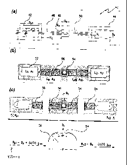
According to a further embodiment there is shown in Figures 4(a) to 4(c)
an HTS gradiometer 40. Figure 4(a) shows a first pick-up loop 42, a second
pick-up loop 44 and a flux transformer 46. Each of the pick-up loops 42, 44
are
directly linked to a secondary loop of the flux transformer 46 via respective
strip
conductors/connectors 48 and 50. Each of the pick-up loops 42, 44 and the
secondary loop of the flux transformer 46 may each be formed of YBCO
material. They are each fabricated on a flexible Hastelloy tape 52, shown in
Figures 4(b) and 4(c) as shading. Figure 4(b shows the gradiometer 40
assembled prior to bending the strip conductor sections 48 and 50. Figure 4(c)
shows a plan and side view of the complete axial gradiometer. A
superconducting ground plane 56 covers each of the strip conductors 48 and
50. In the side view of the gradiometer in Figure 4(c), the ground planes 56
and strip conductors 48, 50 are shown curved with a radius r.
The first pick-up loop 42 has internal dimensions dp1, do and external
dimensions Dp1, Do. The second pick-up loop 44 has similar dimensions to
that of the first pick-up loop 42 and the secondary loop of the flux
transformer
46 has an internal length ds and external length DS. A SQUID may be
sandwich mounted to the Hastelloy tape 52 of which a pick-up loop 54 is
shown which is in close proximity to the secondary loop of the flux
transformer
46 to establish a magnetic coupling therebetween. The magnetometer pick-up
loop 54 has inductance LM and area Am, the secondary loop of the flux
transformer has inductance Ls and effective area As. Each of the pick-up loops
42 and 44 respectively have inductance L1, L2 and equivalent areas Al and A2
respectively.
Shown in Figure 4 (c) is the gradiometer having each of the pick-up
loops 42 and 44 in parallel planes separated by distance d with the stripline
connectors 48, 50 bent with a radial curvature r. Magnetic field Bz is shown
normal to the SQUID and flux transformer 46 whilst the magnetic field
impinging on the first pick-up loop 42 is Bki-Bx+(d/2)gxx and the field
impinging
on the second pick-up loop 44 is Bx2-Bx-(d/2)gxx. Thus when current is
induced in the secondary loop of the flux transformer 46 by magnetic field
CA 02494125 2010-12-06
having a gradient between the first and second pick-up loops 42, 44, the
current circulating in the secondary loop induces a further magnetic field
which
couples with the pick-up loop 54 of the SQUID thereby inducing a further
current which is detected by the SQUID.
5 With regard to the design of the axial grad iometer, the strip-line
sections are
folded to form a "U" shape with the primary pick-up loops aligned on a common
axis that is then perpendicular to the axis of the SQUID. Since the SQUID is
oriented perpendicularly to the gradient pick-up loops, and assuming the
orientation, this device is sensitive to both the first-order axial gradient,
10 aBi/ax, and to the transverse component of the magnetic field B. For
applications in which the sensitivity to Bz must be reduced, this can be
achieved by appropriate design of the secondary loop and SQUID to ensure
shielding of the magnetometer by currents induced in the secondary pick-up
loop. The pick-up loop structure so formed is a series type. This decreases
the
15 magnitude of the shielding current which results from the components of
any
external homogeneous magnetic fields in the plane normal to the SQUID axis.
Currents in the pick-up loops are induced only by a field gradient in the X ¨
direction, mismatches between the magnetic equivalent areas of the primary
loops, direct exposure of the strip-lines to the external field or by
incorrect
mutual inductance between the secondary loop and the SQUID.
The axial grad iometer may also be mounted such that it is possible to rotate
the gradiometer device either the SQUID and pick up loop together or the pick
up loop with the SQUID stationary to achieve further improvements to the
device usefulness. These improvements are:
- true value of the gradient field and magnetic field,
- greatly enhanced common mode rejection of homogeneous fields
- real time information of the condition of the SQUID operation
- if three axial gradiometers are mounted near orthogonally or
orthogonally, jointly they provide all five unique components of the first
order gradient tensor and the three components of the total field
- these improvements can be achieved without the need to attain
perfect
balance usually achieved by the physical alignment of the pick up loops
of the flexible tape.
CA 02494125 2010-12-06
16
Rotation of axial gradiometers of both HTS axial gradiometers described
here and LTS axial gradiometers provides the above enhancements.
Theory of Operation.
Assume a lumped inductance model with all mutual inductances
regarded as negligible other than the mutual inductance, g between the
secondary loop of the flux transformer and the magnetometer. In what follows
it
is assumed that the magnetometer employed is a SQUID based directly-
coupled magnetometer. In this type of magnetometer a superconducting pick-
up loop is used to sense the external magnetic field. The inductance and
equivalent area of the magnetometer pick-up loop will be denoted Lm and Am
respectively. Currents induced in this loop are injected into a SQUID
amplifier
that has a geometry optimized for minimum flux noise. A magnetometer of this
type is assumed for two reasons. Firstly these devices currently provide the
best sensitivity possible from HTSC SQUID based magnetometers, and are
therefore likely candidates for a practical device. Secondarily, as will be
seen
below, the alternative choice of a DC or RF SQUID with a flux-focussing
washer, can be regarded as a special case of the present theory.
Since the magnetometer is coupled to the transformer secondary by a
short-circuit superconducting loop, the flux in this loop is conserved with
respect to changes in the external field. The total flux in the magnetometer
pick-up loop is the sum of the fluxes due to the external field, its own
shielding
current and the flux coupled via the mutual inductance "from the current 13 in
the secondary loop of the transformer. Assuming, without loss of generality,
that the device is zero field cooled (Z.F.C), this sum vanishes, i.e.
BzAm ¨ ImLm ¨ Aff = 0
The flux transformer is also a shorted superconducting loop, so once
again assuming it is Z.F.0
BA-2A2 ¨ BxiA 1 ¨ IL -h BA, ¨ LW = 0
where Lis the total inductance of the transformer, i.e.:
L = L1 -I- L 2 -h 2Lc -h Ls.
CA 02494125 2010-12-06
17
Lk, Akdenote the inductance and equivalent area of the primary loop k,
(k = 1,2), L1n the inductance of each of the strip-lines and LsiSthe
inductance of the secondary loop.
Solving equations and simultaneously gives for the magnetometer current
dMAgõ,, ¨ Bz[AmL ¨ MAs]
Im ¨
M2 ¨ L L
m
where Ai = A27-5.-- A5and
Bx2 ¨B1 =2 xx
(Bx -h d2 gxx) ¨ (Bx ¨ d6 cr )
= dg
,,xx
This can be re-written in terms of the coupling constant aby use of the
standard relation
M= a ,,ILmL,
to yield
L
Bz(Amt-71 ¨ ails .1--1--s )¨ a gxxI
dA ,
Lin ¨ A Lin
I,õ = _____________________________________________________
2(Lp + Lc) + L,(1 ¨ a2)
where L1 = L2 --7-A8' LP =
Condition for shielding to suppress sensitivity to B.
= :
If the external field is homogeneous gxx = and equation becomes
L ¨ aA Ls
'm Lm s il Ln2
1 pfrg = Bz _________________________________
2(Lp + Lc) + Ls(1 ¨ a2)
which vanishes if
Am . aliLmL, M
As 2Lp -t. 2L, -1- Ls L
CA 02494125 2010-12-06
18
Optimization and gradient sensitivity.
If is fulfilled, equations and for the magnetometer current, become simply
M
4, r-ra -d4.gXX L,,L - M2
a 1 L.5
Al Lm
= -dAgxx __________________________________________
2(L p -+ L c) + L ,(1 - a2)
(1)
To study the behaviour of equation (1). note that in general both A, the
equivalent area of the primary loops of the transformer, and -LP depend upon
the dimensions of the primary loop . As far as the applicant is aware exact
forms for these relations do not exist for either square or rectangular
superconducting structures and it is usual to resort to empirical formulae
which
are motivated either by experiment or numerical simulation. The following
empirical relations will be used in which dP -A (C11 -1- d2 )/2a nd
D !=` (Di -F. D2)12
P
A = 7pdpDp
(2)
8
0. < 7 < 1.
where ¨ P ,,J is approximately constant,
Lp = podp(e-g(Dp-dp )I2dp + 1. 2)
provided that (DP ¨ de )/2dp > 0. 1 D > 1.2d
P P .
Equation (2) above is the widely accepted form for the equivalent area of
a square washer[Ketchen1] in which the average values of the inner and outer
dimensions of the rectangular loop are used.
Use of these relations in equation (1) above gives
CA 02494125 2012-02-24
9
Use of these relations in equation (1) above gives
Irn V.77.
= rpadpDp _______________________
dgXXrj
2L, Ls(1 ¨ a2)
x
2p odp (e-7c(Dp-dp)12dp -t- 1.2)
Shown in Figures 5, 6, 7 are plots plotted as a function of cIP and afor three
different
0.
values of Lc, namely 20 nH, 5 nH and 5 nH respectively. Other parameters are
set
. 01, 71 p 10nH.
as follows: DP = O 5nH, Ls =
It will be appreciated by persons skilled in the art that a device similar to
that
shown in Figure 3 may comprise a single pick-up loop only, subtending an arc
in order
to increase a range of magnetic dipole orientations which can be detected by
the pick-
up loop. Further, such devices may comprise a SQUID fabricated on the tape
itself in
place of the flux transformer, such that the current of the pick-up loops
flows directly
into the SQUID for detection. Furthermore, the present invention may be
applied in
conjunction with the invention set out in the co-pending PCT application
PCT/AU2003/000999 claiming priority from Australian Provisional Patent
Application
No. 2002950624 and filed simultaneously with the present application. The
present
embodiments are, therefore, to be considered in all respects as illustrative
and not
restrictive.