Note : Les descriptions sont présentées dans la langue officielle dans laquelle elles ont été soumises.
CA 02494264 2005-O1-31
WO 2004/021251 PCT/US2003/026198
SWITCHED CAPACITOR SYSTEM, METHOD, AND USE
FIELD OF THE INVENTION
The present invention generally relates to switched
capacitor circuits, and more particularly to a switched
capacitor summing circuit and its use in an analog-to-
digital converter.
BACKGROUND
The ubiquitous switched capacitor charge transfer
circuit has long been used in a wide range of signal
processing applications. Switched capacitor circuits are a
class of discrete-time systems that are often used in
connection with filters, analog-to-digital converters
(ADCs), digital-to-analog converters (DACs), and other
analog/mixed signal applications. Conventional switched
capacitor circuits are based on creating coefficients of a
transfer function by transferring charge from one input
capacitor C1 to a second capacitor Cz in the feedback loop
of an amplifier via the virtual node of that amplifier so
as to create a transfer of C1 /C2.
However, finite amplifier DC gain and bandwidth
results in incomplete charge transfer from C1 to CZ. This,
together with inaccuracies in the matching of the
capacitors C1 and Cz, results in the creation of an
inaccurate transfer function. Many applications, such as
ADCs, accurate high-Q filters, etc. require very high
accuracies in the transfer function, such as accuracies
exceeding 0.1~. This kind of accuracy is virtually
impossible using conventional circuits in modern day CMOS
processes. Often, the values of the capacitors are trimmed
at manufacture, or some active calibration routines are
executed., switching in and out small value capacitors in
order to create an accurate transfer. Such schemes are
expensive for high volume manufacture. To reduce capacitor
mismatch problems, special capacitors such as double poly
or Metal-Insulator-Metal (MiM) capacitors may be used, but
the capacitor mismatch problem is not eliminated. Further,
such circuits that employ voltage-to-charge and charge-to-
1
CA 02494264 2005-O1-31
WO 2004/021251 PCT/US2003/026198
voltage translations via the virtual earth node have
limited immunity to extraneous noise sources, as the
virtual earth node is a well known pick-up point for -
unwanted noise.
Prior art switched capacitor circuits such as those
described above are often used in the design of analog-to-
digital converters (ADCs), such as pipelined and
algorithmic ADCs. The transfer characteristic of such ADCs
is affected by non-linearities in the analog hardware.
While offsets in the amplifier and comparators may be
corrected through the use of digital error correction (DEC)
logic, other sources of error remain. These include the
inaccuracies in the creation of a multiply-by-two (MX2)
gain function (including subtraction of sub-DAC levels),
and variations in the reference levels. Variations in the
reference levels is only an issue in pipelined ADCs, in
which separate hardware in each stage samples +Vref and
-Vref. Static errors in the reference levels are not an
issue for algorithmic ADCs, since each rotation of the ADC
samples the same references in the same way with the same
hardware. The absolute accuracy of the reference levels is
not important in a differential implementation, as long as
they are stable and do not vary from conversion to
conversion. Thus, the remaining sources of error that
limit the accuracy of the complete ADC are the accuracy of
the MX2 function, and the accuracy of the sub-DAC through
the accuracy with which the DAC levels can be generated.
In actual state of the art implementations, these errors
are predominantly caused by the capacitor mismatch problems
described above.
The present invention addresses these and other
shortcomings of the prior art, and provides a solution to
the problems exhibited by prior art switched capacitor
circuits and ADCs.
SL~MARY OF THE INVENTION
In various embodiments, the present invention provides
a method and apparatus for summing a plurality of input
voltage signals and providing optional level shifting,
CA 02494264 2005-O1-31
WO 2004/021251 PCT/US2003/026198
where the resulting transfer function is independent of
capacitor mismatch and non-linearity.
In accordance with one embodiment of the invention, a
circuit is provided for adding a plurality of input
signals. The circuit includes an amplifier having first
and second input terminals and an output terminal. A first
capacitance is coupled to receive a first input signal and
to store a corresponding first voltage in response to a
first clock phase, and a second capacitance is coupled to
receive a second input signal and to store a corresponding
second voltage in response to the first clock phase. In
response to a second clock phase, a first switch circuit is
coupled to the first capacitance to provide the first
voltage to the first input terminal of the amplifier, and
to couple the output terminal of the amplifier to the first
capacitance via a feedback loop. A second switch circuit
is coupled to the second capacitance to provide the second
voltage to the second input terminal of the amplifier in
response to the second clock phase. In this manner, the
amplifier outputs a voltage signal corresponding to a sum
of the first and second input signals that is independent
of a ratio of the first and second capacitances.
In accordance with another embodiment of the
invention, a method is provided for adding input voltage
signals. First and second input voltage signals are
respectively sampled onto first and second capacitors
during a first clock phase. In response to a second clock
phase, the first sampled input voltage that is held on the
first capacitor is coupled to the negative input terminal
of an amplifier, and the second. sampled voltage held on the
second capacitor is coupled to the positive terminal of the
amplifier. A feedback voltage is provided from the
amplifier output to the negative amplifier input via the
first capacitor during the second clock phase. The first
and second input voltage signals are added at the amplifier
during the second clock phase to output the sum in response
to the sampled input voltage signals and the output
feedback, whereby the resulting transfer function is
independent of capacitor mismatch and non-linearity.
3
CA 02494264 2005-O1-31
WO 2004/021251 PCT/US2003/026198
In various other embodiments, the present invention
provides a method, apparatus, and system for providing
accurate level shifting, residue multiplication, and
sample-and-hold functions for analog-to-digital
conversions, without requiring charge transfer between
capacitors in a switched capacitor arrangement, thereby
eliminating capacitor mismatch as a source of ADC errors.
In accordance with one embodiment of the invention, an
ADC stage is provided for use in analog-to-digital
conversions. The ADC stage includes an amplifier having
first and second input terminals, and an output terminal to
provide an analog ADC residue signal. First and second
capacitances sample an input voltage signal and a
complemented input voltage signal respectively, in response
to a first clock phase. A first switch circuit is coupled
to the first capacitance to provide the sampled input
voltage signal to the first input terminal of the
amplifier, and to couple the output terminal of the
amplifier to the first capacitance via a feedback loop, in
response to a second clock phase. A second switch circuit
is coupled to the second capacitance to provide an inverted
version of the sampled complemented input voltage signal to
the second input terminal of the amplifier in response to
the second clock phase. A level shifting circuit is
coupled to receive the input voltage signal, and in
response, to select one of a plurality of reference
voltages. The amplifier adds the input signal to the
inverted version of the complemented input signal as
shifted by the level shifting circuit, to create the analog
ADC residue signal for use in a subsequent ADC stage.
Differential and/or double-sampling versions are also
provided in accordance with an embodiment of the present
invention. Further, an embodiment of the present invention
may bewsed in a number of ADC configurations, including
algorithmic and pipelined ADC configurations.
In accordance with another embodiment of the
invention, a method is provided for converting an analog
input signal to a digital signal using an amplifier. The
method includes sampling the analog input signal onto a
4
CA 02494264 2005-O1-31
WO 2004/021251 PCT/US2003/026198
first capacitor, and the complement of the analog input
signal onto a second capacitor. The sampled analog input
signal is provided to a first input terminal of the
amplifier by controllably connecting the first capacitor
between the amplifier output and the first input terminal
in a unity gain feedback configuration. An inverted
version of the sampled complemented analog input signal,
level shifted by one of a plurality of selectable reference
voltages, is provided at a second input terminal of the
amplifier by controllably coupling the second capacitor
between a selected reference voltage and the second input
terminal of the amplifier. The sampled analog input signal
is added to the inverted version of the sampled
complemented analog input signal, and the selected
reference voltage is subtracted therefrom to provide a
residue signal available for use in subsequent conversion
stages.
It will be appreciated that various other embodiments
are set forth in the Detailed Description and Claims which
follow.
BRIEF DESCRIPTION OF THE DRAWINGS
Various aspects and advantages of the invention will
become apparent upon review of the following detailed
description and upon reference to the drawings in which:
FIG. 1A illustrates a conventional switched capacitor
circuit that exhibits inherent capacitor mismatch and non-
linearity problems addressed by an embodiment of the
present invention;
FIG. 1B illustrates another conventional switched
capacitor circuit having an inverting charge transfer stage
with no delay;
FIG. 2A illustrates a representative single-sampling
circuit implementing the principles of the present
invention;
FIG. 2B illustrates a representative single-sampling
circuit implementing the principles of the present
invention and referenced to a common reference voltage;
5
CA 02494264 2005-O1-31
WO 2004/021251 PCT/US2003/026198
FIG. 3 illustrates a representative double-sampling
circuit implementing the principles of the present
invention;
FIG. 4 illustrates an example of an N-path sum-delay-
shift circuit in accordance with one embodiment of the
present invention;
FTG. 5 is a flow diagram illustrating a method for
adding at least two input voltage signals in accordance
with the principles of the present invention;
~ FTG. 6 is a block diagram illustrating a typical 1.5-
bit ADC stage;
FIG. 7 is a block diagram of an N-bit algorithmic ADC;
FTG. 8 is a block diagram of a representative
pipelined ADC;
FIG. 9 illustrates an example of a residue transfer
characteristic of a complete 1.5-bit ADC stage;
FIG. 10A is a graph illustrating the effects on the
transfer function of an ADC,exhibiting a gain error greater
than two in the multiply-by-two function;
FIG. 10B is a graph illustrating the effects on the
transfer function of an ADC exhibiting a gain error less
than two in the multiply-by-two function;
FIG. 10C is a graph illustrating the effect of sub-DAC
errors in the first stage of the ADC on the total transfer
function;
FIG. 11A illustrates a switched capacitor
implementation of a 1.5-bit stage for a single-ended
application;
FIG. 11B illustrates a differential switched capacitor
implementation of a 1.5-bit stage;
FIGS. 12A and 12B illustrate two halves of a
representative differential 1.5-bit ADC stage in accordance
with the principles of the present invention;
FIG. 13 illustrates an implementation of a
differential .ADC stage in accordance with the principles of
the present invention;
FIG. 14 illustrates a representative waveform diagram
corresponding to an algorithmic ADC in accordance with an
embodiment of the present invention;
6
CA 02494264 2005-O1-31
WO 2004/021251 PCT/US2003/026198
FIGS. 15A and 15B illustrate representative examples
of an ADC stage corresponding to a first half of a
differential, algorithmic ADC implementation in accordance
with an embodiment of the present invention;
FIG. 16 illustrates a representative portion of an
algorithmic ADC stage 1100 which implements such a reset
circuit in accordance with one embodiment of the invention;
FIG. 17 illustrates a non-differential, single-
sampling ADC stage in accordance with the principles of the
present invention; and
FIG. 18 is a flow diagram of a method for converting
an analog input signal to a digital input signal in
accordance with one embodiment of the present invention.
DETAILED DESCRIPTION
In the following description of the exemplary
embodiment, reference is made to the accompanying drawings
which form a part hereof, and in which is shown by way of
illustration various manners in which the invention may be
practiced. It is to be understood that other embodiments
may be utilized, as structural and operational changes may
be made without departing from the scope of the present
invention.
Sv~ritched Canacit~r
An exemplary embodiment of the present invention is
directed to an apparatus and methodology that provides
highly accurate, scalable addition and subtraction
functions with optional output voltage level shifting,
without requiring special circuit or calibration options.
The exemplary embodiment of the present invention can serve
as a replacement for existing switched capacitor circuits
that inherently exhibit capacitance mismatch and non-
linearity characteristics. In accordance with the
exemplary embodiment of the present invention, input
signals are sampled onto corresponding capacitor circuits,
and the resulting voltages stored thereon are subsequently
coupled to a buffering amplifier to determine the
sum/difference of the input signals. No transfer of charge
7
CA 02494264 2005-O1-31
WO 2004/021251 PCT/US2003/026198
occurs between the capacitor circuits, which provides a
transfer function that is independent of capacitor mismatch
concerns. A voltage level shift can also. be implemented,
by providing a level shifting voltage as a reference
voltage to one of the capacitor circuits during the summing
operation.
FIG. 1A illustrates a conventional switched capacitor
that exhibits inherent capacitor mismatch and non-linearity
problems addressed by the exemplary embodiment of the
present invention. A conventional manner for creating
analog sampled data signal processing functions is based on
the charge transfer stage 100 shown in FIG. 1A. The charge
transfer stage 100 is a non-inverting charge transfer stage
with a half clock period delay.
The circuit 100 includes three input signals, labeled
Vin_1 102, Vin 2 104, and Vin_3 106. Vin 2 104 is the
voltage to which the positive terminal of the amplifier 108
is connected, and thus is the virtual earth voltage between
the positive and negative terminals of the amplifier 108.
Generally, Vin_2 104 at the positive terminal of the
amplifier 108 is the voltage to which the top plate of
capacitor C1 110 is connected to on the first clock phase,
clkl 112. If this were not the case, the negative input of
the amplifier 108 would have to be returned to voltage
Vin_2 on a second clock phase, clk2 114, which would
considerably reduce the settling speed_of the amplifier
108. Furthermore, Vin_2 104 is generally a fixed reference
voltage. The voltage Vin_3 106 does not necessarily have
to be equivalent to Vin 2 104, but it generally is in
conventional designs.
On the first clock phase, clkl 112, the signal voltage
Vin_1 102 is sampled on to C1 110 with respect to Vin 2 104.
This occurs due to switches 116, 118 closing on the clkl
112 clock phase, thereby placing the capacitor C1 110
between the signal voltage Vin-1 102 and the reference
voltage Vin 2 104. On the subsequent clock phase clk2 114,
switches 116, 118, and 120 open, and switches 122, 124, and
126 close. This coupled the top plates of capacitors C1 110
and CZ 128, and the charge on C1 110 from the sampling phase
8
CA 02494264 2005-O1-31
WO 2004/021251 PCT/US2003/026198
is transferred to Cz 128 via the virtual earth node of the
amplifier 108 between the positive and negative input
terminals. More particularly, in response to assertion of
the clk2 114 phase, the negative feedback through Ca drives
the amplifier 108 input differential voltage and thus the
voltage across C1 to zero (assuming for purposes of
discussion that Vin 2 = Vin_3) via the virtual earth node.
The charge stored on C1 is must then be transferred to C2,
producing an output voltage equal to the signal voltage
Vin_1 102 times the ratio of C1/C2. Taking into
consideration clock phase delays, the net effect (assuming
Vin_3 106=Vin 2 104) is that a voltage Vout 130 is
available at the output with the value shown in Equation 1
below (where T is the clock period):
Y ~nT~=C lC XT~ n- 1
our 1 2 ue 1
Equation 1
As stated above, the extra voltage Vin_3 106 does not have
to be the same as Vin 2 104, such that the circuit 100
~0 would have a transfer function given by Equation 2 below:
~o~,r~~T~_(C,ICZ~x 1;» ~ ~-~ -~» 3~ytT~
Equation 2
Alternatively, a negative transfer function may be
created as shown in FIG. 1B, which illustrates an inverting
charge transfer stage 150 with no delay. The charge
transfer stage 150 is analogous to the charge transfer
stage 100 of FIG. 1A, but the clock phases are switched on
the top plate of the capacitor 110. In this charge
transfer stage 150, there is a direct feedthrough path
between input and output on clock phase clkl 112. There is
no delay in this circuit, with the output voltage given by
Equation 3 below, assuming that Vin 2 104 is equivalent to
Vin 3 106:
9
CA 02494264 2005-O1-31
WO 2004/021251 PCT/US2003/026198
~ourL~T~=W1/CZ?~~,r IL~T
Equation 3
The amplifier 108 in FIGS. 1A and 1B has the dual
function of providing charge transport via its virtual
earth node (i.e., active charge redistribution), and
buffering so as to allow the following stage to read the
output voltage without affecting the charge on the
capacitors. However, finite amplifier DC gain and
bandwidth cause incomplete charge redistribution, resulting
in incomplete charge transfer from C1 to C~. This, together
with inaccuracies in the matching of the capacitors C1 and
C2, results in the creation of an inaccurate transfer
function. Many applications, such as ADCs, accurate
narrowband filters including FIR and IIR filters, etc.
require very high accuracies in the transfer function, such
as accuracies exceeding 0.10. This kind of accuracy is
virtually impossible using the standard circuits of FIGS.
1A and 1B in current Complementary Metal-Oxide
Semiconductor (CMOS) processes. Often, the values of the
capacitors are trimmed at manufacture, or some active
calibration routines are executed, switching in and out
small value capacitors in order to create an accurate
transfer. Such schemes are expensive for high volume
manufacture. The exemplary embodiment of the present
invention solves these problems, and provides the requisite
transfer function accuracy by design.
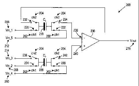
FIG. 2A illustrates a representative single-sampling
circuit 200 implementing the principles of an embodiment of
the present invention. The transfer function of circuit
200 is independent of capacitor mismatch, and can be
realized in a standard digital CMOS process requiring no
special options such as double poly or Metal-Insulator-
Metal (MiM) capacitors, expensive trimming or calibrations,
etc. It is based on delta-charge redistribution where the
only charge transfer (other than to an external load
capacitor) is to the parasitic capacitors at the amplifier
inputs. No charge transfer takes place via the virtual
CA 02494264 2005-O1-31
WO 2004/021251 PCT/US2003/026198
earth node of the amplifier, making the circuit inherently
accurate and second order independent of both the mismatch
and non-linearity of the signal capacitors. The circuit is
faster than prior art solutions due at least in part to the
buffer-type configuration used. Further, it has better
immunity to extraneous noise sources due to the fact that
there is primarily voltage processing with no
voltage-charge-voltage translations via the virtual earth
node which is a well-known pick-up point for unwanted
noise.
The representative single-sampling circuit 200 of FIG.
2A includes two opposite phased clock signals, namely clock
phases clkl 202 and clk2 204. The analog sampled data
input signals are shown as input signals Vin_1 206 and
Vin 2 208, and may be either direct current (DC) or time
varying signals. The signals Vin 4 210 and Vin_5 212 may
be either DC or time-varying signals. The signal Vin_3 214
may be used, for example, as a variable DC shift in order
to level shift the output signal Vout 216.
In operation, the input signal Vin_1 is sampled onto
capacitance C1 218 with respect to the reference voltage
Vin_5 212 on clock phase clkl 202 by closing switches 220
and 222. During clock phase clkl of the illustrated
embodiment, switches 224 and 226 are also closed to sample
the input signal Vin 2 208 onto capacitance CZ 228. In one
embodiment of the invention, bottom plate sampling is used,
where the input signals Vin_1 206 and Vin 2 208 are sampled
on to the bottom plate of capacitances C1 218 and CZ 228
respectively. The top plates of capacitances C1 218 and C~
228 are coupled to reference voltages Vin_5 212 and Vin_4
210 respectively during the clkl 202 phase.
On the next clock phase, clk2 204, C1 218 is coupled
across the amplifier 230 due to switches 232 and 234
closing, and switches 220 and 222 opening. Thus, the top
plate of capacitance C1 218 is coupled to the negative input
236 of the amplifier 230, and the bottom plate of
capacitance C1 218 is coupled to the output Vout 216 of the
amplifier 230. In one embodiment of the invention,
capacitance CZ 228 may be coupled at its bottom plate to
11
CA 02494264 2005-O1-31
WO 2004/021251 PCT/US2003/026198
Vin_3 214 by closing switch 238 on the clk2 204 clock
phase. Further, the top plate of capacitance CZ 228 may be
coupled to the positive input terminal 240 of the amplifier
230 on clk2 204 by closing switch 242. In this manner, the
voltage Vin_3 214 is coupled to the positive terminal 240
of the amplifier 230 through the capacitor CZ 228, in order
to provide voltage level shifting at the output Vout 216.
The transfer function for the single-sampling circuit
200 realization depicted in FIG. 2A can be determined using
voltage superposition, resulting in the transfer function
shown in Equation 4A:
:\
YoarLyaT~=Y" 3LyaTJ- v"_2 ~-~ -v't a ~-~ ~ + v" ~ ~-~ -~"_s ~ ~.
e~
EQUATION 4A
or alternatively written in Equation 4B:
~oar~~2'~=~" I~(h-~~~ v"-2~~~ 2 1 1+l"' 3~~Z'~+l;"_4~(~-~~~ Y" s~~~-2 J 1
EQUATION 4B
Typically, but not necessarily, the analog sampled
data input signals Vin_1 and Vin 2 are sampled with respect
to AC ground set at a reference voltage Vref. With this AC
ground 252 shown in FIG. 2B, and all signals referenced to
AC ground, the relationship between Vin_5 212 and Vin 4 210
of FIG. 2A becomes that shown in Equation 5 below:
1 1
~" a ~-2 ~=Y" s n-2 -0
EQUATION 5
which in turn provides the simplified transfer function
shown in Equation 6 below:
voar~~2''=Y" ~ j2-~ -l;"_2 ~-~ +I;'t_sLy~T~
EQUATION 6
12
CA 02494264 2005-O1-31
WO 2004/021251 PCT/US2003/026198
As can be seen, Equations 4A, 4B, and 6 are
independent of the capacitances C1 and Cz, illustrating that .
the circuits 200, 250 can provide a summing function
independent of capacitor mismatch that is inherently
exhibited in prior art solutions. No charge transfer takes
place via the virtual earth node of the amplifier, making
the design inherently accurate and second order independent
of both the mismatch and non-linearity of the signal
capacitors. Further, because the circuit configuration
primarily utilizes voltage processing with no voltage-to-
charge and charge-to-voltage translations via a virtual
earth node, the circuit configuration exhibits much better
noise immunity than prior art solutions. This makes the
circuit configuration suitable for use in standard digital
CMOS processes that are uncharacterized for analog
performance and have no special analog options.
Due to the accurate transfer function created by the
circuit configuration of an embodiment of the present
invention, it can be adapted to a double-sampling version
that is free of the typical, inherent problems of double-
sampling switched capacitor circuits that arise from
mismatch of capacitors. An example of such a double-
sampling circuit is shown in FIG. 3.
The representative double-sampling circuit 300 of FIG.
3 again includes two opposite phased clock signals, clkl
and clk2. The analog sampled_.data input signals are shown
as input signals Vin_1 302 and Vin 2 304, and the signal
Vin_3 306 may again be used as a variable DC shift in order
to level shift the output signal Vout 308. In this
example, the data input signals Vin_1 302 and Vin 2 304 are
sampled with respect to an AC ground.
In operation, the input signals Vin_1 302 and Vin 2
304 are sampled onto capacitances CZ 310 and C4 312
respectively on clock phase clkl by closing the appropriate
switches 314, 316, 318, and 320. The top plates of
capacitances Cz 310 and C4 312 are coupled to ground during
the clkl phase. On the next clock phase, clk2, Cz 310 is
coupled across the amplifier 322 due to switches 324, 326
closing, and switches 314, 316 opening. Thus, the top
13
CA 02494264 2005-O1-31
WO 2004/021251 PCT/US2003/026198
plate of capacitance C~ 310 is coupled to the negative input
328 of the amplifier 322, and the bottom plate of
capacitance CZ 310 is coupled to the output Vout 308 of the
amplifier 322. In one embodiment of the invention,
capacitance C4 312 may be coupled at its bottom plate to
Vin 3 306 by closing switch 330 on the clk2 clock phase.
Further, the top plate of capacitance C4 312 may be coupled
to the positive input terminal 332 of the amplifier 322 on
clk2 by closing switch 334. In this manner, the voltage
Vin 3 306 is coupled to the positive terminal 332 of the
amplifier 322 through the capacitor C4 312, in order to
provide voltage level shifting at the output Vout 308. As
can be seen, the operation is analogous to that described
in connection with FIGS. 2B.
The embodiment of FIG. 3 allows for the sampling of
the inputs Vin_1 302 and Vin 2 304 on a first clock phase
(e. g., clkl) and delivery of the output on a subsequent
clock phase (e.g., clk2) as described above. Further, in
accordance with the double-sampled embodiment shown in FIG.
3, inputs Vin_1 302 and Vin 2 304 can also be sampled and
delivered on alternate clock phases through the use of an
additional set of capacitors, whereby the input signals are
sampled on the second clock phase (e.g., clk2) and the
output delivered on the first clock phase (e.g., clkl). By
doubling the capacitors and making use of the alternate
clock phases in this way, it is possible to double the
processing rate of the circuit for the same analog power
dissipation.
More particularly, in the double-sampled embodiment of
FIG. 3, C1 336 and C3 338 perform similar functions to those
described in connection with CZ 310 and C4 312, but perform
these functions on opposite phased clock signals. Thus,
input signal Vin_1 302 is sampled onto capacitance C1 336
with respect to ground when switches 338 and 340 close,
which will occur on the opposite clock phase as when CZ 310
is sampled. On the same clock phase that Vin 2 302 is
sampled onto C1 336, Vin 2 302 is also sampled onto
capacitance C3 338 due to switches 342 and 344 being closed.
In this manner, Vin 2 302 is sampled onto capacitors Cl 336
14
CA 02494264 2005-O1-31
WO 2004/021251 PCT/US2003/026198
and C3 338 on the clock phase opposite to that in which
Vin 2 302 is sampled onto C2 310 and C4 312.
On the following clock phase, C1 336 is connected
across the amplifier 322 due to switches 346 and 348
closing. Thus, the top plate of capacitance C1 336 is
coupled to the negative input 328 of the amplifier 322, and
the bottom plate of capacitance C1 336 is coupled to the
output Vout 308 of the amplifier 322. On this same clock
phase, the bottom plate of capacitance C3 338 is coupled at
its bottom plate to Vin_3 306 by closing switch 350.
Further, the top plate of capacitance C3 338 may be coupled
to the positive input terminal 332 of the amplifier 322 on
this clock phase by closing switch 352. In this manner,
the voltage Vin_3 306 is coupled to the positive terminal
332 of the amplifier 322 through. the capacitor C3 338, in
order to provide voltage level shifting at the output Vout
308.
Using the additional circuitry in such a double
sampled embodiment, the inputs Vin_1 302 and Vin 2 304 can
be processed at double the rate of a single-sampling
implementation, thereby doubling the processing speed of
the circuit (assuming the same amplifier hardware is being
used) .
The example circuit 300 of FIG. 3 has a transfer
function shown by Equation 7 below:
~'o"tf~T~=~;"_~~(~-1)T~-~;"_Zf(~z-1)T~+r~" 3~~T~
EQUATION 7
The double-sampling circuit that can operate
independent of capacitor matching has a number of
advantages compared to the single-sampling version. For
example, the double-sampling circuit can operate at double
the speed of the single-sampling circuit for the same
frequency of non-overlapping clocks (e. g., clkl and clk2),
since the input can be processed on both clkl and clk2
phases. Even with this increased speed of operation, the
double-sampling circuit consumes the same analog power as
CA 02494264 2005-O1-31
WO 2004/021251 PCT/US2003/026198
the single-sampling circuit. Further, the double-sampling
circuit offers a full period delay, which is a requirement
for any sampled data system operating at a sampling rate of
1/T. Furthermore, a full period (T) hold signal is
possible when used as an interface from analog sampled data
to continuous time data. Since the single-sampling circuit
only has a delay of T/2, an extra delay of T/2 must be
found in order that all analog sampled data samples are
available at time intervals of T only.
The representative circuits described in connection
with FIGS. 2A, 2B, and 3 present balanced impedances from
.the capacitors and accompanying switches at the two
sensitive input terminals of the single-ended amplifier.
This ensures accurate settling between clock edges. As
previously noted, the transfer functions associated with
these circuits do not contain any capacitor ratios so that
the processing of the signals occurs independent of the
mismatch of the two signal capacitors with nominal value C.
Only errors of a second order nature occur due to the
presence of parasitic capacitances at the input nodes of
the amplifier. Any imbalances either between the
capacitors of nominal value C, or the input parasitic
capacitors, will give rise to an error that is second order
with respect to the absolute imbalance itself.
In accordance with one embodiment of the present
invention, various combinations of clock phase control may
be utilised. In the previously described examples, two
clock phases were described (e. g., clkl and clk2).
However, any number of desired clock phases may be used.
For example, using three clock phases clkl, clk2, and clk3,
a first of the voltage signals may be added at one clock
delay, where another voltage signal may be added at, for
example, two clock delays. This provides additional
variability and flexibility in the choice of delays. This
may be beneficial for circuit applications benefiting from
extended and/or variable clock delays. For example, delays
may be required in the case of filter design, such as with
Finite and Infinite Impulse Response (FIR/IIR) filters.
More particularly, such filters may be of an nth order
16
CA 02494264 2005-O1-31
WO 2004/021251 PCT/US2003/026198
where a plurality of previous inputs (in the case of non-
recursive filters) and/or a plurality of previous outputs
(in the case of recursive filters) are utilized to perform
the desired filtering function. Flexibility in delay lines
in the switched capacitor summer/level shifter in
accordance with an embodiment of the present invention is
highly advantageous. Therefore, where the transfer
function requires the addition of signals separated by one
or more delays, the addition of additional clock phases in
l0 accordance with an embodiment of the present invention
provides this ability.
FIG. 4 illustrates an example of an N-path sum-delay-
shift circuit '400 in accordance with one embodiment of the
present invention. Thus, where the additional clock phase
was used to facilitate double-sampling in the embodiment
illustrated in FIG. 3, additional clock phases may be used
for circuits requiring delays. The circuit of FIG. 4
operates similarly to the circuit described in connection
with FIG. 3, however additional switched capacitor circuits
are provided, as well as N clock phases. For example, N
switched capacitor circuits 402, 404, 406 are coupled to
the negative input 408 of the amplifier 410, and N switched
capacitor circuits 412, 414, 416 are coupled ~to the
positive input 418 of the amplifier 410.
The analog sampled data input signals are shown as
input signals Vin_1 420 and Vin 2 422, and the signal Vin 3
424 may again be used as a variable DC shift in order to
level shift the output signal Vout 426. In this example,
the data input signals Vin_1 420 and Vin_2 422 are sampled
with respect to an AC ground. In operation, the input
signals Vin_1 420 and Vin_2 422 are sampled onto
capacitances C within their respective N switched capacitor
circuits 402, 404, 406, 412, 414, 416. For example,
sampling for first switched capacitor circuits 402, 412
occurs on clkl, sampling for N-1 switched capacitor
circuits 404, 414 occurs on clkN-1, sampling for N switched
capacitor circuits 406, 416 occurs on clkN, and so forth.
On different clock phases, each of the switched capacitor
circuits can then be coupled across the amplifier 426 to
17
CA 02494264 2005-O1-31
WO 2004/021251 PCT/US2003/026198
perform the summing/level shifting function previously
described. In this manner, input signals may be added at
any desired delay, thereby facilitating realization of a
wide variety of different circuit implementations, such as,
for example, FIR and IIR filter circuits.
FIG. 5 is a flow diagram illustrating a method for
adding at least two input voltage signals in accordance
with the principles of an embodiment of the present
invention. A first input voltage signal is sampled 500
onto a first capacitor during a first clock phase.
Analogously, a second input voltage signal is sampled 502
onto a second capacitor during the first clock phase. On
the second clock phase, the first capacitor is switched 504
in order to connect to the negative input terminal of the
amplifier, and the second capacitor is switched 506 to
connect to the positive input terminal of the amplifier.
Also during the second clock phase, the output voltage is
fed back from the amplifier output to the negative input of
the amplifier by way of the first capacitor, as shown at
block 508. The sum of the first and second input voltage
signals is output 510 from the amplifier in response to the
feedback voltage, and in response to the first and second
sampled input voltages, during the second clock phase.
The signal processing capability of the method and
architecture in accordance with an embodiment of the
present invention enables its use in a wide variety of
applications where accurate addition and subtraction of
analog sampled data signals can be performed independent of .
capacitor mismatch. The transfer function is also
independent of non-linearity of the capacitors, since there
is only voltage sampling and no charge transfer takes place
from signal capacitor to signal capacitor. The only
significant charge transfer (other than that to the load
capacitance) is to the parasitic capacitors at the
amplifier inputs, which is only a small fraction of the
total charge held on the signal capacitors with nominal
values C. This, however, does not affect the accuracy of
.the transfer function. This is referred to herein as
18
CA 02494264 2005-O1-31
WO 2004/021251 PCT/US2003/026198
delta-charge redistribution, since the only main charge
transfer is that to charge parasitic capacitance.
The principles of an exemplary embodiment of the
present invention may be used in a wide variety of
applications, such as Finite and Infinite Impulse response
Filters (FIR and IIR filters), N-path filters, delay lines,
comb filters, integrators, differentiators, voltage
multipliers to any level, accurate inverters, level
shifters, voltage multipliers, single-to-differential and
differential-to-single ended converters, etc. These
functions can be realized with an order of magnitude
improved accuracy, and at least twice the speed than
previous circuits in standard CMOS processes (assuming the
use of similar hardware components).
It should be noted that any known circuit components
may be used to provide the operations in accordance with an
exemplary embodiment of the present invention. For
example, a capacitor may be used where capacitors are
indicated, however groups of series and/or parallel
capacitors may also be used. Further, other components
exhibiting capacitive properties and capable of storing a
charge thereon may be used. As another example, the
switches employed may be any component capable of
performing a switching function. For example, the
principles of an exemplary embodiment of the present
invention may be implemented using field-effect transistors
(FETs) and variations such as metal-oxide-semiconductor
field-effect transistor (MOSFETs), JFETs, VMOS, CMOS, etc.
Other transistor technologies may also be employed, such as
bipolar technologies. The switches may also be implemented
using electrically-controlled mechanical switches and/or
relays. Speed, efficiency, power consumption, and other
factors will determine the type of switches to be employed,
and in one particularly beneficial embodiment CMOS switches
are implemented to provide the desired speed and power
consumption characteristics. The amplifier components may
be any of a wide variety of operational amplifiers
facilitating single-ended operation.
19
CA 02494264 2005-O1-31
WO 2004/021251 PCT/US2003/026198
Use of Switched Ca~nacitor is ADC
Another exemplary embodiment of the present invention
is directed to an analog-to-digital converter (ADC) for use
in various ADC architectures, such as algorithmic and
pipelined ADC architectures. The ADC circuit in accordance
with the another exemplary embodiment of the present
invention provides a very accurate manner of
subtracting/level shifting, residue multiplication, and
sample-and-hold (S&H) functions, all within a single clock
cycle. In accordance with the invention, these functions
are performed using a switched capacitor technique that is
first order independent of capacitor matching. This
enables its use in new digital technology processes, such
as Complementary Metal-Oxide Semiconductor (CMOS)
processes, that are uncharacterized for capacitor matching
and analog performance.
In prior art ADC circuits such as 1.5-bit ADC stages,
charge transfer occurs from one input capacitor to a second
capacitor in the feedback look of an amplifier via the
virtual earth node of the amplifier. In this manner, the
input capacitor discharges to the feedback capacitor,
giving rise to an output voltage that is proportional to
the capacitor ratio (i.e., input capacitance/feedback
capacitance). For example, a gain of "2" may be created by
providing an input capacitor having a capacitance value
twice that of the feedback capacitor.
The another exemplary embodiment of the present
invention, on the other hand, adds capacitor voltages only,
with the amplifier serving as a buffer. For example, in
one particular embodiment of the invention utilizing 1.5-
bit ADC stages, a signal voltage may be sampled onto two
capacitors on one clock cycle. On a following clock cycle
one of the capacitors is placed in the feedback loop of the
amplifier, and the other capacitor is inverted and
connected between the amplifier's negative input terminal
and any one of a predetermined number of voltages used in
the 1.5-bit stage (e.g., +Vref, 0, -Vref), giving rise to
an effective doubling of the input sample voltage combined
with subtraction of one of the predetermined voltages. The
CA 02494264 2005-O1-31
WO 2004/021251 PCT/US2003/026198
resulting voltage is held at an output on a subsequent
clock cycle so that it can~be, for example, sampled by a
subsequent stage of a pipeline ADC, or sampled in once
again by a subsequent set of capacitors in an algorithmic
ADC. By summing only capacitor voltages and using the
amplifier as a buffer, multiplication by two, for example,
does not depend on the absolute values of the capacitors,
giving rise to a very robust solution suitable for
embedding in digital environments. Chip area and power
consumption are consequently reduced, thereby providing
enhanced power and area figures-of-merit (FOMs) compared to
current ADC designs.
A number of ADC architectures currently exist, and
design choices are often made based on parameters including
speed, power consumption, required real estate, complexity,
etc. For example, a straightforward and fast ADC
architecture is the flash architecture, where a number of
parallel comparator circuits compare sampled/held analog
signals with different reference levels. However, because
each reference level should be no further than one least
significant bit (LSB) apart, a large number of comparators
may be required for such an architecture. For example, an
N-bit ADC requires 2n comparators. Where the full scale
input is a relatively small voltage, the LSB size will be
relatively small, and the offset of the comparator needs to
be very small which may be difficult to achieve with
technologies such as CMOS, and special circuit techniques
may be required. Flash ADCs are therefore generally
limited to smaller resolution converters, such as 8-bit or
less resolution.
Two-step flash architectures arose to address some of
the problems of flash ADCs, where the two-step flash ADCs
first performs a course quantization, the held signal is
the subtracted from an analog version of the course
quantization, and the residue is then more finely
quantized. This significantly reduces the number of
comparators required in a standard flash ADC architecture,
but additional clock cycles are required to process the
signal due to the extra stage. Another enhancement arose,
21
CA 02494264 2005-O1-31
WO 2004/021251 PCT/US2003/026198
where interstage gain was used to tolerate larger
comparator offset for second stage comparators, which
ultimately led to the pipelined ADC architecture employing
multiple stages. The sampled input at each stage of a
pipelined ADC architecture is converted to a particular
resolution of the stage, such as n bits.
An ADC architecture resolving 1 bit per stage with
one-half bit overlap is referred to as a "1.5-bit" ADC
architecture. In order to facilitate an understanding of
the invention, various embodiments of the description
provided herein are described in terms of such a 1.5-bit
architecture. Examples of such architectures are set forth
below to provide an appropriate, representative context in
which the principles of the another exemplary embodiment of
the present invention may be described. However, it will
be apparent to those skilled in the art from the
description provided herein that the another exemplary
embodiment of the present invention is scalable and equally
applicable to other analogous ADC architectures.
FIG. 6 is a block diagram illustrating a typical 1.5-
bit ADC stage 1100. The circuit 1100 includes a sample-
and-hold (S&H) circuit 1102, a 1.5-bit sub-ADC 1104, a 1.5-
bit sub-DAC 1106, a subtractor 110, and a multiplier 1110.
Such an architecture is used in pipelined or algorithmic
ACS to provide maximum bandwidth and low sensitivity to
component mismatches. This is because each stage 1100
requires only two comparators (not shown) having an
accuracy of +/-(Vref/4) for the 1.5-bit sub-ADC 1104, and
one multiplier (e. g., amplifier) 1110. The associated
comparator and amplifier offset can easily be corrected
using standard digital error correction (DEC) techniques.
In the circuit of FIG. 6, the input voltage "In" is
sampled by the sample-and-hold 1102 and resolved into a
1.5-bit digital code in a course analog-to-digital sub
converter (sub-ADC) 1104. With a 1.5-bit sub-ADC, only
three codes are possible, such as 00, 01, 10. The
resulting 1.5-bit code 1112 is outputted to a digital error
correction circuit. The code is also converted, via a
digital-to-analog sub-converter (sub-DAC) 1106, back into a
22
CA 02494264 2005-O1-31
WO 2004/021251 PCT/US2003/026198
course analog signal with one of three predetermined analog
values, such as -Vref/2, 0, +Vref/2. The result is
subtracted from the sampled-and-held analog input signal
°In" via subtractor 1108. The resulting analog "residue"
is gained up by a factor of two using the multiplier 1110
to become the input voltage for the successive conversion.
As can be seen, the analog equivalent of the sub-ADC
1104 output plus the output residue (prior to
multiplication) is equal to the analog input voltage.
Thus, any perturbation in the residue due to non-idealities
can introduce differential nonlinearity (DNL) errors.
Effectively, all errors in the gained up analog residue
after the first conversion should be less than 1 LSB of the
remaining resolution of the ADC (or less than 2 LSBs of the
total resolution at N-bit level).
An N-bit algorithmic ADC 200 shown in FIG. 2 is formed
by sampling the input signal on the first clock cycle, and
sampling the output of the 1.5-bit stage 202 on the next N-
1 cycles. The 1.5-bit data 204 from each rotation are
added. up with 1-bit overlap in the DEC 1206 circuit such
that the least significant bit (LSB) from one rotation is
added to the most significant bit (MSB) from the next
rotation. Each rotation of the ADC resolves one effective
bit from the MSB level down to the LSB-1 level. The final
LSB bit is often resolved using a simple 1-bit flash 1208,
e.g., a comparator with its threshold set to OV. This bit
1210 is not added, but rather is concatenated to the
parallel data 1212 of the DEC 1206.
Alternatively, a series of such stages may be used to
create a pipelined ADC, such as the representative
pipelined ADC 300 shown in FIG. 8. The pipelined ADC 1300
includes a series of N-2 stages 1300, 1302,...1304, such as
those described in connection with FIG. 6, as well as an
Nth stage 1306. Stages 1300, 1302,...1304 may be used to
resolve N-2 bits, with the final stage 1308 being a 2-bit
flash to absolutely resolve the final two bits. The 1.5-
bit data 1310, 1312,...1314 and 2-bit data 1316 is provided
to the DEC 1318 to create the N-bit parallel output data
1320. The sample rate of the pipeline is approximately N
23
CA 02494264 2005-O1-31
WO 2004/021251 PCT/US2003/026198
times faster than that of the algorithmic architecture,
depending ultimately on what resolution flash converter is
used for the final stage 1308.
An example of a residue transfer characteristic of the
complete 1.5-bit ADC stage is shown in FIG. 9. In this
example, it is assumed that the full signal range is
between -Vref and +Vref. The transfer function is defined
by Equation 1 below:
Yout =2xV,.n +DxV,.ef
EQUATION 1
where D can take on any one of the values {-1, 0, +1}
depending on whether the analog input voltage falls within
corresponding ranges of
+ y.ef~ ~ + ref ' + ~rer ~ _ ref ' - ~rel~ ~ _~.e f
4 4 4 4
Vout of Equation 1 may either be resampled into the
algorithmic ADC on a subsequent rotation, or may become the
input voltage for a subsequent stage of a pipelined ADC.
In an actual implementation, the transfer
characteristic is affected by non-idealities in the analog
hardware. As previously indicated, offsets in the
amplifier and comparators can be corrected by the DEC. The
two remaining sources of error in an actual implementation
include inaccuracies in the creation of the multiply-by-two
(MX2) gain function (including subtraction of sub-DAC
levels), and variations in the reference levels.
Variations in reference levels are issues only in pipelined
ADCs, in which separate hardware in each 1.5-bit stage
samples +Vref and -Vref, where uncorrelated errors can
occur from stage to stage. Static errors in the reference
levels are not an issue for algorithmic ADCs, since each
rotation of the ADC samples the same references in the same
way with the same hardware. The absolute accuracy of the
reference levels is not important in a differential
implementation, as long as the reference levels are stable,
24
CA 02494264 2005-O1-31
WO 2004/021251 PCT/US2003/026198
within the usable dynamic range of the active circuitry,
and do not vary from conversion to conversion. At most,
the gain transfer is affected without affecting DNL/INL.
Thus, the only two remaining sources of error that limit
accuracy of the complete ADC are the accuracy of the
multiply (MX2) function and the DAC levels (sub-DAC). In
conventional implementations, this error is predominantly
caused by capacitor mismatch.
The combined accuracy of the MX2 and sub-DAC functions
must be better than one LSB of the remaining resolution of
the ADC in order to guarantee no missing codes. The first
stage of the pipeline has the most stringent requirement
here, as the MX2/sub-DAC functions for an N-bit ADC must be
accurate to at least N-1 bits, which is the number of bits
yet to be resolved after the first stage. The required
resolution of an N-bit algorithmic ADC is commensurate with
the required resolution of the first stage of a pipeline,
i.e., N-1 bits. For a robust design - and to account for
other sources of error, most notably noise - the accuracy
of the MX2 amplifier with sub-DAC, after including all
possible contributions of error, should be designed to be
at least 0.5 LSBs of the remaining resolution, i.e., N bits
accuracy.
The effect of a gain error in the first stage of a
pipeline, or the first rotation of an algorithmic, is
illustrated in FIG. 9. The comparator levels of the two
comparators of the 1.5-bit stage are set to -Vref/4 and
+Vref/4 respectively. It can be seen that when the gain of
the stage is too high, over-ranging can occur where the
slope 400 of the MX2 is greater than the ideal slope 402 of
the MX2. This causes the input signal to the next stage to
go beyond the maximum allowable range {+Vref and -Vref} for
conversion.
The effects on the complete transfer function of the
ADC are shown in FIGS. 10A, 10B, and 10C for gain errors
and sub-DAC errors in the first stage of a pipeline or in
the algorithmic ADC. FIG. 10A shows the effect of a gain
error greater than two in the MX2 which produces non-
monotonicity and the potential for missing codes. Where
CA 02494264 2005-O1-31
WO 2004/021251 PCT/US2003/026198
the ideal gain is equal to two as shown on dashed line
1500, non-ideal gain error greater than two as shown on
lines 1502A, 1502B, 1502C can result in missing digital .
output codes. Similarly, FIG. 10B shows the effect of a
gain error less than two in the MX2 which produces missing
codes. Where the ideal gain is again equal to two as shown
on dashed line 500 of FIG. 108, non-ideal gain error less
than two as shown on lines 1504A, 1504B, 1504C can result
in missing digital output codes. Further, FIG. 10C shows
the effect of sub-DAC errors in the first stage of the ADC
on the total transfer function. The ideal transfer
function is shown on dashed line 1506, and various
representative DAC level shift errors are shown on lines
1508A, 1508B, and 1508C, which will result in missing
codes. These errors are caused by capacitor mismatch and
non-linearity. In practice, all these errors will
propagate from the MSB to the LSB level, eventually (and
undesirably) producing a jagged transfer function for the
complete ADC.
Current 1.5-bit designs exhibit characteristics that
are responsible for much of this gain error. A switched
capacitor implementation of a 1.5-bit stage for a single-
ended application is shown in FIG. 11A, a portion of which
includes a prior art switched capacitor (SC) circuit 1600.
The switched capacitor circuit 1600 includes an amplifier
1602, two nominally equal capacitors Cf 1604 and CS 1606,
and several switches 1608, 1610, 1612, 1614, 1616, 1618,
1620. Two opposite phased clock signals, clkl and clk2,
are non-overlapping. The switched capacitor circuit 1600
performs the level shifting, residue multiplication by two
(MX2), and sample-and-hold buffering as is known in the
art. The input signal Vin is applied to the sub-ADC
including comparators 1622, 1624, with voltage thresholds
set at +Vref/4 and -Vref/4 respectively. Concurrently, the
input signal Vin is sampled onto CS 1606 and Cf 1604. At
the end of the first clock phase, clkl, Vin is completely
sampled onto CS 1606 and Cf 1604, while the output of the
sub-ADC 1622, 1624 is latched and held by latches
associated with the latches and clock generator 1626.
26
CA 02494264 2005-O1-31
WO 2004/021251 PCT/US2003/026198
During clk2, Cf 1604 is switched via switch 608 and placed
across the amplifier 1602, completing its negative feedback
loop 1628. At the same time, one of the input switches
1614, 1616, 1618 connected to CS 1606 is closed by the sub-
s DAC using only one of the clock signals top, mid, bot. In
this manner, the analog residue voltage is produced at the
output 1630, such that Vout is provided as shown in
Equation 2:
Cs
Your= 1+C XI;"+D>eTlrer
s
Equation 2
where:
Vin D BOt M1d TOp
vaa > I ;.ef ~ 4 - CS ~ C f 1 0 0
-1;.ef ~ 4 <_ Ya, 0 0 1 0
<_ +Vre f ~ 4
~a: ~ vref ~ 4 + CS ~ C~- 0 0 1
By choosing capacitors CS 1606 and Cf 1604 to have the same
value, Equation 2 is made to correspond to the ideal
transfer function of Equation 1 of a 1.5-bit stage. The
reference levels can be generated accurately and is
generally not a limitation on the realization of a high
resolution ADC (e. g., 12-bit level). The single factor
that ultimately determines the maximum resolution of the
ADC is the capacitor mismatch. This mismatch has two
effects on the performance of current state-of-the-art
designs, including 1) it affects the accuracy of the MX2
function, and 2) it affects the accuracy of the sub-DAC
through the accuracy with which the DAC levels {-Vref, 0,
+Vref} can be generated.
In order to achieve 10-bit performance, a matching of
the order of 0.1o is needed between CS 1606 and Cf 1604.
This is currently not possible to achieve in standard CMOS
processes without using special capacitor options, such as
the use of poly-poly capacitors. Even using such
specialized capacitors, very large values for the
27
CA 02494264 2005-O1-31
WO 2004/021251 PCT/US2003/026198
capacitors are needed (i.e., on the order of many
picofarads), to guarantee 0.1o matching across all process
corners. Such large value capacitors would be responsible
for creating an ADC that requires a great deal of real
estate and exhibits significant power consumption. For a
pipelined ADC with N-1 stages, such an approach is
unacceptable. Alternatively, calibration routines are
sometimes used to either trim the values of the capacitors
or to digitally calibrate out the gain error in a post-
processing routine. Such correction/calibration routines
are needed to achieve a resolution better than ten bits due
to the limitations of the processing technology on prior
art ADC circuit architectures. Complicated calibration
routines exist which add area, power consumption, and
latency to the conversion. Typically, many (e.g., up to
seven) clock cycles per bit are needed to calibrate away
capacitor mismatch errors. Still a further point of issue
can be capacitor linearity: any non-linearity in CS 1606 and
Cf 1604 of FIG. 11A will cause non-linearity in the MX2
amplifier 602 and cause differential nonlinearity (DNL) and
integral non-linearity (INL) errors.
For well known reasons of noise immunity and increased
dynamic range, conventional ADC solutions may be realized
using a fully differential amplifier. FIG. 11B illustrates
a differential switched capacitor implementation of a 1.5-
bit ADC stage. The conventional switched capacitor
implementation includes a differential amplifier 1650, as
well as a differential input signal Vin 1652 and a
differential output signal 1654. In such a conventional
differential amplifier implementation, the differential
amplifier 1650 is used, charge is transferred between
capacitors, and a capacitor ratio is still used to
establish the gain (multiplication by 2, for example). As
previously stated in the single-ended example, all of the
charge on one capacitor is transferred to the other
capacitor, and any error in the charge transfer results in
errors in the total transfer function. The capacitance
mismatch and non-linearity problems may be exacerbated
where double-sampling techniques are used. A double-
28
CA 02494264 2005-O1-31
WO 2004/021251 PCT/US2003/026198
sampling ADC stage may be realised that samples the inputs
on a first clock phase clkl and delivers its output on a
second clock phase clk2, and can also sample the inputs on
clk2 and deliver its output on clkl through the use of an
additional set of capacitors. By doubling the capacitors
in this way, it is possible to double the conversion rate
of the ADC for the same analog power dissipation. However,
in current state-of-the-art designs, double-sampling
introduces unwanted characteristics around half the
sampling frequency due to the extra mismatch that occurs
between both of the double-sampling channels from mutual
capacitor mismatch on clkl and clk2. To reduce such a
mismatch, the capacitors would need to be even larger than
in the single-sampling version, meaning more power and area
consumption which is undesirable. Mainly for these
reasons, double-sampling is often not used in current ADC
implementations.
The another exemplary embodiment of the present
invention addresses a number of shortcomings of prior art
ADC technologies, including the aforementioned error
situations exhibited by current ADC technologies. The
another exemplary embodiment of the present invention
significantly reduces errors in the MX2 (or other
multiplier) function, as well as errors in the generation
of DAC levels, that are present in conventional ADC
technologies. The another exemplary embodiment of the
present invention is first o--rder independent of capacitor
matching, enabling accurate, relatively high bit-width ADCs
in CMOS (and other technologies) that are otherwise
uncharacterised for matching of analog components.
Further, the apparatus and methodology in accordance with
the another exemplary embodiment of the present invention
allows for use of simple metal layer capacitors as the
signal capacitors, while still achieving accurate, high
bit-width performance. The another exemplary embodiment of
the present invention is also substantially faster than
prior art ADCs employing analogous hardware. Thus, with
use of similar amplifiers and capacitors in both prior art
systems and in the another exemplary embodiment of the
29
CA 02494264 2005-O1-31
WO 2004/021251 PCT/US2003/026198
present invention, the another exemplary embodiment is
substantially faster than the prior art systems by virtue
of the fact that the feedback factor (and, consequently the
gainbandwidth) for the amplifiers is substantially larger.
Referring to FIG. 12A, a block diagram of a
representative 1.5-bit ADC stage 1700 corresponding to a
first half of a differential implementation is illustrated.
FIG. 12B illustrates a second half of the representative
differential implementation. Two opposite phased clock
signals are used, namely clock phases clkl and clk2. First
considering the top half of the differential implementation
shown in FIG. 12A, Ink 1702 of the differential input
signal is sampled onto capacitance Cla 1704 with respect to
ground on clock phase clkl by closing switches 1706 and
1708. During clock phase clkl of the illustrated
embodiment, a number of other different switches are
closed, including switches 1714 and 1716. Thus, In n 1720
of the differential input signal is also sampled onto
capacitance C3a 1722 due to switches 1714 and 1716 being
closed during clock phase clkl. In one embodiment of the
invention, bottom plate sampling is used, where the input
signals Ink 1702 and In n 1720 are sampled on to the
bottom plate of the capacit'ances Cla 1704 and C3a 1722
respectively. The top plates of capacitances Cla 1704 and
C3a 1722 are coupled to ground during the clkl phase.
On the next clock phase, clk2, C1a 1704 is connected
across the amplifier 1724 due to switches 1726 and 1728
closing, and switches 1706 and 1708 opening. Thus, the top
plate of capacitance Cla 1704 is coupled to the negative
input 1730 of the amplifier 1724, and the bottom plate of
capacitance Cla 1704 is coupled to the output (Outs 1732)
of the amplifier 1724. Assertion of clock phase clk2 also
causes capacitance C3a 1722 to have its bottom plate
connected to any one of the voltages +Vref, 0, -Vref. Such
voltages are controllably selected by sub-DAC control
signals labeled as the top (top_a), middle (mid_a), or
bottom (bot a). The top plate of capacitance C3a 1722 is
then coupled to the positive input terminal 734 of the
amplifier 1724 on clk2. In this manner, one of the output
CA 02494264 2005-O1-31
WO 2004/021251 PCT/US2003/026198
control signals of the sub-DAC (i.e., bot a, mid a, top_a)
selects a corresponding +Vref, 0, or -Vref voltage, which
in turn serves as a reference voltage to the capacitance C~a
1722 during the second clock phase clk2. The net
consequence of these actions is that after one clock period
delay, Ink is added to an inverted version of In n, while
at the same time it is level shifted by either +Vref, 0,
-Vref. This is accomplished without ever creating a
transfer of charge between capacitors.
In a double-sampled embodiment, CZa 1736 and C4a 1738
perform similar functions to those described in connection
with C~a 1704 and C3a 1722, but with opposite phased clock
signals. More particularly, Ink 1702 of the differential
input signal is sampled onto capacitance CZa 1736 with
respect to ground on clock phase clk2 by closing switches
1740 and 1742. During clock phase clk2 of the illustrated
embodiment, In n 720 of the differential input signal is
also sampled onto capacitance C4a 1738 due to switches 1744
and 1746 being closed during clock phase clk2. In one
embodiment of the invention, bottom plate sampling is used,
where the input signals Ink 1702 and In n 1720 are sampled
on to the bottom plate of the capacitances CZa 1736 and C4a
1738 respectively. The top plates of capacitances CZa 1736
and C4a 1738 are coupled to ground during the clk2 phase.
On the next clock phase, clkl, Cza 1736 is connected
across the amplifier 1724 due to switches 1748 and 1750
closing, and switches 1740 and 1742 opening. Thus, the top
plate of capacitance C~a 1736 is coupled to the negative
input 1730 of the amplifier 1724, and the bottom plate of
capacitance Cza 1736 is coupled to the output (Outs 1732)
of the amplifier 1724. Assertion of clock phase clkl also
causes capacitance C4a 1738 to have its bottom plate
connected to any one of the voltages +Vref, 0, -Vref, in
response to the appropriate control output from the sub-
DAC. Such sub-DAC control signals are labeled as the top
(top_a), middle (mid_a), or bottom (bot a). The top plate
of capacitance C4a 1738 is then coupled to the positive
input terminal 1734 of the amplifier 1724. In this manner,
one of the output control signals of the sub-DAC (i.e.,
31
CA 02494264 2005-O1-31
WO 2004/021251 PCT/US2003/026198
bot a, mid_a, top a) selects the corresponding voltage
+Vref, 0, or -Vref, which in turn serves as a reference
voltage to the capacitance C4a 1738 during the first clock
phase clkl.
Using the additional circuitry in such a double-
sampled embodiment, the inputs Ink 1702 and In n 1720 can
be processed at double the rate of a single-sampling
implementation, thereby doubling the conversion speed of
the ADC using such circuit stages.
FIG. 12B illustrates a representative 1.5-bit ADC
stage 1760 corresponding to the second half of the
differential implementation described in connection with
FIG. 12A. The circuit stage 760 operates in an analogous
manner as that described in connection with FIG. 12A, using
another set of capacitances Clb 1762 and C3b 1764, as well as
capacitances CZb 1766 and C4b 1768 for the double-sampling
implementation. Further, because the circuit 1760 forms a
second half of a differential implementation, the input
signals Ink 1702 and In n 1720 are reversed such that the
input signal In n 1720 is ultimately coupled to the
negative input 1730 of the amplifier 1724, and the input
signal Ink 1702 is ultimately coupled to the positive
input 1734 of the amplifier 1724. The amplifier 1724
outputs the other differential signal, shown as output
signal Out n 1770 in FIG. 12B. Otherwise, the operation is
analogous to that described in connection with FIG. 12A,
ultimately producing differential output signals Outs 1732
and. Out n 17 7 0 .
FIG. 13 illustrates an implementation of the
differential ADC stage 1800 described in connection with
FIGS. 12A and 12B. The illustrated embodiment represents
an implementation of the differential ADC stage in the
context of an algorithmic ADC. In this embodiment, circuit
stages 1802 and 1804 correspond respectively to the
circuits 1700 and 1760 described in connection with FIGS.
12A and 12B. In this embodiment, all voltage levels are
shifted by a common mode voltage, refcm, such that the
signal range is between refn and refp. Therefore, a single
supply voltage may be used (i.e., 0 to Vdd). The
32
CA 02494264 2005-O1-31
WO 2004/021251 PCT/US2003/026198
illustrated ADC stage 1800 is applied in an algorithmic ADC
as previously described in connection with FIG. 7, with
non-overlapping clocks ADC_clk and ADC_clk n such that
ADC_c1k is high for one clock period and ADC_clk n is high
for the remaining N-2 clock periods as explained in
connection with FIG. 7. The differential analog input
signal (i.e., Ink 1806; In n 1808) is sampled at the start
of each conversion, using ADC_clk, while the gating with
ADC clk n ensures that the differential output signal
(i.e., Outs 1810; Out n 1812) is sampled for the remaining
N-2 clock periods. A final instantaneous decision can be
made with a 1-bit flash to determine the last bit, giving a
total of N-1 clock Cycles to resolve N bits.
Matching of the absolute values of reference voltages
-Vref/4 and +Vref/4, and consequently refp-refcm and refcm-
refn, is not needed in differential algorithmic/pipelined
ADCs. Furthermore, refcm may be nominally set halfway
between refp and refn, but its exact position is not
critical.
FIG. 14 illustrates a representative waveform diagram
corresponding to an algorithmic ADC such as described in
connection with FIG. 13. A master clock 1900 is provided,
where clkl and clk2 are non-overlapping phases of the
clock. For this algorithmic ADC, clocks ADC_clk 1906 and
ADC_clk n 1908 are non-overlapping, such that ADC_clk 1906
is high for one clock period and ADC_clk n 1908 is high for
the remaining N-2 clock periods. The data ready signal
(DRDY) 1914 is asserted when the ADC_clk 1906 is asserted,
thereby allowing the parallel data 1912 to begin
accumulating the associated digital data.
Non-overlapping clocks with early turn-off times,
i.e., _clkl a 1914 and clk2 a 1916, may be applied in the
implementation of the algorithmic ADC. When the capacitors
are sampling the input signals or references, the input
switches switching with respect to refcm switch off early
in one embodiment of the invention. On the other hand,
switches connecting the capacitors to the inputs of the
amplifiers should switch off late in accordance with this
embodiment of the invention. In this manner, when in
33
CA 02494264 2005-O1-31
WO 2004/021251 PCT/US2003/026198
cyclic mode, the outputs of the amplifiers can be sampled
~by the oppositely-phased capacitor networks before any
switching occurs around the amplifiers, ensuring clean
sampling.
An example of an ADC stage corresponding to a first
half of a differential, algorithmic ADC implementation,
such as that described in connection with FIG. 13, is
illustrated in FIGS. 15A and 15B. The example of FIGS. 15A
and 15B is provided as a representative implementation, and
those skilled in the art will appreciate that many
variations to such an implementation are possible.
FIG. 15A corresponds to the circuitry coupled to the
negative input of an amplifier, such as the switches and
capacitors coupled to the negative input of the amplifier
shown in block 1802 of FIG. 13. As was described in
connection with FIGS. 13 and 14, two opposite phased clock
signals are used, namely clock phases clkl and clk2. The
signal Ink 2000 of the differential input signal is
sampled onto capacitance Cla 2002 with respect to a
reference voltage such as refcm, on clock phase clkl 2004.
The signal 2000 is sampled onto C1a 2002 via switch circuit
2006. The ADC_clk 2008 enables the clkl 2004 to be passed
for one clock period,. via the NAND gate 2010 and associated
inverters 2012, 2014 to the CMOS switch 2016. Thus, when
the ADC_clk 2008 and clkl 2004 are asserted, the switch
2016 samples the Ink 2000 signal onto Cla 2002 with respect
to the reference voltage through CMOS switch 2018 when
switched by the early turn-off clock clkl a 2020.
On the next clock phase, clk2 2022, Cla 2002 is coupled
to the negative terminal 2024 of the amplifier via switch
circuit 2026. As previously indicated, the ADC_clk n 2028
is high for the remaining N-2 clock periods, thereby gating
the appropriate clock phase to the CMOS switch 2030 via the
logic components 2032, 2034, 2036, 2038. The output signal
Outs 2040, from the output of the amplifier (not shown),
is thus fed back to switch 2030 and coupled to the bottom
plate of the capacitor Cla on clk2 2022.
In a double-sampled embodiment, switch circuits 2042
and 2044 are also provided. These switch circuits 2042,
34
CA 02494264 2005-O1-31
WO 2004/021251 PCT/US2003/026198
2044 operate analogously to switch circuits 2006 and 2026
respectively, with the clkl 2004 and clk2 2022 signals
reversed with respect to switch circuits 2006 and 2026. In
the double-sampled embodiment, Ink 2000 is sampled onto
capacitance CZa 2046, and on the next clock phase Cza 2046 is
coupled to the negative terminal 2024 of the amplifier via
switch circuit 2048.
FIG. 15B corresponds to a portion of the circuitry
coupled to the positive input of an amplifier, such as the
switches and capacitors coupled to the positive input of
the amplifier shown in block 802 of FIG. 13. Because the
circuits associated with each of the capacitors Cja and C4a
in a double-sampling implementation of FIG. 13 are
analogous, only the circuitry of one such circuit is
described in FIG. 15B.
In n 2050 is sampled onto capacitance C4a 2052 via
switch circuit 2054. This occurs when clk2 2056 is high,
and ADC_clk 2008 is asserted on the first clock period of
the algorithmic implementation. NAND gate 2056 and
inverters 2058, 2060 enable passage of the In n 2050 signal
through the CMOS switch 2062 to be sampled on to C4a 2052.
On all remaining stages, ADC_clk n 2028 gates the clk2 2022
signal via switch circuit 2064, which includes NAND gate
2066 and inverters 2068, 2070, such that passage of the
Out n 2072 signal from the differential counterpart circuit
is enabled through switch 2074 to be sampled on to C4a 2052,
and ultimately switched via switch 2074 to the positive
terminal 2076 of the amplifier.
The sub-DAC provides control signals, such as bot b,
mid_b, and top b, which selectively provide a corresponding
voltage refp, refcm, or refn to the bottom plate of the
capacitor C4a via the level-shifting circuit 2078. In this
manner, one of the output control signals of the sub-DAC
.(i.e., bot la, mid_b, top b) allows a corresponding voltage
to level shift the voltage at the positive terminal 2076 of
the amplifier.
A counterpart circuit (not shown) corresponding to the
other half of the differential circuit shown in FIGS. 15A
and 15B operates analogously.
CA 02494264 2005-O1-31
WO 2004/021251 PCT/US2003/026198
Amplifiers that may be used in connection with the
another exemplary embodiment of the present invention, such
as amplifier 2724 described in connection with FIGS. 12A
and 7B, can retain a significant amount of residual charge
when switching from one N-bit conversion to the next. This
is due to the parasitic capacitance at the input to the
amplifiers, where this parasitic capacitance includes the
oxide input capacitance of the amplifier, wiring
capacitance, switch diffusion capacitance, etc. This
charge is transferred to the signal capacitors at the start
of the next new conversion, giving rise to a substantial
degradation in performance when any over-range occurs in
the ADC (i.e., an input signal which has an amplitude
larger than refp-refn).
In accordance with the another exemplary embodiment of
the present invention, a novel amplifier reset methodology
is implemented to address this residual charge problem
between conversions. In one embodiment, a number of reset
switches are timed to remove the residual charge on the
amplifier terminals, while performing the N-bit conversion
in N clock cycles of the master clock. As previously
indicated, by using a final flash stage it is possible to
convert an analog signal into a digital signal using N-1
clock periods of the master clock. The final decision is
instantaneous and becomes available with the final LSB+1
bit in the DEC. Thus,. during the sampling-in period with
ADC_clk (described in connection with FIGS. 13, 14, 15A,
15B), the amplifiers may be reset, since their output is no
longer necessary for the DEC. In this manner, the N-bit
conversion can be performed in only one additional clock
cycle, thereby resulting in an N-bit conversion in N clock
cycles of the master clock. If no such reset action were
performed, and the input were to fall below OV for example,
then the input signal must reach a minimum level of the
offset that has been transferred to the signal capacitors
before the ADC starts to convert properly again.
Therefore, the reset circuit used in connection with the
another exemplary embodiment of the present invention
36
CA 02494264 2005-O1-31
WO 2004/021251 PCT/US2003/026198
dramatically improves the performance of the algorithmic
ADC.
FIG. 16 illustrates a representative portion of an
algorithmic ADC stage 2100 which implements such a reset
circuit. The amplifier 2102, a single-ended amplifier in
the illustrated embodiment, includes a negative input 2104,
a positive input 2106, and an output 2108. As indicated in
connection with previously described embodiments, the
derived clock signal ADC_clk 2110 may be used to trigger
the initial sampling of the input signal in an algorithmic
ADC, and the derived clock signal ADC_clk n 2112 is used
for the remaining N-2 clock periods. During the time that
the new input signal is being sampled as enabled by ADC_clk
2110, the amplifier 2102 can be reset. It should be
recognized that the amplifier 2102 can be reset using an
additional clock cycle rather than during the sampling-in
period corresponding to the ADC_clk 2110, however resetting
the amplifier during this period allows the total
conversion to be minimized.
Thus, when the ADC_clk 2110 is asserted, each of the
switches 2114, 2116, 2118, and 2120 close, and discharge
any charge to a reference voltage 'which is refcm in the
illustrated embodiment. Reset switch 2114 is coupled
between the negative input 2104 of the amplifier 2102 and
refcm, and reset switch 2118 is coupled between the
positive input 2106 of the amplifier 2102 and refcm. A
reset switch 2116 is also coupled between the negative 2104
and positive 2106 inputs of the amplifier, which in turn
are coupled to refcm. Finally, reset switch 2120 is
coupled between the amplifier 2102 output 2108 and refcm.
When the ADC_clk 2110 is asserted (e. g., transitions high),
each of the switches 2114, 2116, 2118, 2120 are closed,
thereby discharging parasitic capacitances to refcm.
As indicated above, the ADC stage in accordance with
the another exemplary embodiment of the present invention
may be used in a differential implementation. However, the
principles of the another exemplary embodiment of the
present invention may also be implemented in a non-
differential mode. FIG. 17 is an example of how the
37
CA 02494264 2005-O1-31
WO 2004/021251 PCT/US2003/026198
' another exemplary embodiment of the present invention may
be implemented in a non-differential, single-sampling ADC
stage 2200. In this example, the input signal, Vin 2202 is
sampled onto a first capacitor C1 2204 when switches 2206,
2208 are closed during clkl. A complemented version of the
Vin 2202 signal is generated in any known manner,
represented by the inverter 2210. Thus, this inverted
signal, Vin' 2212 is sampled onto Cz 2214 during clkl when
switches 2216, 2218 are closed.
During the Clk1 phase, the Vin 2202 signal is also
received at the sub-ADC circuit 2220 of a level shifting
circuit 2230, where the sub-ACD Circuit 2220 provides the
1.5-bit (or other) data 2221, the value of which depends on
the Vin 2202 analog voltage level. This 1.5-bit digital
output is received by the decoder/Clock generator (Clkgen)
circuit 2222. On the next clock phase Clk2, the
deCOder/Clkgen 2222 asserts one of a plurality of control
signals based on the 1.5-bit data 2221, such as the
"bottom," "middle," or "top" signals. The asserted one of
the bottom, middle, or top signals closes a corresponding
one of the switches 2224, 2226, 2228 of the level shift
circuit 2230. Depending on which of the switches 2224,
2226, 2228 is closed, the corresponding reference voltage
-Vref, 0, +Vref is used to shift the output signal RESIDUE
2232 of the amplifier 2234, by providing the selected
reference voltage to the positive input 2235 of the
amplifier 2234.
The RESIDUE 2232 signal 2232 is generated during the
clk2 phase, where the sampled voltage on C1 2204 is coupled
between the output 2236 and the negative terminal 2238 of
the amplifier 2234, due to switches 2240 and 2242 closing
and switches 2206 and 2208 opening. Further, the sampled
voltage on CZ 2214 is coupled to the positive input 2235 of
the amplifier 2234 when switch 2244 closes in response to
clk2.
The Vin 2202 signal is therefore inverted, and the
complementary signals Vin 2202 and Vin' 2212 are sampled,
and provided to the amplifier 2234 as the Vin 2202 signal
and an inverted version of the complemented Vin signal, to
38
CA 02494264 2005-O1-31
WO 2004/021251 PCT/US2003/026198
provide the MX2 function by adding these signals. The
RESIDUE 2232 is provided as a result of the subtraction of
the voltage provided by the level shift circuit 2230 and
the MX2 function performed at the amplifier 2234. As can
be seen, the subtraction/level shifting, residue
multiplication by two, and sample/hold functions are all
performed in one clock cycle, independent of any capacitor
mismatch that may occur between the signal capacitors C1
2204 and CZ 2214.
It is noted that the sub-ADC 2220, decoder/clkgen
2222, and level shift circuit 2230 are representative of
the circuit (or equivalent thereof) that may be used to
provide the coarse analog-to-digital conversion, decoding,
and level shift functions for any of the embodiments of the
present invention described herein.
FIG. 18 is a flow diagram of a method for converting
an analog input signal to a digital input signal in
accordance with one embodiment of the present invention.
The analog input signal is sampled 2300 onto a first
capacitor, or group of capacitors or capacitive elements
collectively providing a capacitance in which the input
signal may be stored. A complemented analog input signal,
i.e., an inversion of the analog input signal, is similarly
sampled 2302 onto a second capacitor(s). One or more
switches are actuated 2304 in order to couple the first
capacitor between the amplifier output and a first
amplifier input, in a unity gain feedback arrangement. The
sampled input signal is thus provided to the first
amplifier input, such as the inverting/negative amplifier
input. One or more switches are also actuated 2306 in
order to couple the second capacitor between a selected
reference voltage and a second amplifier input, in order to
provide an inverted version of the sampled complemented
input signal to the first amplifier input as level-shifted
by the selected reference voltage. The sampled input
signal is added 2308 to the inverted version of the
complemented input signal using the amplifier, and the
selected reference voltage is effectively subtracted from
39
CA 02494264 2005-O1-31
WO 2004/021251 PCT/US2003/026198
the output in order to provide a residue signal available
for use in subsequent conversion stages.
If there are more ADC residue stages in the ADC as
determined at decision block 2310, then the next stage 2312
is considered, and the process is repeated for that stage.
When there are no further stages, such as when N-1 stages
have been processed in an algorithmic or pipelined ADC
configuration, then the final flash stage can be processed
2314 as previously described.
Each of the illustrated embodiments (as well as other
embodiments of the present invention not illustrated
herein) not only provide a significantly more accurate
conversion, the resulting ADC is substantially faster than
prior art ADCs employing analogous hardware. In other
words, the use of amplifiers and capacitors in both prior
art systems and in the another exemplary embodiment of the
present invention, the another exemplary is substantially
faster than the prior art systems by virtue of the fact
that the feedback factor (and, consequently the
gainbandwidth) for the amplifiers is substantially larger.
The foregoing description of various exemplary
embodiments of the invention has been presented for the
purposes of illustration and description. It is not
intended to be exhaustive or to limit the invention to the
precise form disclosed. Many modifications and variations
are possible in light of the above teaching. It is
intended that the scope of the invention be limited not
with this detailed description, but rather by the claims
appended hereto.