Note : Les descriptions sont présentées dans la langue officielle dans laquelle elles ont été soumises.
CA 02494336 1994-07-21
RADIOTELEPHONE SVSTEM FOR GROUPS OF REMOTE SUBSCRIBERS
Field of the Invention
This invention relates to radiotelephone systems for
serving a plurality of remote subscriber stations and, more
particularly, to a radiotelephone system in which certain
of said subscriber stations are located in a physically
adjacent group.
Background of the Prior Art
A radiotelephone system including a base station for
serving remote subscriber stations is described in U.S.
patent 5,119,375. In that system each subscriber station
was equipped with a radio that could be instructed by the
base station to tune to a particular channel and to employ
a particular time slot for the duration of a given
conversation. Time division multiplex (TDM) radio channel
transmission was employed from the base station to the
subscriber stations and time division multiple access
(TDMA) transmission from the individual subscriber stations
to the base station. The time division of each radio
channel into time slots and the compression of speech
signals permitted each radio frequency channel to support
a number of voice paths equal to the number of time slots.
Analog voice signals to and from the public switched
telephone network were first converted to 64 kbps ~.c-law
companded pulse coded modulation (PCM) digital samples.
Before transmission over the radio channel the digital
samples were subjected to voice-compression to reduce the
voice information rate from 64 kbps to 14.6 kbps using
residual excited linear predictive (RELP) coding. A voice
codec and modem were required to be dedicated to a specif is
frequency and time slot for the duration of a call.
While the foregoing system operated in a highly
satisfactory manner in allowing telephone service to be
provided especially to areas where wire lines are
CA 02494336 1994-07-21
=2-
impractical, the unforeseen growth of such telephone
service has given rise to sitii~tions iii which Several
subscriber stations are found to lie in close proximity
with one another. Initial efforts to lower) the per-line
, cost of serving a group of~such closely situated subscriber
stations were focused on consolidating the installation and
maintenance costs of individual, subscriber stations through
the sharing of common equipment such as~the enclosure,
power supply, RF power amplifier and antenna. Thus, in a
to closely situated group of subscriber stations, each of
which could access an RF channel,, a single broadband RF
power amplifier could, be employed to serve the group.
However such efforts still required each subscriber line to
have its own modem anc~ radio transceiver.. . 'fhe individual
transceiver outputs were fed to the common RF~ power
amplifier, which had to be designed to handle's peak power
equal to the sum of the power of all,of the~transceivers in
.;.
the group of adjacent subscriber stations~~that could
simultaneously be active on the~~same time slot. It is
apparent that further consolidation over that possible in
the '375 patent system and a reduction.in the~peak and
average power required would be~desirable, especially in
remote areas required to be served by,solar cell power.
Summary of the Invention
25' ' In accordance with the principles of our invention,
per-line costs are reduced for a physically adjacent group
of subscriber lines by perTnitting. the lines within such a
group to snare not only a common.poWer~supply and RF power
amplifier, but modem, synchronization,, IF, izp-.and down-
conversion and controller functions ,'as ~well~, so that
significant concentration is achieved. . In our, system, a
small number of modems is provided .to se.i-ve the multiple
subscribers in a physically adjacent, group, hereinafter
referred to as cluster or, more particularly, as~a modular
cluster. In an illustrative embodirrient, subscriber line
CA 02494336 1994-07-21
circuits and modems are modularized printed circuit cards
which plug into a frame employing backplane wiring to
distribute timing information and data among the units.
Any of the modems may be seized to handle a call for any of
the subscribers and each modem may handle calls for several
subscribers on succ6ssive time slots. The same or a
different freauency may be used to support communications
for each subscriber on successive time slots.
It is a feature of our invention that the selection
to from the common pool of frequency-agile modems of the modem
to be used to handle a call is controlled to conserve power
consumption in two ways. First, a new modem is preferably
not seized far use to handle a call until all of tha time
slots on active modems have been assigned to calls, thereby
allowing all not-yet-selected modems to remain in a power-
conserving, "powered-down" state.
Second, the number of calls using the same time slot (on
different frequencies) is controlled to reduce the peak
power demand on the RF power amplifier.
It is a further feature of our invention to avoid
synchronization delay when it is necessary tv seize a
powered-down modem for use on a call. Once time slot
synchronization with the base station has been established
for the first modem of the pool at the cluster,
synchronization information is made available to the
remaining modems, advantageously over backplane wiring,
under control of a microprocessor-based cluster controller.
Accordingly, all powered-down modems remain instantly
assignable to handle calls without undergoing any delay to
become synchronized with the base station's time division
frame.
It is a further feature of our invention to classify
modem synchronization states according to several
synchronization parameters and to derive a confidence
factor =or each active modem that reflects the reliability
of the synchronization parameters and to distribute
CA 02494336 1994-07-21
-4-
s~rizch~onizatiorl information from the mddeiti ha~iihg the best
cdr~f ideace factor .
Brier Description of the Drawiricts
The foregoing and other ob~eCta and features of our
invention may become more appdtent by referring now to the
drawing iri ia3lich : '
Fig. 1 is a block diagraM of a hlodttlar cluster having
a common pool of frequency agile modems for handling a
group of subscriber stations;
1o Fig. 2A shows the aseoCi2.tion' of stLbsdriber line
circuits and modems at the time slot interchahger;
Fig, 2H shows the TDMA RF frame allocated for I~PSK
time slots; ' ' '
Fig . 2 C shows the TDMA RF frame allocated for QPSK
time slots;
Fig, 2D shows the task scheduling between the TDMA
time slots and the PCM buffers;
Fig. 3 shows the principle circuit elements of a
frequency agile modem module;
Fig. 4 shows the IF portion af"the frequency agile
modem;
Fig. 5 is a block diagram of the block synthesizer,
up/down converter;
Fig.'& shows the frequency synthesis and noise shaper
2S for the receiver portion of the modem;
Fig. 7 shows the frequency synthesis, modulation and
noise shaper circuitry for the IF'transmitter portion of
the modem; and
Fig. 8 shows the system clock generation circuitry for
3o the modular cluster.
General Description
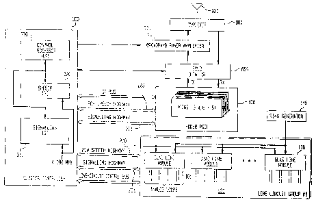
Fig. 1 is a block diagram of a modular subscriber
cluster that is located remotely from a base station (not
CA 02494336 1994-07-21
_$_
shown). The subscriber cluster is termed "modular" because
the line circuits 100 and the modems 400 are comprised of
plug-in units. Accordingly, the number of plugged-in
subscriber line circuits 100 will depend on the number o~
subscribers in the locality and the number of plugged-in
modems 400 may be traffic-engineered to handle the amount
of traffic expected to be generated by the number of line
circuits 100. Line circuits 100 are contained on quad line
module cards 101-108, each of which serves four subscriber
lines. Eight such quad line modules provide loop control
functions to a line group of 32 subscriber lines and
circuits 100 may contain multiple line groups.
Each line circuit on each quad line module 101-108 is
given a dedicated PCM time slot appearance in PCM speech
highway 200 and in signaling highway 201. The quad line
modules 101-108 include voice codecs (not shown? to encode
subscriber loop analog voice onto PCM data highway 200.
Subscriber loop signaling information is applied to
signaling highway 201 by a subscriber line interface
circuit SLIC (not shown). Either ~C-law or A-law PCM coding
may be used.
The connection of a particular one of modems 400 to
handle a call from ox- to a particular one of the line
circuits on one oz quad _ine modules ? O1-108 is made via
time slot interchangers 310 and 320, as instructed by
cluster controller 300. PCM data time slot interchanges
320 conveys speech samples between the PCM speech highway
200 serving line modules 101-lOB and the Pr'M speech highway
220 se raring modem pool 400. signaling time slot
interchanges 310 conveys signalling information between
signalling highway 201 serving the modules 100 and
signalling highway 221 serJing modem pool 400.
Two RF channels are required for a telephone
conversation, one for transmissions from the base stat~.on
to the subscriber (the 'forward' channel) and one from the
subscriber to the base station (the 'reverse' channel).
The forward and reverse channel frequencies arm assigned by
CA 02494336 1994-07-21
-6-
the telecoinmunicatione authority and in a typical example
may be separated from each other by 5 MHz. The path of the
forward. chanziel radio signal received at the cluster from
the ba.ee station may be traced frorri cl~ieter antenna 900 and
~5 dunlexer B00 to block synthesizer up/down converter (BSLFD)
600; In block converter 600 the RF signal is limited,
band-pass filtered and down-converted from the 450 MHz, 90D
I~z or other high, or ultra-high frequency RF band to an IF
signal in the 25 - 28 M~z range. ~ The IF signal is
l0 delivered to modems 400 whieh process the signal for
delivery to the subscriber liz~e circuits via the time slot
interchangers in the cluster controller 3oD:
The modems each.inc~i~de a baeebahd~digital signal
processor (gee Fig. 3, DSP/HH) and a mbderd' ~roceseor (see
15 Fig : 3 , DSp/MDi~I) : In the forsriard channel direction; modem
proCessoz- DSP/MDM demodulates the IF signal received from
block Converter 600 and transfers the data to 'baseband
processor DSPJEB which expands the demodulated data into ~.-
lAw or A=law encoded signals for transmisaiori through time
20 slot interchanges 320 to the line modules: The modem's
baseband processor DSP/HB interfaces to modem prbcessor
DSP/MDM via a direct memory access DMA) interface (see
Fig. 3) and to the PCM highways through the processor's
serial port. In the reverse channel~direction, baseband
25 processor DSP/HB conlrerts the u-lac~i or A-law coded PCM
infoririation received from PCM highway 500 into linear form,
ccsmaresses the linear data usirig'~RELP coding and DMA
transfers the compte9sed data to digital signal processor
DSP/NIDM which modulates the signal for transmission on the
30 radio channel time slot.
As shown in Fig. 2A, each of modems 400 and each of
line modules 100 has four dedicated time slot appearances
in PCM data time slot interchariger~320 for non-blocking
access. Each modem is assigned two adjacent PCM slots in
3 S PCM time slots 0-15 and two s.djacent PCM time slots in PCM
time slots 16-31. As an example, for a particular call,
TSI 320 connects ,line circuit 0 of line ' module '-101 to
CA 02494336 1994-07-21
channel 1 of modem 1, and line circuit 1 of line module 101
is connected to channel 0 of modem 1, and so on. Time slot
ir_tercharigers 310 and 32b provide a repetitive 125 ~.S
sampling period containing 32 time slots operating at a
rate of 2.048 Mbits/sec. During each I25 ACS PCM interval,
the line modules may send thirty-two, 8-bit bytes of data
to time slot interchanger 320 and each modem may receive
four of the 8-bit bytes at its baseband processor serial
port, packed together as two 16-bit words. Each ls-bit
lb word causes. a aerial port interrupt on the baseband
processor. When the interrupt is received, the baseband
processor determines whether the pair of PCM samples
contained in the 16-bit word correspond to slots 0 and 1 or
to slots 2 and 3. Similarly, during each 125 ~.S PCM
interval, four voice channels of PCM data, packed together
as two 16-bit words, may be sent from each baseband
processor's serial port to time slot interchanger 320 for
delivery to the line modules.
The TDM (RF) frame at the base station is shown in
Figs. 2H and 2C, each having a duration, illustratively, of
45 ms. The 16PSK frame of Fig. 2B has four time slots,
each of duration z, each time slot capable of carrying the
diif erent frequencies assigned to the forward and reverse
channels of the call. In Fig. 2C the RF frame of the same
duration is capable of accommodating the forward and
reverse channels of two QPSK modulated calls. It can be
appreciated that, alternatively, the TDM frame can carry
four 16PSK calls or two QPSK modulated calls.
Fig. 2D illustrates the timing of the tasks performed
3o at the cluster in conveying information between an
illustrative TDM.A frame carrying QPSK modulated calls and
the DCM highway frames . Line (1) represents the buffers for
receiving the two QPSK modulated forward channel time
slots, Rxl and Rx2, of th= TDM-~. frame. Demodulation is
begun as soon as the receive buffer has received the first
half, Rxla, of the time slot. Line (2) represents the
buffers preparing. to transmit in the two reverse charnel
CA 02494336 1994-07-21
_g_
QPSK tirtie 9lota, Txl and Tx2, of a TDMA frame: Note that,
at the Cluster, the reverse channel time slots are offset
from the forward channel time slots so that the subscriber
station may avoid the expense 2.nd bulk of a duplexer, In
addition, the subscriber unit's the reverse channel will be
offset so that it tvill be received at the bade station at
the pxoper time taking into accotlrit 'the' digts.rice between
the etibscriber station and the base station , Lines (3 ) and
(4) of Fig, 2D represent the buffers in the,SRAM (Fig. 3)
IO of the modern whieh store the PCM taords to and from speech
time slot interchanger TSI 320 (Fig. 1).
In normal voice operation, the modem processor DSP/MDM
demodulates received forward channel symbols, packs them
into a buffer ~n SRAM/Nmrt and sends the contents of the
I5 buffer to the baseband proceseot DSP/HB for KELP synthesis
(expan.sion): The baseband processor encodes the expanded
data to (l-last or A-lair and ptit~ it an the PCM bus for
delivery to the line mot3ules. 'Voice code Words are
transtrlitted iii every frame during active vbice operation.
20 The code trord resides at the beginning of the burst between
the r~reamble and voice data on both the forward and reverse
channels. The forward channel voice code words contain
information that may be used to adjust transmit power and
timing. Local loop control information (i.e.,- unhook,
25 offhook, ring, forward disconnect) .'is also embedded in
these code ~tords. The reverse charnel code words contain
subscriber station local loop control and forward channel
link quality information.
The fortaarci voice codewotd i5 decoded by the modem
30 prdcegsor DSP/t'~M. The forward voice codeword contains
transmit fractional timing control,"transmit power~level
control and local lbop .control information: The fractional
timing and power level control information is averaged out
over a frame and the average adjustment made at the end of
35 the frame. The local loop control information is stored
locally and changes in loop state are detected and reported
to the cluster controller. The local loop control also
CA 02494336 1994-07-21
_g_
causes the modem to send out line circuit control over the
signalling bus. The reverse voice codeword contains local
loop status that is used by the cluster controller and base
station to monitor call progress.
S The modem processor DSPjMDM performs receive FIR
filtering and automatic gain control of the received
samples during a receive symbol interrupt service routine.
The demodulator routine in the modem processor is called
when half a slot of baseband information has been received
to in the receive buffer. The demodulator operates on the
half slot of data and passes the packed output data to the
baseband processor DSP/BB for KELP synthesis. Data
transfer to and from the baseband processor is controlled
so that the KELP input queues are filled before the
15 corresponding synthesis data is required, and RELP output
aueues are emptied beTore new analysis (compression) output
data arrives. During demodulation, automatic frequency
control (AFC), automatic gain control (AGC?- and bit
tracking processes are performed to maintain close
20 synchronization with the base station.
It should be appreciated that mixed mode operation is
aossible whereby some time slots in the RF may employ loPS~C
modulation while the remaining slots employ QPSK
modulation.
25 S~mchronization to the Base Station
Before an RF channel can be used for communication
between the base station and the cluster, the cluster must
be synchronized to the RF time slot scheme used by the base
station (not shown). In accordance with our invention, one
30 or more of modems 4oo will be ordered by cluster controller
300 to acquire synchronization with the base station RF
frame timing by searching for the channel frequency
carrying the radio control. channel (RCC? being used by the
base station. Cluster controller 300 includes a master
35 control microprocessor 33Q, illustratively, one employing
CA 02494336 1994-07-21
-10-
a Motorola 68000 series processor, which ~eendg~ control
information over the CP bus to the microprocessors in
modems 400. On power tip, cluster controller 300 down-loads
appropriate software and initialization data to modems 400.
After the channel frequency is found; the modem must
synchronize with the base station time slot by decoding the
RCC unique word: As described in the aforementioned '375
patent, the RCC channel is distinguished from other
channels in that it hoe an extended guard interval: during
its time slot.and includes a DBPSK modulated'unique word of
8 bits. In order to minimize the possibility of aborting
a call if the modem with the active RCC time slot fails and
it becomes necessary to assign the RCC time Blot to a
different modem, time slots are assigned laithiil~an active
modem eo that the synchronization (RCC? time slot ~ (referxed
to as Rx0 Where the four time slots - ~ acre ~ nuiiibered . Rx0
~throughw Rx3, or Rxz.. where. the ' time slots are number Rx1
through Rx4); is the last to be~~illed:
At start-up, all of htoderrts 400 are- assumed to be out
of synchronization with the base stat~.on' a RF 45 c~is frame .
During tune slot zero of the RF frame,~the base station
transmits an RCC message on some Rf channel which;'when
received at the modular cluster, ~ will be decoded to put the
cluster into synchronization with the base station's RF
time slot frame for all RF channels. Until synchronization
with the base station is achieved, each modern generates its
own local RF frame sync. Cluster controller 300 next
commands one or more moderns to hunt for the RGC transmitted
by the base station on different RF tharmelW until the RCC
is found or all channels have been ~seatched. If all
channels have been searched and the RCC has not been found,
the controller orders the search to begin again.' When a
ti~odem finds the RCC, the controller designates it ~as the
RCC modem and distributes its sync inforrria.tion to the
rernairiirig modems via the frame sync signal over the
backplane_
CA 02494336 1994-07-21
-11-
When the RCC slot search is undertaken, the channel
number is used by the modem to digitally sweep a direct
digital frequency synthesis (DDFS? local oscillator,
illustratively over a 2 I~C-~z range. There are two stages to
a modem's acquisition cf the RCC channel, coarsely
identifying the center frequency and finding the "AM hole",
a portion of the RCC time slot where the number of symbols
transmitted by the base station does not fill up the entire
slot time. Coarse frequency acquisition is based on
l0 performing a Hilbert transform of the spectrum of the RCC
channel which yields a frequency correction for the local
oscillator. This continues until the energy in the upper
half of the spectrum approximates that in the lower half.
After coarse frequency acquisition is obtained,
25 illustratively to within an accuracy of 300 Hz o~ the
channel center freauency, a search is made for the ~1M hole .
A number of null signals are transmitted prior to the RCC
data., The AM hole is identified by monitoring the
amplitude of consecutive received symbols. When twelve
20 consecutive null symbols are detected, an AM strobe signal
is output by the modem to indicate the start of an RCC slot
and the start of a TDMA frame. This coarsely synchronizes
the baseband modem timing to the base station timing.
Synchronization need only be performed once since the radio
25 link is shared by all baseband modems in the modular
cluster. The frame sync signal is sourced by one modem to
all other modems in the cluster via a signal on the
backplane wiring. During the search for the RCC if the AM
hole is found to within 3 symbol periods of the start of
30 frame marker, coarse acquisition is complete. The location
of the unique word within the frame provides the modem with
timing information that is used to bring the modem's local
frame timing to within one symbol timing of the base
station. The modem is said to be in receive sync, Rx RCC,
3S as long as it continues to receive and decode the u_niaue
word correctly. Once synchronization is achieved, 16PSK
modulation corresponding to 4 bits per symbol, QPSK
CA 02494336 1994-07-21
-12-
modulation cotresponding to 2 bits per symbol, or
combinations of both may be employed.
While all modems are capable of receiving and
synchronizing to the base station's radio control channel
RCC, only one modem need do this since the modem which is
selected by the cluster Controller can share its timing
with the other modems vii. the Frame Sync signal over the
backplane fairing. The selected modem will source the Frame
Sync Dut signal and all other modems will. accept this
signal as the Frame Sync In signal.
When a modem goes on line, its modem processor DSPJMD~!
instructs its DDF .450 (Fig. 3? to try to synchronize its
local frame timing to the backplane signal. Each modem's
DDF 450 timing is at this moment independent of every other
modem's timing. DDF 95o will initially be ingtructed~by
its DSP/c~M to look at the backplane signal for its
synchronization.. If a backplanc synchronization signal is
present, the DDF will synchronize its~frame sync signal to
the backplane signal and then disconnect from the backplane
eignal_ The bacicplane signal thus does not feed directly
into the modem's timing circuitry but merely aligns the
modem's internal start of receiire frame Hignal. If a
backplane synchxonization signal tras not present, it is
assumed that~the modem is the first one that has been
activated by the cluster controller, in Which case the
cluster controller 30o will inetrttct the modem processor
DSP~MDM to look for the RCC and ~enc~ the modem's timing to
the cluster controller.
Cluster controller 300 next instructs the modem
3 p processor DSP~t~'mM to demodulate the DBPSK signal on the RCC
Cliahiie7.. The path for demodulation o~ the ~IF signal
received~from block converter s00 may be traced to the
modem IF modi~? a Where it is again band-pass filtered and
down-converted to a 16 kilosymbol peg second in~ortnation
stream. The DHPSK modulation that is employed on the RCC
channel z9 a one bit per symbol modulation_ The RCC
messages that a.re . received from the base station must be
CA 02494336 1994-07-21
-13-
demodulated and decoded before being sent to the cluster
controller. Only messages that arm addressed to the
cluster controller, have a valid CRC. and ars a burst type
message or an acknowledgment message are zorwarded to the
S controller. All other messages are discarded. An
acknowledgment message signifies the correct reception of
the previous RCC message. A message is addressed to the
cluster controller if the Subscriber Identification number
(SID) contained in the message matches the SID of the
l0 cluster.
Referring to Fig. 3, the 16 kilosymbol per second IF
signal from the IF circuitry of Fig. 4 is entered into A/D
converter 804, which is sampled at a 64 KHz rate by a clock
signal received from DDF chip 450. A/D converter 804
15 performs quadrature band-pass sampling at a 64 kHz sampling
rate. Quadrature band-pass sampling is described, inter
alia, in US patent 4,764,940. At its output, converter 804
provides a sequence of complex signals which contains a
certain amour_t of temporal distortion. The output of
20 converter 804 (Fig_ g) is entered into RxFIFO in DDF chip
450. Modem processor DSP/MDM reads the contents of RxFIFO
and performs a complex FIR filtering operation, which
removes the temporal distortion introduced by the
quadrature band--pass sampling. After the removal or
25 temporal distortion, the signals are demodulated by
procssor DSP/MDM.
During the demodulation of RCC messages, AFC, AGC and
bit tracking processes are perfomed by modem processor
DSP/MDM to maintain the cluster in close synchronization
30 with the base station. Transmit timing and power level
adjustments are made according to infoz;nation received in
the RCC message. Processor DSP/MDrI examines the
demodulated data and detects the RCC message, a message
~~rhich includes link status bits, and 96 bits of data that
35 includes the subscriber ID. Modem processor DSPJMDM also
recognizes whether the subscriber ID belongs to one of the
subscriber line circuits in the cluster.
CA 02494336 1994-07-21
_ltj._
tf, .the message is fot~ this cluster ,"'the ~ me~shge is
passed to clusteb controller 300, which interprets the RCC
comriiand. Forward RCS mesgageS iaclilde page message, a call
connect, clear indication and'self=test. ~ ftevexse RCC
S messages include call accept, clean requestj'test results
and fall req-iieet: If the RCC Message is 'a page message;
the cluster controller for tvhich it'is designated will
formulate a call dccepted message to be~transmitted back to
the base station: From the call accepted message'the base
station determines the timing offset between the cluster
and the basal station and the base station-serids symbol
timing update information to the cluster in the next RCC
message, which is the call connect message:
When the RCC message is a call connect message, the
' informatiori therein instructs the cltiste~ controller what
adjustrrient to make in symbol timiiig~' whether to adjust
power level, fractional timing, and tvhat channel to use for
the remainder of the call (channel'htimber, TDM slot number,
whether QPSK or 16PSK mod~ilatiori iai~l be employed and what
~ the subscriber line type ie): ~ ' '
The first modem which has found the RCC is designated
the RCC modem and its freqi~en~y offset, ' receive gain
control Rx AGC, and start of ~~frame information is
considered valid and tidy be digtbibiited to theca other
modems. The cluster controller receibes'the channel riumber
information and decides which modem is to be iz~dtr~lcted to
tune ~iD to the designated channel to handles the'remainder
of the call.
The final ~ step toWa.rd total" g~rnchrbnization is the
successful establishment of a voice Channel. When a'voice
chanriel is established the last'" two 'gynchronixation
parameters become valid' the transniit,gymbol timing and
transmit symbol fractional timing. At this poirit;wshould
another modem be activated by the ciUSter'controller all of
the necessary syrichronization iri~otmation ig aztailai~le to
be provided to the fiodem, making the establishment of a
voice channel much, easier and qzlicker_ A confidence level
CA 02494336 1994-07-21
-is-
is calculated to evaluate the synchronization information
of each modem. The cluster controller updates the
confidence level for each modetr, whenever there is a change
in sync status, link quality, or receive AGC. The cluster
controller finds the modem with the highest confidence
level and distributes its synchronization parameters to the
remaining modems.
When a modem slot is commanded to enter the voice mode
by tile cluster controller, the modem, first attempts to
perform refinement. Refinement is the process of finely
synchronizing the modem's transmit timing and power level
to the base station's receive timing. The refinement
process is controlled by thn base station. The base
station and the modem exchange special refinement bursts
until the base station terminates the refinement process
when the predetermined degree of synchronisation has been
achieved. The modem then goes into normal voice operation.
If the base station aborts the refinement process, the
modem will abort the call, go into the idle state and
inform the cluster controller. Refinement bursts are DHPSK
bursts formatted like RCC bursts. Refinement bursts are
detected by the presence of a unique refinement word. The
modem is said to be in voice synchronization when the
refinement unique word is detected with zero offset. The
rorward and reverse voice codewords have a voice codeword
check byte attached for error detection. The modem will
report a loss of sync if 9 consecutive frames are received
with voice codeword errors, at which time the cluster
controller enters the recovery mode until a good codeword
is found or until the modem is commanded out of this mode
and placed into idle mode.
Based upon the synchronization state, cluster
controller 300 determines the validity of the
synchronisation parameters provided by the modem. The
table below shows which parameters are valid, based upon
the current synchronization state of a modem. An ~X~~ in
the box indicates that the parameter is valid.
CA 02494336 1994-07-21
-lfi-
Sync State Fraq. Sy bol Fract. TxPLC RxAGC SORF
Offset Time Time
No sync
pX syr~c~~cC)x ~ ', X X
.
Tx Sync (RCC)X X X X
Voice sync X X X X X X
A 12-bit confidence factor word is computed by the
modem to reflect the reliability of the. synchronization
parameters ascertained by the modem. The confidence factor
word is assembled by concatenating the bits representing
the voice and receive sync states .of the modem with bits
identifying the link quality and receive AGC parameters,. as
set forth in the following table:
Bic Allocation 1 i !0 9.:8 7..0
Field Voict Rjt 5ytie(FtCC)Link Quality~AGC
Sync
The single bits 11 and l0 identify, respectively,
whether or not the modem is in voice'sync and receive sync.
The two bits 9 and a identify ' four ' grsdations of ~ link
quality, while the a bits allocated tv receive AGC level
indicate the level of gain required:
~2 0 MODEM MODITL~ ,~ F I G : 3
The principle components of the modem module are shown
in Fig. 3. The modem module 'don support up to four
simultaneous full duplex voice'channels. The processing to
dynamically handle all functions required by an active
channel is ~ partitioned ~heti~een the '~ cluster controller
procegsor 320, (Fig: 1}, arid procegsors DSP/MDM and DSP/BB
. in each modem iFig: 31.; The ~clu~ter controller handles
higher level functions incliidiiig call set~tip, channel
allocation and system control: '~i~lodem ~roCessor DSP/MDM
CA 02494336 1994-07-21
-17-
handles filtering, demodulatior_ and routing of the incoming
radio signals, formatting of data before transmission over
the radio channel, and rnanagerner_t of data flow between
itself and baseband processor DSP/BB. Baseband processor
DSP/BB performs the computationally intensive tasks of
voice compression and expansion and, in addition, handles
the PCM bus interface. In normal voice operation, modem
processor DSPfMDM demodulates received symbols, packs them
into a receive buffer and sends the voice data buffer to
IO baseband processor DSP/BB for KELP synthesis and
transmission to the subscriber lire circuit over the PCM
bus. The modem processor DSP/MDM also accepts compressed
speech from baseband processor DSP/BB, formats it into TDMA
bursts and sends it to the transmit pulse shaping filter
FIR contained in DDF 450 for transmission over the radio
link. The modem operates on both QPSK and lsPSK
modulations (and DHPSK during refinement) under.control of
the cluster controller.
Processors DSP/BB and DSP/MDM each have a dedicated
random access memory, SRAM/MDM and SRAM/BB, respectively.
However, modem processor DSP/MDM may request access to the
random access memory SRAM/BB by activating its DMA HOLD
output and obtains such access using the data and address
bus when the baseband processor DSP/BB activates its DMA
ACK output signal.
Assignment of Time Slots
As described in the '375 patent, the RPU in the base
station keeps track of . the radio channels and time slots
that are in use and assigns both the frequency and the time
slot to be used on any ca?1. A slot is selected which is
in use by the least number of calls so that the call
traffic can be more evenly distributed across all slots.
However, in accordance with that aspect of the present
invention which is concerned with minimizing the power
expended at the remote modular cluster, calls are assigned
CA 02494336 1994-07-21
-38-
so as to (a) minimize the number of active modems and (b)
control the number of conversations simultaneously using
the same time slots. Further, while it ie desirable to
employ 16PSK modulation in every time elot.of a TDMA frame
so that four complete calls can be accommodated, it is also
important to permit QPSK calls to .be made and to keep an
alternate RCC Hlot available for synchronization purposes.
accordingly, the clizeter and the base station must
cooperate in the assignment of ti~te slots to achieve these
l0 goals. The cluster keeps track of available time slots and
the type of modulation being.employed on each slot. The
cluster then assigns priority levels to each available Blot
and maintains a matrix of priority values which takes into
account the factors that (a) an alternate receive time slot
(generally the first time slot) on.some channel must be
allocated for RCC synchronization, (b) adjacent time Blots ..
should be left available as long ae possible so that QPSK
calls can be handled if necessary, and (c) time tslota
should be assigned to handle calls ,without, if possible,
activating a powered-down modem or assigning a slot that is
already in use by a large number of othex calls: The
routine (in pseudo code) for achieving these goals is as
follows:
Prloriiizs Slot Routine
2 S List f = all idle time slots available on already active modems far 16i'SK
calls
and QPSK calls;
List i A = aif fdla modems;
List 2 = Llst time slots whose use will not exceed the thteshhotd number of
calls using the same tfme slot In the ctustet;
3 0 ~ List 2A = Llst 1 minus Llst 2;
List 3 = Llst 2 minus tlrne slots on modems , having adjacent time slots
available (log 4PSK caNs);
List 3A = List 2 minus time slots on modems not having adJacent time slots
evallabla (ior OPSK calls);
CA 02494336 1994-07-21
-19-
List 4 = Lisi 3 rninu5 time slots on modems not having a synchronization time
slot available (slot 0 for the RCC);
List 4A = List 4 minus time slots on modems having a synchronization ttme slot
available;
~ Mark list 4 as first choice;
Mark list 4A as second choice;
Mark list 3 as third choice;
Mark list 3A as fourth choice;
Mark list 2 as fifth choice;
~ Mark list 2A as sixth choice;
Mark fist 1 as seventh choice;
Mark list 1A as eighth choice.
The above Prioritize Slot Routine is called whenever
the cluster receives an RCC page message from the base
station or is about to formulate a call request message to
the base station. When the base station responds with a
call. connect message containing the freguency, type of
modulation and time slot to be used, the cluster once again
performs the Prioritize Slot Routine to see i= the slot
2Q selected by the RPU is still available. If still
available, the slot is assigned to Che call. however, if
in the meantime the slot assignments have changed, the call
will be blocked.
An example of how the Prioritize Slot Routine is
executed under light and heavier traffic conditions may be
helpful. Consider first the following table, which
illustrates a possible condition of the modems and assigned
time slots under light traffic conditions, just before one
of the subscribers served by the modular cluster initiates
a request far service_
CA 02494336 1994-07-21
-20-
Modem Tfine Slot
0 1 2 3
o Rcc l~~sK
1 16PSK ~fSK ~ DP$K
2 IOLE IDLE tOLE fDLE
3 ' ' ' '
r 1 ~ w;
1 , v
The above table indicates that modem 0 has slots 2 and
3 available, that modem 1 has slot 1 available and that
modems 2, 3 , 4 and 5 are powe=ec~-dowri, all of their : time
Slots being idle, The cluster executes the Prioritize'Slot
Routine which determines that Blots 1, 2 and 3, in that
order, ate the preferred slots to be assigned to handle the
next 16PSK call and that for QPSK calls the preferred slots
are 2 and 0, iri that order. The clusttyr then sends ~ "call.
request" signal to the base station using the RCC word and
informs tie base station of this preference. In the table
below the rationale for each of trhe priorities is set
forth:
2 0 Slot PriorityRationale Slot Priority.Rationale
IfiPSK QPSK
1 No new modems to power2 (Same reason
u~; as
no tivcrdas~ iri fn~x - l6fSK for
slot activity; slots
t7PSK slots 2,3 kept 2,3?
available;
RCC slot available.
2 New DPSK call requires0 Requites new
new
u modern power
~ up
d
p.
em power
mo
3
~D - ~ Requires new modem
power up.
Another example may be helpful. Consider the status
of time slots among modems 0-5 under somewhat heavier
traffic conditions, as shown in the following table,
wherein empty boxes indicate idle time slots:
CA 02494336 1994-07-21
-21-
Modem ' Time Stot
p 1 2 3
0 flCC 16PSK aPSK QPSK
1 ClPSK t3PSK 16PSK
2 IsPSK i6PSK IsPSK
3 ~ C~PSK C~PSK QPSK ' OPSK
4 1fiPSK 16PSK lsPSK
18PSK
The slots to be assigned are set Earth in the
following table together with the rationale:
Sfot PriorityRationale Slot PriorityRationale
18PSK QPSK
3 No new modems to power2 only choice
up;
max slot activity avoided;
OPSK slots 2,3 kept
available;
RCC slot kept available.
2 No new modems to power
up;
max slot activity avoided;
RCC slot kept available,
BUT,
new oPSK call requires
new
modem power up.
No new modems to power
up;
QPSK slots 2,3 kepi
available;
RCC slot kept available,
BUT
max slot activity exceeded.
0 No new modem power
up'
G~PSK slots 2.3 keptavaiEable;
BUT both max slot activity
exceeded and RGC slot
not kept
available-
Up/Down Converter 600
In Fig. S, forward channel radio signals from the base
station are received in up/down converter 600 zrom the base
station via duplexer 800_ The received RF signal is passed
through low-noise amplifier 502, band-pass filtered in
CA 02494336 1994-07-21
-22-
filter 503, subjected to attenuation in attenuator 504 and
applied to mixer 505, where it is subjected to a first
down-conversion frbm the 450 MHz RF band or the 90D MHz RF
band to an IF signal in the 26 - 28 MFiz range . ~~The IF
signal ie paaaed through amplifier 506, bandpaes!~filter
507, amplifier 508 and attenuator 509 and applied to
eplitter circuit 51o for delivery to the common pool of
modems . ' ~ . ;,
The reverse channel modulated IF signals from the
1D common pool of modems are applied to combines 520 of block
up/down converter 60o at the upper left-hand corner of Fig.
S., subjected to attenuation in attenuator 521,~band-pass
filtered in band-pass filter 522, amplified in amplifier
523 and applied to mixer 525y Where the signal is up
~ converted to an RF .signal .in either, the 450 MHx RF band or
the 900 I~iz RF band. The RF signal is then..eiibjected to
attenuation in attenuator 526, band=pass filtered in band
~paes filter 527, amplified in amplifier.1529 and applied to
broadbarid highpower amplifier 700 +~uhich'~ends the signal on
to duplexes 800.
Mixers 505 and 525 receive ~ their reference frec~iencies
from RxPLL phase locked loop circuit 540 and TxPLL phase
lock loop circuit 550, respect3vel~%;. ~baee locked loop 540
generates a 1.36 MHz receiiie~ldc.al oecil~ator'signal from
the signal provided by 21.76 Mfiz master clock 560, divided
by 2 and then by 8 _ The 1:3~ ~iFi~ ~ ~i~nal furnishes the
reference input to phase comparator~PC~v The other input to
the phase comparator is providec~.~~ a feedback loop which
divides the output of circuit°540 byW~and then by 177.
Feeding back this signal to the phase~comparator causes the
output of circuit 540 to have a frequency that is 354 times
that of the reference input, or X181.44 I~F3~. ~ The 481.44 M~iz
output of receive phase locked loop, RxPLL,540 is applie d
as the local oscillator input to'down-conversion mixer 505.
, The 481.44 i~i2 output of circuit 540 is also applied.
as the reference input for circuit 550, so that circuit
550 is frequency. slaved to eircuit 540., Circuit 550
CA 02494336 1994-07-21
-23-
generates the transmit local oscillator signal, which has
a frequency of 481.44 MHz + 5.44 MHz, i. e. it has a
frequency that is offset 5.44 hlHz higher than the r°ceive
local oscillator. For circuit 550, the 21.76 MHz signal
from master clock 560 is divided by 2, then by 2 again, to
make a signal having a frequency of 5.44 MHz, which is
presented to the reference input oL phase comparator PC of
circuit 550. The other ir_put of phase comparator PC of
circuit 550 is the low pass filtered difference frequency
provided by. mixer 542. Mixer 542 provides a frequency
which is the difference between the receive local
oscillator signal from circuit 540 and the vC0 output
signal of circuit 550. The output of circuit 550, taken
from its internal VCO is a frequency of x81_44 MHz + 5.44
1 s M~iz .
Fig. S IF Portion of Modem
Fig. 4 shows the details of the IF portion of the
modem board in relation to the digital portions (whose
details are shown in Fig. 3). At the lower right hand side
of Fig. 4, the receive IF signal from BSUD 600 (Fig. 1) is
applied through the lower terminal of loopback switch 402
to 4-pole band-pass filter 404 whose a passband extends
from 26 to 28.3 MHz. The output oz filter 404 is then
amplified by amplifier 406 and down-converted in mixer 408
which uses a receive local oscillator signal having a
frecruency of between 15.1 MHz and 17.4 MHz. The output of
mixer 408 is amplified by amplifier 410, and filtered by 8-
pole crystal filter 412 whose center frequency is 10.864
MHz. The amplitude of the signal at the output of filter
412 is controlled by AGC circuit 414. The gain of AGC
circuit 414 is cor_trolled by the VAGC signal from DDF ASIC
450 of Fig. 3. The output of AGC circuit 414 is then down-
converted by mixer 416, using a reference frequency of
10.88 h'0-iz, to produce a 16 kilosymbol per second sequence
of IF data, which passes through amplifier 418 and is
CA 02494336 1994-07-21
-24-
delivered to the Rx IF input port of the circuitry of Fig.
3.
Still referring to Fig. 4, the circuitt-y of Fig. 3
generates a receive local oscillator signal, Rx DDFS, which
is filtered by 7-pole filter 432; then ~amnlified by
amplifier 434. The output of amplifier 434 is again low
pass filtered by 7-pole filter 436,whose output is
amplified by s,mplifier 438, then mixed with the received IF
radio signal in mixer 408.
At the right hand side of Fig. 4,~ amplifier 420
receibee a toaster oscillator signal having a frec~iency of
21.76 MHz arid applies the 21.76 I4IFiz signal to splitter 422.
Orie output of splitter 422 i5 doubled in ~ frequency by
frequency doubled 424, ir~hoee output is clipped in clipper
426 and shaped to TTL by gate 428, and inverted again by
gate 430. The output of gate 430 is applied to the inset
circuitry of Fig. 3 as a 4352 MHz referehce clock signal.
The other output of splitter 422 is passed through
amplifier 454 anc~ attenuator 45f arid applied~to the local
oscillator (L) input of mixer 444. Mixer 444 yip=Converts
the modulated IF signal , Tx DIF, ~ from in~et~ Fig . 3 after it
has been io~l pass filtered by filter 440 and attenuated by
at~enuator 442.
The output of gate 428 also connects to the input of
inverter 460, whose output is frequency divided by 4 by
divider 462 and theh udecl as a local oscillator to down
convert the output of AGC block 414 in ttiixer 41d.
A loopback function is ~ prod~.ded by the serial
combination of sv~iitches 450 and 402 and diimm~! load 458 so
so that signals from the Tx DIf ouput ~of the inset
reference to the circuitry of Fig. 3~may be looped back to
its ~2x IF input for test purposes when training sequences
are applied to compensate for signal distortions; e~ich as
that occuring within crystal filter~~l2.
Still referring to Fig. 4, the~circuitry of rig. 3
provides a modulated IF output, at a frequency of 4.64 to
6 _ 94 ~ NIF-Iz, which .is filtered by 7-pole filter 440 and
CA 02494336 1994-07-21
-25-
attenuated by attenuator 442. The output of attenuator 442
enters mixer 444, where it is up-converted to a frequency
in the range of 2 6 . 4 MHz to 2 B . 7 MF?z . The output of mixer
444 enters amplifier 446, whose output is filtered by 4-
pole bandpass filter 448 and applied to switch 450, which
is controlled by the loop-back enable output LHE of the
inset circuitry of Fig. 3. When loop-back testing is
conducted lead LBE is energized causing switche 450 to
connect the output of filter 448 to the top of dummy load
458 and energizing switch 402 to connect the bottom of
dummy load 358 to bandpass filetr 4a4 for loop back
testing. Loop-back testing is u9ed with modem training
secruences to compensate for signal distortions Within
crystal filter 412 and in other parts of modern circuitry.
When loop-back testing is not being conducted, the
output of Switch 450 is applied to programmable attenuator
n52 which may be programmed to one of 16 different
attenuation levels by the transmit power level control
signal, Tx PLC, from the inset circuitry of Fig. 3. The
output of attenuator 452 comprises the Tx IF PORT signal
that is applied to the upper left-hand side of the HSL3D,
Fig. S.
FiQ 6 RxDDS - Genøration of Digital IF for Receive
Channe 1 s
The exact intermediate frequency to tune to to for a
receive time slot is determined when the cluster controller
CC (Fig. 1.) tells the modem which RF channel to search for
the RCC message. During reception of the RCC message, fine
tuning of frequency and timing is performed. The fine
tuning is accomplished at the IF level using phase
accumulator circuitry in the RxDDS circuit of the modem's
DDF (Fig. 3), shown in detail in Fig. 6. The IF
frec_ruencies are generated by repetitively accumulating, at
the frequency of a digital IF master clock, a number that
represents a phase step in the phase accumulator. Modem
CA 02494336 1994-07-21
-26-
processor DSP/~ID~t, via DSP/MDM data btie (Fig. 3) ; W itially
furnishes ~ 2~-bit number f to~ the FZxDDS~ circtiitz-~r. This
number is related (as Will hereihafter be ~c~e~cribed) to the
desired IF frequency req-aired to demodulate a particular
incoming signal on a slot by slot b~eis. ~ The 29-bit number
F is loaded into fine of the four registers Ri6-F~45 at the
lefthand side of Fig. 6. Iri the illustrative.embodiment
where a 16-bit processor is employed, the 24-bit frequency
number _F is supplied in 16-bit and'8-bit segments, however,
to simplify the drawi3ig, ~ the ~24-bit number is shown as
being entered into a composite 24-bit register: Each of
registers R16-R46 ie dedicated to one of the receive time
slots. Since the RCC message is expected in the first Rx
time slot, the 24-bit number is loaded into the
corresponding one of the four r~g~sters R16-R46, e.g.,
register R16. At the appropridte~glot count for the first
Rx time slot, register ~R16's contents~are presented to
synchronization register 602, whose outpu~.~ is then
presented to the upper input of adder 604: The output of
adder 604 is connected to the input of ecci~m~i~.ator register
606. The lower input of adder 60~ receives the output of
register 606. Register 606 is clocked by the 21.76 MHz DDS
clock and its contents are, accordingly, periodically re-
entered into adder 604:
The periodic reentry of the contents of register 606
into adder 609 causes adder 604 to count up from the number
F first received from register R16.~' Eventually, adder 606
reaches the maximum number that'it~cari hold; it overflows,
and the count recommences fbom a lbol~ re9idi~al val~le . This
has the effect of multiplying the DDS master' clock
frequency by ~ fractional value; to' make a receive IF local
oscillator signal having that fractionally' multiplied
frequency, with a "sawtooth" wavefoim. Since xegister 606
is a 24-bit register, it oveYflows when its contents
reaches 2~~. Register 606 therefore effectively divides the
frequency of the DDS clock by 2'a and simultaneously
multiplies it by F. The circuit is termed a 'phase
CA 02494336 1994-07-21
-27-
accumulator" because the instantaneous output number in
register 606 indicates the instantaneous phase of the IF
frequency.
The accumulated phase from register 606 is applied to
sine approximation circuit 622, which is more fully
described in U. S. Patent No. 5,008,900, "Subscriber Unit
for Wireless Digital Subscriber Communication System."
Circuit 622 coziverts the sawtooth waveform of register 606
into a sinusoidal waveform. The output of circuit 622 is
resynchronized by register 624 and then applied to one
input of adder 634, in a noise shaper consisting of adder
634 and noise shaper filter 632. The output of filter 632
is applied to the other input of adder 634. The output of
adder 534 is connected to the data input of filter 632 and
1S to the input of resynchronizing register 636. This
variable coefficient noise shaper filter 632 is more fully
described in U. S. Patent 5,008,900. The noise shaper
characteristics are controlled, on a slot by slot basis, by
a 7-bit noise shaper control field which is combined with
2o the least significant byte of the frequency number field
recaived from the DSPjMDM BUS. The noise shaper may be
enabled or disabled, up to 16 filter coefficients may be
chosen, rounding may be enabled or disabled, and feedback
characteristics within the noise shaper may be altered to
25 allow the use oz an 8 bit output DAC (as shown in Fig. 6)
or a 10 bit output DAC (not shown) by asserting the
appropriate fields in the noise shaper control field for
each slot, in the four registers RN16-RN46. i~Iultiplexer
MPX66 Selects one of the lour registers RNL6-RN46 for each
3o slot, and the resulting information is resynchronized by
register 630 and presented to the control input of noise'
shaper filter 632.
Fia 7 DDF - Dictital IF Modulation
The exact IF frequency for any of the transmit
35 channels is generated on a slot by slot basis by the TxDIF
CA 02494336 1994-07-21
-2e-
circttiti-ji in the modem DDF block (r ig , 3 ) > 'tvtiich is shown
in detail iii Fig: 7: On a e~ot~by slot b~eis; an FIR
transmit filter (not Shawn) shapes the 16 kilosyinbol per
second complex (I, Q) information signal data stream
received from the modem DSP that will modulate each of the
generated IF frequencies. The ~nformation~'signal data
stream must be shaped so that it can-be transmitted in the
limited bandwidth permitted in the assigned: RP channel.
The initial processing of the information signal includes
FIR pulse shaping to reduce the b~:ndwidth to +J- 10 KHz.
fTR pulse shaping produces in-phase and qtiadrature
components to be used in modulating the generated IF.
After pulse shaping; several stages of linear
interpolation are employed. Initial interpolation is
performed to increase the sample~rate of the baseband
signal, followed by additional ~interpolations;~ which
ultimately increase the sample rate and' t3ie ~ frequency at
Which the main spectral replicatiaii9~~occur ' to 21~. 76 MHz .
Suitable ~ interpolative techrliqtiee ~ ~ are ~ described, for
eXample, in "Multirate Digital Signal- processing" by
CrocHiere and Rabiner; Prentice-Hall 1993. The in-phase
arid qu3drattire components of theshaped and interpolated
modulating signal are applied tip' the' ~ I ~aizd Q inputs of
~ic~ixere MXI arid MXQ of the ' modulatorw portion of the
circuitry shown in Fig~~7.
At the left-hand aide o~ Fi~~ 7'is the circuitry for
digitally generating the transmit IF fzequehcy: The exact
intermediate t~equenc~ to be generated is determined when
the base station tells clt~stAi' coiitrt~lle~~ CC (Fig. ~.) which
slot number and RF channel to assign td a time slat
supporting a particular con~ersatiorii A 24~b.it 'number
which identifies the IF frequency ~to a h~gh~ degree of
resolution (illustratively +/- 1.3 Hz), is supplied by
processor DSP/1''mM (Fig . 3 )' over the DSP/MDM data bus . The
24-bit frequency number is registered in a respective one
of 24-bit registers R17~R47. Regigtere R17-R47 are each
dedicated to a particiils.r ozie of the four Tx time slots.
CA 02494336 1994-07-21
-29-
A slot counter (not shown) generates a repetitive
two-bit time slot count derived from the synchronization
signals available over the backplane, as previously
described. The time slot count signal occurs every 11.25
S ms, regardless of whether the time slot is used foY DPSK,
QPSK or 16PSK modulation. When the time slot to which the
frequency will be assigned is reached by the slot counter,
the slot count selects the corresponding one of registers
R17-R4?, using multiplexes MPX7I, to deliver its contents
1o to resynchronizing register 702 and ultimately, the upper
input of adder 704. Accordingly, a different (or the same)
24-bit IF frequency can be used for each successive time
slot . The 24-bit frequer_cy number is used as the phase
step for a conventional phase accumulator circuit
15 comprising adder 704 and register 706. The complex carrier
is generated by converting the sawtooth accumulated phase
information in register 706 to sinusoidal and cosinusoidal
waveforms using co9ine approximation circuit 708 and sine
approximation circuit 722. Sine and cosine approximation
ZO circuits 708 and 722 are mare fully described in U. S.
Patent No. 5,008,900.
The outputs of circuits 708 and 722 are resynchronized
by registers 710 and 724, respectively, and applied to .
mixers 712 and 726, respectively. The outputs of mixers
25 712 and ?14 are applied to resynchronizing registers 714
and 728, respectively. Mixers 712 and 714 together with
adder 715 comprise a conventional complex (I, Q) modulator.
The output of adder 716 is multiplexed with the cosine IF
reference by multiplexes 718, which is controlled by signal
30 DIF_CW_MODE from an internal register (not shown) of DDF
ASIC 450 (Fig. 3?. The output of multiplexes 718 is
resynchronized by register 720, whose output is connected
to a variable coefficient noise shaper circuit, of a type
as previously described in connection with Fig. 6,
35 consisting of adder ?34 and filter 732, with as9ociated
control registers RN17-RN47, control multiplexes MPX76, and
resync~:ronizing registers 730 and '736.
CA 02494336 1994-07-21
-30-
This noise shaper compensates for the quantiaation
noise cauHed by the finite resolution (illustratively +J-
one-half of the Ieaet significant bit) of the' digital tv
analog conversion. Since quantization noise i~ ~iniformly
distributed, its spectral characteristics ~pp~ar similar to
white Gaussian noise. The noise power that falls within
the transmitted signal bandwidth, which is relatively
narrow compared to the aarnplii~g rate, sari be reduced in the
same ratio as the desired bandwidth bears to~.the sampling
rate. For, example, assuming the modulating signal has a
kHz bandwidth and the dampLin~ rate ie 2o i~iHz,~ the
signal to noise ratio improvement would be 1000:1 or 60 dB.
Ths noise shaper characteristics are controlled, on a slot
by slot basis, by a 7-bit noise Shaper control field .as
15 described in connection with Fig.~6.
Fia a System Clock Generation
It is an important a9peot of our invention that voice
quality is maintained despite the physical ~geparation
between the base station and the rerdate cluster. Timing
2o variations between the base station and the cluster, as
. well a.~ timing variations, in the decoding~and encoding of
speech signs? s, will lead to various farms of voice c_ruality
degradation, heard as extraneous popg~and clicks in the
voice signal. In accordance with crux invention,v strict.
congruency of timing is assured by synchronizing all timing
signals, especially those used to clock the A/D converter,
the voice cbdecs on quad litle~ modules 101108, as well as
FCM highways 200 and 500, to the forward radio Channel. ,
Referring to Fig. 8, the principal clocks used in the
3 0 system are derived from a 21. 7& l~lHz oscillator (not shown) ,
which provides its signal at the l2fthand side of Fig_ e.
The 21.7 MEiz signal is used to synchronize a 64 kFiz sample
cluck to symbol transition times ih the received radio
signal. More particularly,, the 21:75 MHz signal is first
divided by 6.8 by fractional cloek~divider circuit 802,
CA 02494336 1994-07-21
-31-
which accomplishes this fractional division by dividing the
21.76 Mhz clock by five different ratios in a repetitive
sequence of 6, 8, 6, B, o', to produce a clock with an
average freauency o~ 3.2 MHz.
S Programmable clock divider 806 is at a conventional
type and is employed to divide the 3.2 MHz clock by a
divisor whose exact magnitude is determined by the DSP/MDM.
Normally, programmable clock divider 806 uses a divisor of
50 to produce a 64 kHz sampling clock signal at its output.
The 64 kHz sampling clock output of divider 806 is used to
strobe receive channel A/D convertor 804 (also shown in
Fig. 3). A/D converter 804 converts the received IF
samples into digital corm, for use by the DsP/MDM
processor.
Still referring to Fig. 8, the DSP/MDM processor acts
as a phase/frequency comparator to calculate the phase
error in the received symbols from their ideal phase
values, using the s4 kHz sampling clock to determine the
moments when the phase error is measured. The DSP/MDM
processor determines the fractional timing correction
output ftc. Fractional timing correction output ftc is
applied to programmable divider 806 to determine its divide
ratio. Iz the 64 kHz sampling clock is at a slightly higher
frequency than the symbol phase transitions in the received
IF signal, the DSP/MDM processor outputs a fractional
timing correction that momentarily increases the divisor of
divider 806, thus extending the phase and lowering the
average frequency of the 64 kHz sampling clock output of
divider 806. Similarly, if the 64 kHZ sampling clock
frequency is lower than the frequency of the received
symbol phase transitions, the divide ratio of divider 806
is momentarily reduced.
The 64 kHz sampling clock at the output of
programmable clock divider 906 is Frequency-multiplied by
3 S a =actor o' 64 , using a conventional analog phase locked
multiplier circuit 808, to make a x_095 MH2 clock. The
4 . 096' MH2 clock is delivered to time sloe inter changers 310
CA 02494336 1994-07-21
-32-
and 320 (see Fig. 1): Time slot iriterchangers 310 and 320
divide the 4 . 096 iH~iz clock by two, to form two 2 _ 048 MHz
clocks, which are used by the voice codecs on line modules
101-108 (Fig. 1) to sample and convert analog voice inputs
to PCM voice. Prov~.ding a commonly derived 2.048 MHz clock
to the voice codecs which is in sync~ranism with the radio-
derived s4 kH~ sampling clock assures thaC there will be no
Blips between the two clocks. As mentioned, such slips
would otherriise result in audible voice quality
l0 degrarl~tions, heard as extraneous pons and clicks in the
voice signal.
The foregoing has described an illustratiire embodiment
4f our invention. Further and other embodiments may be
devised by those skilled in the art without, however,
15 departing from the spirit and scope of our invention.
Among such variations, for example, would be increasing the
sampling rate on the PCM buses to make~~possible the
handling of both PCM speech and signalling on the same time
slot interchanger without degrading the quality of the PCM
20 speech coding. In addition, the circuitry of the ASIC
transmit pulse shaping may be modified to permit forms of
itiodulatioiZ other than PSK, such as QAM and FM, to be
employed. It should be undetetood -that although the
illustrative embodiment has described~the use of a common
25 ~ pool of freq~iency '' agile modems for serving ~ a group of
remote subscriber stations in a modular cl~idter, a similar
group of frequency agile rnodemd'may be'employed at the bags
station to shpport communications between the cluster and
any number of remote subscribes stations. 'Lastly, it
30 should be apprciated that a transmission tnediufi other than
over the air radios such as coaxial Cable or fiber optic
cable, may be employed.