Note : Les descriptions sont présentées dans la langue officielle dans laquelle elles ont été soumises.
CA 02498802 2005-03-11
PCT/NZ2003/000207
Received 16 September 2004
-1-
"SPECTROPHOTOMETER"
FIELD OF INVENTION
The present invention relates to a system for analysing the spectral
absorption
of a material in a test sample, and in particular to improvements in the
system of the
type using detection apparatus.
BACKGROUND OF THE INVENTION
The siinplest spectroscope splits incident visible light into spectral lines
that
lo can be obseived by the human eye. In more coinplicated analysis, for
exainple
spectrochemical analysis, the substance under investigation is heated, so that
it emits
radiation. Each coinponent of the substance einits a characteristic radiation,
and this
can be used as a means of identification. The radiation is passed through a
diffraction grating or a prism to separate it into its constituent
wavelengths.
Detectors are then used to obseive or record details of the spectrum, and
instrument
can be used to measure the wavelengths and intensities of spectral lines. A
pennanent record of the results (a spectrograph) may be made to allow more
detailed analysis. Comparison of the spectrum with the spectra of la.zown,
pure,
substances allows the components to be identified and, with quantitative
analysis,
their relative proportions determined. This offers an extremely sensitive
method of
analysis of chemical substances, and automated spectroscopic procedures are
now
used routinely in laboratories.
Most laboratoiy apparatus are currently used for the measurement of the
concentration of a material in a solution are relatively complex in nature.
Their
degree of coinplexity is at least partially a cause for several disadvantages
firstly
they are relatively expensive. Secondly they are often relatively delicate as
they use
prisms and dispersion gratings and are generally unsuitable for use in the
field or in
normal manufacturing and processing environments. And thirdly they are
generally
specific in purpose and often cannot be readily adapted for otlier
applications.
The term `material' shall be used in its broadest sense and shall not be
restricted to solid matter but also to liquids or gases. In addition the term
`solution'
shall also be taken to include the gaseous phase.
AMENDED SHEP-1"
IPEI;(AU
CA 02498802 2005-03-11 PCT/NZ2003/000207
Received 16 September 2004
-2-
International patent application number W096/31764 discloses a method and
apparatus for the quantitative determination of particles in fluid. This
apparatus
coinprises one or more light emitters, and one or more light detectors
sensitive to the
output of the einitters. Data is gathered from a plurality of signal paths
between the
emitter and detector. This data is subsequently evaluated by comparison with
known data for different fluid particles in a fluid sample.
United States Patent Number US4,158,505 describes a spectrophotoineter
consisting of a wideband ligllt source, paths provided for the sainple and
reference
lights, a chopper wlleel allowing the sample and reference light to be
interspersed
io with dark period, and be alternately incident on a dispersion grating and
thus
transmitted onto a linear array of photodiodes.
United States Patent Number US3,955,082 describes a single photodetector
for measuring a variety of wavelengths. The single photodetector is
constructed
from a plurality of detector sections each having a variable bandwidth and
controlled by varying the reverse bias voltage.
United States Patent Number US5,357,343 describes a spectrophotoineter
consisting of a single einitter detector and rotating chopper. The rotary
chopper
contains filters to select wavelengths to be incident on the detector at
anyone time.
All the inventions described in each specification possess many of the general
2o disadvantages described previously.
SUMMARY OF INVENTION
It is therefore an object of the present invention to provide a
spectrophotometer which goes some way to overcoming the abovementioned
disadvantages in the prior art or will at least provide the industry with a
useful
choice.
Accordingly in a first aspect the present invention consists in an analyser or
spectrophotometer for the detection of material in a sample comprising:
a source adapted to direct radiation at least at said sample, the radiation
incident on or reflected by said sample able to be varied;
AMENDED SE m24".
I-~~'d~a~
CA 02498802 2005-03-11 PCT/NZ2003/000207
Received 16 September 2004
-3-
a detector for detecting at least radiation reflected by said sample, wherein
said detector having a spectral response able to be varied and an output
depending
on radiation incident thereon a.nd said spectral response;
a controller or processor receiving said output, configured or prograinined to
vary the intensity of said source;
vary the spectral response of said detector; and
detennine a characteristic of said sainple based on said output in relation to
said variations.
In a second aspect the present invention consists in an analyser or
spectrophotometer for the detection of material in a sample comprising:
means for directing radiation at said sample,
means for varying the radiation incident on or reflected by said sainple,
means for detecting at least radiation reflected by said sample,
means for varying the spectral response of said means for detecting,
means for providing a output representative of said detected reflected
radiation, and
means for deterinining a characteristic of said sample based on said output in
relation to said variations.
In a third aspect the present invention consists in a method,of detecting
material in a sample comprising the steps of
directing radiation at said sample,
varying the radiation incident on or reflected by said sample,
detecting at least radiation reflected by said sainple using a detector,
varying the spectral response of said detector,
providing a variable spectral response output representative of said detected
radiation, and
determining a characteristic of said sainple based on said output in relation
to
said variations.
Wherein the radiation directed at said sample is varied by varying the voltage
or current supplied to the radiation source.
AWiEN ED
ir EI;~Au
CA 02498802 2005-03-11 PCT/NZ2003/000207
Received 16 September 2004
-4-
Wherein the radiation directed at said sample is varied by vaiying the
transinission path between the radiation source and said sample.
Wherein the transinission path is varied by varying the size of the aperture
through which radiation is directed at said sainple.
Wherein the size of the aperture is varied by a rotating wheel with different
sized apertures through which is directed at said sample.
Wherein the radiation directed at said sainple is varied by the variation in
intensity when switching the radiant source on or by pulsing the radiation
source.
Wherein the radiation reflected by said sainple is detected by a photodiode
io and the spectral response of said output is varied by varying the width of
the
depletion zone within said diode.
Wherein the width of the depletion zone within said diode is varied by
varying the reverse voltage applied across the diode and the output being the
resulting current.
Wherein said output signal from said detector is amplified and digitised prior
to being supplied to said controller.
Wherein said controller is a microprocessor.
Wherein said detector is a photodiode detector.
Wherein said source is a light emitting diode.
Wherein said source is a tungsten filament lamp.
Wherein said source is a gas discharge lamp.
In a forth aspect the present invention consists in an analyser or
spectrophotometer for the detection of material in a sample comprising:
a source adapted to direct radiation at least at said sample,
a detector configured to provide an output indicative of at least radiation
reflected by said sample,
a variable transmission path for radiation between said source, said sample or
said detector, configured to vary at least intensity of radiation incident on
said
sample,
a controller or processor receiving said output and operating said
transinission path, configured or programmed to
A1~~~~~~ ~HC-Ej
~r
ewF ~r~~
~s J
CA 02498802 2005-03-11 PCT/NZ2003/000207
Received 16 September 2004
-5-
detennine the radiation reflected from said source off said sainple,
detennine the radiation directly from said source, and
detennine a characteristic of said sainple based on said output in relation to
variations in said transinission path.
In a fifth aspect the present invention consists in an analyser or
spectrophotometer for the detection of material in a sainple colnprising:
means for directing radiation at at least said sample,
means for varying the intensity of said radiation directed at said sample,
means for detecting at least radiation reflected by said sainple,
means for detecting at least radiation directly from said source, and
means for detennining a characteristic of said sample based on said reflected
radiation and said direct radiation, in relation to said variations in
intensity.
In a sixth aspect the present invention consists in a method of detecting
material in a sanlple comprising the steps of
directing radiation at at least said sainple,
varying the intensity of said directed radiation,
detecting at least radiation reflected by said sample,
detecting at least radiation directly from said source, and
determining a characteristic of said sample based on said reflected radiation
in relation to said direct radiation.
Wherein said radiation reflects off said sample along a sample path and
radiation passes directly to the detector along a reference path.
Wherein a blocking member having at least 3 cyclic modes
a first mode during which said radiation passes said reference path,
a second mode during which said radiation passes said sa.inple path, and
a third mode during which said radiation is blocked.
Wherein said blocking member is rotatable about a central axis.
Wherein during said first mode the intensity of said radiation through said
sa.inple path is varied.
Wherein the intensity is varied by providing different sized apertures in an
annular path through said blocking member.
~~Eiq ED SHEET
fP~'~,;:O_
CA 02498802 2005-03-11 PCT/NZ2003/000207
Received 16 September 2004
-6-
Wherein said blocking member includes indexing and a sensor(s) detect the
position of said blocking ineinber.
To those skilled in the art to which the invention relates, many changes in
construction and widely differing einbodiinents and applications of the
invention
will suggest themselves without departing from the scope of the invention as
defined in the appended claims. The disclosures and the descriptions herein
are
purely illustrative and are not intended to be in any sense limiting.
The invention consists in the foregoing and also envisages construction of
which the following gives examples.
io BRIEF DESCRIPTION OF THE DRAWINGS
Embodiment of the present invention will now be described with reference to
the accoinpanying drawings in which:
Figure 1 shows a block diagram of the overall structure of the present
invention;
Figure 2a shows a cross-sectional of the spectral analysing apparatus of the
present invention;
Figure 2b shows a cross-sectional of the reflection angle through the sample
being tested;
Figure 2c shows a cross-sectional of the chopper wheel in the beain splitting
apparatus;
Figure 3a shows a cross-sectional drawing of an alternate embodiment of the
spectral analysing apparatus;
Figure 3b shows a plan cross-sectional drawing of the alternate embodiment
of the spectral analysing apparatus;
Figure 3c is a section view of the chopping wheel of the alternate
embodiment of the spectral analysing apparatus;
Figure 4a illustrates how the photodetector is penetrated by short wavelength
photons;
Figure 4b illustrates how the photodetector is penetrated by long wavelength
photons;
1~~,~~
CA 02498802 2005-03-11
PCT/NZ2003/000207
Received 16 September 2004
-7-
Figure 5a shows the response of a typical photodetector by varying the
intensity of the light source;
Figure 5b shows the response of a typical photodetector by varying the
reverse voltage across the photodetector;
Figure 5c shows the response of a typical photodetector by varying both the
light intensity and the reverse voltage.
Figure 6 is a section view through an alternative chopping wheel; and
Figure 7 is an exploded view of an alternative chopping wheel.
DETAILED DESCRIPTION
One einbod'unent of the present invention relates to a spectrophotoineter for
providing a qualitative and quantitative measure of material size, density and
spectral response of a sample. In particular, the spectrophotoineter reads the
reflectance of a sample. In an alternate embodiment, the spectrophotometer
reads
the absorbance of a sainple. One embodiment of the apparatus of the present
invention will coinprise of at least one emitter and at least one detector.
The emitter
may be a single ligllt emitter or altenlately be coinprised of an array of
several light
emitters that function as if a single light emitter. The detector may be a
standard
type photodiode capable of measuring a spectrum of frequencies commensurate
with the application. The emitter and detector may be controlled by a
inicroprocessor and/or in turn is connected to an external PC.
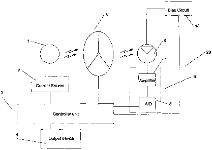
Referring to Figure 1 the light emitter 1 of the present invention generates
radiation of a spectrum coinmensurate with the application. This may be over a
broad range of frequencies including visible and infrared regions of the
electromagnetic spectrum, a broadband signal, or a narrow band signal over a
small
range. Inexpensive emitters such as light emitting diodes, gas discharge lamps
or
tungsten filament lamps are examples. The detector 9 may for example be a
photodiode to detect incident light signals.
The emitter 1 and detector 9 are both controlled by a controller module 3, for
example a microprocessor. Microprocessor 3 includes software, control
algorithms
or coinponent logic to achieve two things.
i) variation in the intensity of light reflected by the sample,
A kqE1~~DW SHEEE
tP~~41A u
CA 02498802 2005-03-11
PCT/NZ2003/000207
Received 16 September 2004
-8-
ii) variation of the spectral response of the detector.
Radiation Source
There are a number of ways of doing both but for siunplicity only a few
examples will be discussed here. For example the inicroprocessor 3 could
control
the intensity of the light einitted from the emitter 1 by varying the current
supply 2.
The operation of the detector 9 is controlled by varying the supply of voltage
or
reverse bias 10. Any signal generated by the detector 9 is ainplified and
converted
into a digital format before being processed by the microprocessor 3.
In another einbodiinent, the light from the emitter 1 is split up into
separate
1o paths before falling incident on the detector 9 seen in Figure 2c. This
operation is
performed by a device called a beam splitter or a chopping wheel 5. The
rotation of
the chopping wheel 5 may be controlled by the microprocessor 3 so that any one
time, the detector 9 will only sense one signal. Typically the chopping wheel
5
blocks the path of other signals while allowing one signal to pass and fall
incident
on the detector 9. The three signals possible in this einbodiinent are the
reference
signal, sainple signal and dark signal (no signal).
Figure 2a illustrates the beain splitting apparatus 30 of the present
invention.
The beam splitting apparatus 30 is comprised of several elements, these
include a
light source 32, a chopping wheel 33, paths to direct the lights 40, 42 and
44, a
2o detector 35, and a sample under test 31. The sample under test is typically
contained by a test tube 31. The test tube 31 may be coinprised of two
diametrically
different sections 31a and 31b. The lower section 31b of this test tube 31 has
a
smaller diameter than the top section 31 a to allow for small amounts of a
sample to
be tested. Alternately a standard test tube may be used, this test tube has a
regular
diameter for its entire lengtll. The test tube 31 containing the sainple is
inserted into
a holding cavity 50 within the spectrophotometer for ineasureinent.
Figure 2b illustrates the reflection angle of the light from the light source
32
towards the chopper wheel 33, along path 44. The angle of reflection is
substantially 90 degrees so that the reflected light, travelling along path
40, is
peipendicular to the detector 35. This allows for optimum information transfer
onto
the light detector 35 with a minimum of diffraction distortion.
AMEN ~~ ~~FET
I P RAVA ~1
CA 02498802 2005-03-11 PCT/NZ2003/000207
Received 16 September 2004
-9-
With reference to Figure 2c, the chopper wheel is comprised of a circular
type barrel with one section of the wheel being substantially flat 34. The
depth of
this flat section 34 is dictated by the diameter of the light transinission
pathways 40,
42 and 44. The depth of the flat section 34 on wheel 33 may be substantially
the
saine as the diameter of the light transinission pathways 40, 42 and 44.
Alternately,
flat section 34 is approximately half way between the circular edge and the
centre of
rotation of the chopper wheel 33.
One coinplete revolution of the chopper wheel 33 will result in any one of
three signals from the detector 35. These tliree signals include a reference
signal, a
1o sainple signal, and a dark signal. The reference signal is when point 33a
on the
chopper wheel 33 is at substantially positive 10 degrees from the vertical
axis. The
infonnation provided at the detector 35 is coming directly from the light
source 32.
The sample signal is detected when point 33b on the chopper wheel 33 is at
substantially at negative 10 degrees from the vertical axis. This infonnation
at the
detector 35 is comprised of the radiation coining from the reflectance off the
sample. At any other tune when there is no light incident on the detector 35
is
known as the dark current. Dark current is important as it provides
information for
the calibration of the spectrophotometer. This infonnation generally relates
to the
temperature drift of the detector 35 and the associated electroiiics.
An alternative embodiment of the physical structure of the spectrophotometer
is shown in Figures 3a to 3c. Referring to Figure 3a, the angle between the
light
source 51 and detector 55 as it reflects off sample 50 is approximately 45 .
The
chopping wheel 56 dictates when the light signal will be incident on the
detector 55.
In Figure 3c, the chopping wheel 53 is divided iiito three sections, namely a
hole
section 62, a miiYor section 60 and a black section 61. The hole section 62
allows
the signal to reflect off the sainple 50 and be detected by the detector 55.
The
mirror section 60 reflects the signal directly to the detector 55. This
results in
reference readings. The black section 61 stops the transinission of light
signal to the
detector 55 so dark current readings may be taken. In this alternative
embodiment,
the chopping wheel 53 is off to one side of the sample 50. This allows
transmission
~~~~~~~~ zdHtFs-
BPEAfIA;)
CA 02498802 2005-03-11
PCT/NZ2003/000207
Received 16 September 2004
-10-
of the signal light through one section of the chopping wheel 53 at any one
time, so
simplifying the control of the chopping whee153.
In a further iinprovement seen in Figures 6 and 7 the chopper wheel 600 may
provide two functions, firstly varying the intensity of the light source
reflected off
the sainple, as well as providing an interinittent direct path to the
detector. This
einbodiinent includes a wheel 600 driven by motor 602 with a nuinber of
apertures
of varying diaineter 704 which allow radiation from the source 606 to reflect
off the
sainple 608 to the detector 610. These match up with apertures 705 in front of
the
detector 610 which don't vary in size. Wheel 600 also includes an axial rim
612
lo which blocks light directly from the source to the detector, except for a
notch 714 to
interinittently allow a direct path between the source and the detector and
block the
sainple for calibration purposes. There are also a nuinber of apertures around
the
periphery 716 and two sensors 718 in the base 620 to allow the inicroprocessor
to
calculate the position of the wheel such that the intensity of the light can
be
recorded alongside the signal received from the einitter. The moving parts are
held
into the base 620 by insert 622. Sample 608 is held in position by spring 624.
In a still further improvement variation of the intensity of the emitter could
be achieved as the light source changes intensity over a veiy short period of
tiine.
For example when a filament is first turned on the amount of light emitted is
not
iminediately at its maxiniuin and takes a finite period of time to increase,
which
depends on the type of filament and the ainbient temperature. In order to
detect
both the intensity of light generated and the consequent signal received by
the
detector different inethods would need to be einployed. For example intensity
of the
light generated could be detected by high resolution section of the voltage
directly
across the filament should give some indication of the change in intensity of
the
radiation generated. Alternatively the source could be pulsed.
Radiation Detector
The detector 35 of the present invention is typically of a pn-junction or a p-
i-
n photodiode type. P-i-n junction photodiodes would provide the fast response
3o necessary if high resolution encoding of incident radiation is required eg
intensity
changes as the source is tuxned on or pulsed. Referring to Figures 4a and 4b,
the
AME~~! ED SMEET
tPF-.A1Ai,l
CA 02498802 2005-03-11
PCT/NZ2003/000207
Received 16 September 2004
-11-
photodetector 35 is connected in reverse bias with a DC voltage source 68, in
particular the negative tenninal is connected to the p-side 65 of the diode 35
and the
positive tenninal is connected to the n-side 67 of the diode 35.
The operation of the detector 35 as it relates to the present invention will
now
be explained. When a photon of light is absorbed by the detector 35 it excites
an
electron and produces a single pair of charge carriers, an electron and a
hole, where
a hole is simply the absence of an electron in the diodes seiniconductor
lattice.
CutTent passes through the semiconductor when the charge carriers separate and
move in opposite directions. The detector 35 collects the photon-induced
charge
lo carriers that can be measured as current or voltage at its electrodes.
An n-type seiniconductor material 67 may be doped with Silicon or
Gennanium to produce an excess of electrons, whereas a p-type material 65 has
an
excess of holes, or an electron deficiency. The area where these two materials
meet
is called the pn-junction. At the pn-junction, tliis disparity creates a
concentration
gradient that causes electrons to diffuse into the p-layer and holes to
diffuse into the
n-layer. This diffusion results in an opposing electrical potential, often
refeired to
as an internal bias. Charge carriers cannot reside in this region, therefore
it is
tenned the depletion region.
In detector 35 of the present invention, light enters the device through a
thin
p-type layer. Absorption causes light intensity to drop exponentially with
penetration depth. Any photons absorbed near the depletion region produce
charge
carriers that are immediately separated and swept across the pn junction by
the
inherent internal bias of the device. Charge carriers created outside the
depletion
region will move randomly, many of them eventually entering the depletion
region
to be swept rapidly across the pn-junction. Some of them will recombine and
disappear without ever reaching the depletion region. This movement of charge
carriers across the pn-junction upsets the electrical balance and produces a
small
photocurrent that is detected at the electrodes of the detector. The
electrical current
or voltage produced is proportional to the light intensity incident on the
detector 35.
Figure 5a, illustrates the response 72 of a typical detector 35 to a varying
intensity 71 for a signal. It can be seen that varying the intensity 71 of the
light
CA 02498802 2005-03-11
PCT/NZ2003/000207
Received 16 September 2004
-12-
source will affect the bandwidth or the total response 73 of the detector 35.
In
particular by increasing the intensity 71 of the light source to high level
91, the
range of wavelengths 73 that can be measured at a particular time is
decreased.
Reducing the intensity 71 of the light source to low level 90 increases the
range of
wavelengths 73 that can be measured but only up to the maxiinuin bandwidth
response of the detector 72.
By increasing the intensity 71 of the light source 1, the Quantuin efficiency
of the detector is increased. The Quantum efficiency is defined as the ratio
of the
photocurrent in electrons to the incident light intensity in photons (or the
sensitivity
lo of the photodetectors to different wavelengths).
Referring to Figure 4a, short wavelengths 80 of light penetrate a short
distance into the structure of the detector 35 ie. light will interact close
to the
surface of the diode. Referring to Figure 4b, longer wavelengtlls 81 of light
penetrate deeper into the structure of the detector 35, or in extreme cases,
the
detector 35 becomes totally transparent to long wavelengths 81. Short
wavelengths
80 of light are coinprised of high energy photons while longer wavelengths 81
contain lower energy photons. The detector 35 only produces a current or
voltage at
its electrodes if the photons absorbed have enough energy or are close enough
to
traverse the pn-junction. This effect is called the `cutoff wavelength'.
Photons with a wavelength less than the cutoff and in close proxiinity with
the pn-junction will produce current or voltage. Photons with a longer
wavelength
greater than the cutoff will not produce cuiTent or voltage.
In order to control the cutoff wavelength it is desirable to control the
thickness of the depletion region 66. One example way to expand this layer 66
is to
apply an external electrical bias (voltage) 68. By applying an external
electrical bias
68, the p-type 65 and n-type 67 regions reduce in thickness so reducing the
efficiency of the longer wavelengths 81 in creating charge carriers. The
thickness
of these layers is directly controlled by the magnitude of external electrical
bias 68.
The greater the magnitude of external electrical bias 68, the thinner the
region where
charge carriers are formed 65 and 67 and the smaller the cutoff wavelength is.
Ideally the control of the voltage 68 is provided by the inicroprocessor 3.
One
~~M~~~~~~ ~~EET
dPF-~q1AU-
CA 02498802 2005-03-11
PCT/NZ2003/000207
Received 16 September 2004
= -13-
skilled in the art will appreciate other ways of varying the spectral response
of the
detector.
Figure 5b illustrates the incorporation of the external bias variable 68 to
aid
in the control of the detector 35. This external bias variable 68 is the
magnitude of
the external voltage 68 applied to the detector 35. As previously discussed,
varying
the voltage 68 varies the thiclmess of the region where charge carriers are
formed 65
and 67 so effecting the response bandwidth of the detector 35. Specifically,
by
increasing the magnitude of the external voltage supply 68, the upper
bandwidth
response of 'the diode decreases 93. The control of extenzal voltage 68 may be
1o controlled by the inicroprocessor 3. Voltage 68 applied to the detector 35
may be
changed in a stepwise manner. Alternately the external voltage 68 is changed
in a
continuous fashion.
By coinbining the control of the light source intensity 71 and the external
voltage applied 68 to the detector 35 by the microcontroller 3, individual
components from the sample signal can be detennined. In practise, for every
stepped change in the external voltage 68, a number of different intensities
71 are
emitted from the light source 1. For every cutoff band selected 70 a new range
of
detectable spectra is observed. The band sweep (due to bias voltage) and
intensity
sweep (due to light source) leads to a combined set of data points arranged
across
the full spectrum of the device under investigation. This way the
characterisation of
all the spectra under investigation is possible.
There are nuinerous possible embodiments in the process of analysing the
spectral absorption of a material in a test sample. In one einbodiment, a
signal, for
example the reference signal, is transinitted through the chopper wheel 33 to
the
detector 35. The controlling module, typically a inicroprocessor 3, selects a
voltage
to be supplied to the detector 35, controlling the width of the depletion
region 66,
and thus selects a predetennined bandwidth that the detector 35 will be
sensitive to.
The microprocessor 3 then varies the voltage supplied to the light source 1
thus
varying the intensity of the broadband light signal. The detector 35 will send
3o representative signals to the microprocessor 3. This data is then stored in
the
microprocessor until the test is fmished. The changes in the level of voltage
AIMEO~~D PHta=j
IPF;1';0
CA 02498802 2005-03-11
PCT/NZ2003/000207
Received 16 September 2004
= -14-
supplied to the detector 35, selects detection bandwidths. This process
repeats until
measurements have been perfonned at all preselected bandwidths. The entire
process is repeated again for.the next light signal, for exainple the light
signal from
the sample path.
In another embodiment of the present invention, one signal, for example the
reference signal, is transmitted through the chopping wheel to the detector.
The
microprocessor selects the predetennined bandwidth that the detector is
sensitive to,
perfonned by selecting the voltage level supplied to the detector. The
inicroprocessor 3 then varies the voltage level supplied to the light source
t11us
lo varying the intensity of the light signal. The detector generates
representative
signals that are transmitted to the inicroprocessor. The chopper wheel then
rotates
and blocks the reference signal and allows the next signal to be transmitted,
for
example the sample signal. Again the microprocessor varies the intensity of
the
light source and the measured values are stored in the microprocessor. As the
1s chopper wheel rotates again there is a dark interval, this is known as the
dark
current. There is no light incident on the detector but an inherent current
will flow
across the pn-junction of the photodiode. This culTent level is measured and
used
by the microprocessor to calibrate for any temperature drift in the
electronics.
The output signals from detector are in the fonn of voltages, these are
20 measured from the detectors tenninals. These signals are representative of
the light
incident on the detectors surface. The output signals are small, they are
proportional
to the amount of current flowing through the diode as a result light being
detected.
These signals are too small and are in the wrong fonnat to be accurately
detected by
the inicroprocessor 3, so they are modified by output circuitry 6. This output
25 circuitry 6 is coinprised of two sections, nainely an ainplification
section 7 and a
conversion section S. The amplification section 7 is coinprised of an
operational
amplifier circuit. The gain provided by this circuit is dependant on the
components
used, therefore gain may be increased or decreased accordingly. Alternately
other
types of amplification circuit 7 may be used in a similar manner. Once the
signal is
3o amplified, it is converted from an analogue signal to a digital signal.
This is
performed either by a dedicated analogue-to-digital converter circuit 8 or in
a
APAZc~~~~~ 11*1HE'~
jFF-,1'1;;j
CA 02498802 2005-03-11
PCT/NZ2003/000207
Received 16 September 2004
-15-
analogue-to-digital converter contained within the microprocessor 3. The
output
signals from the detector are now in a fonnat that the inicroprocessor 3 can
identify
and use.
Signals from the detector are continuously supplied to the inicroprocessor 3
as it is continuously measuring light incident on its surface. The
microprocessor 3
takes discrete measurements froin the continuously supplied signal and stores
these
signals in its inemory.
The output of the detector reflects the presence of material in a sainple.
Once
the test is coinpleted, the inicroprocessor 3 stores the measured values in an
array in
1 o its memory.
Data Analysis
Subsequent evaluation of these measured values may be made by a nuinber
of methods. Some trials and experimentation may be relied upon to determine
the
best method for obtaining values indicative of material presence in a sample.
However, for ease of use, most embodiments will rely upon the comparison of
received measured values with collected or stored data. This data may be
values
which have been pre-programined into the microprocessor 3 so that the
subsequent
collection of iiiitial set-up data by the user may not be required. This
stored data
may comprise of values typical for the type of sainples to be analysed
although it is
2o envisaged for most embodiments that there will be provided provision for
routine
calibration using reference samples either to check accuracy and/or adjust the
apparatus. Calibration information will be stored in the inicroprocessor 3 or
in
software being run by the external processing means. The use of software may
be
more flexible allowing for the updating of software to change the performance
of
the apparatus. In addition, calibration data is updated whenever a new
calibration is
run.
After treatinent of all calibration data with a multiple regression method,
the
correlation factor and the intercept or the free factor are obtained.
Summation of
this fonnula results in typically eight locations in the total calibration
data array.
3o These eight readings relate to the locations that provided the best
measurements.
1~~'~~
CA 02498802 2005-03-11
PCT/NZ2003/000207
Received 16 September 2004
-16-
The spectral response, material size and density is obtained by the
inultiplication of each individual sample reading at the predetermined
position in the
array with its regression coefficient factor and addition of the free factor
as shown
in the following fonnula:
8
Result = free factor +E coefn . measõ
n=1