Note : Les descriptions sont présentées dans la langue officielle dans laquelle elles ont été soumises.
CA 02499568 2005-03-17
WO 2004/027931 PCT/US2003/028849
Description
CURRENT CONTROLLED CONTACT ARC SUPPRESSOR
Technical Field
This invention relates generally to a circuit for
suppression of arcing between two electrical contacts, and more
particularly concerns such a protection circuit Which. makes use
of the current through the contacts to control the arc
suppression circuit, following either the opening or closing of
the electrical contacts.
Background of the Invention
It is a well-known problem that when the flow of
current to an inductive load through a switch or relay contacts
is either interrupted or initiated (such as by opening or
closing and subsequent bouncing of the switch), the energy in
the inductive load is transferred to a voltage spike, which
causes an electrical arc to form between the contacts. This
arcing damages the contact terminals.
There are numerous patents which attempt to remedy or
lessen the effect of the above-described condition. Patent No.
5,703,743 to Lee, which is owned by the assignee of the present
invention; U.S. Patent No. 4,658,320 to Hongel and U.S. Patent
No. 4,438,472 to Woodworth all use an. external "Miller
capacitance" to cause a shunt-connected transistor to turn on
during a high dv/dt event, such as the switch or relay contact
terminals opening. However, these patents all typically operate
during any high dv/dt event, including application of power to
the DC circuit. Usually, this is undesirable.
Other patents include U.S. Patent No. 4,959,746 to
Hongel; U. S . Patent No . 745, 511 to Kugelman et al; U. S . Patent
No. 5,548,461 to James and U.S. Patent No. 5,081,558 to Mahler.
All of these patents use an inductive winding which is coupled
to the primary side of the circuit to turn the shunt transistor
on and off . Kugelman uses an optical. coupler which senses the
current to the relay in order to turn the shunt transistor for
the contacts on and off. James uses an optical sensing device
CA 02499568 2005-03-17
WO 2004/027931 PCT/US2003/028849
2
which turns on when the light from the arc across the contacts
appears. The Mahler patent appears to combine the teaching of
the above patents and the '746 Hongel patent. It uses the
external Miller capacitara.ce to protect the contacts during turn
off (contacts open) and an inductor winding magnetically coupled
to the relay coil to turn the transistor on to protect the
contacts during closing of the contacts. These patents also
will turn on the shunt- protection transistor positioned across
the contact terminals during any high dv/dt event.
Accordingly, a circuit which provides protection
against arcing when the contacts opera. and close, but does not
operate in response to a circuit DC voltage application or other
high dv/dt event when the contacts are open, is desirable.
Summary of the Invention
Accordingly, the present invention is a circuit for
suppression of arcing between electrical contacts, comprising:
a transistor connected. across the contacts; a control c~rcuzt
for controlling the operation of the transistor, wherein turning
on the transistor results in a current path around the contacts,
which tends to prevent arcing between the contacts; and a
current sensor in series with the contacts, wherein when current
is interrupted through the contacts by opening the contacts or
when current occurs through the contacts when the contacts are
just closed, a voltage is produced. which is applied to the
transistor, which maintains the transistor on for a sufficient
time to prevent arcing.
Brief Description of the Drawing
Figure 1 is a block diagram of the system of the
present invention.
Figure 2 is a more detailed schematic drawing of the
system of the present invention. ,
Best Mode for Carrying Out the Invention
In general, the present invention uses an inductance,
in particular, a saturable flyback transformer in the embodiment
shown, and the current therethrough, which is positioned in
CA 02499568 2005-03-17
WO 2004/027931 PCT/US2003/028849
3
series with the contact terminals which are connected to the
load) to control an arc suppression circuit for the contacts.
The flyback transformer stores energy when the
contact terminals are closed. When the terminals open, the
energy in the flyback transformer is transferred to a capacitor
connected to the secondary of the transformer very quickly in a
flyback action. The voltage on the capacitor is used to power a
switch control circuit, which assists in turning the protection
transistor connected across the contacts on and maintaining it
on. A small amount of additional "Miller capacitance" is used
to help turn on the protection transistor faster than otheravise.
Generally, this invention may be used with all kinds of shunt
(by-pass) transistors. The basic electrical circuit which
controls the protection transistor is also well known. The,
energy from the secondary circuit, stored in the flyback
transformer when it is in a saturated condition, provides the
energy to drive the protection (by-pass) transistor or other
high-speed switching device when the contacts open or dose.
As indicated above, the present invention includes a
transistor which forms a by-pass (shunt) around the switch or
relay contacts for current, preventing damage due to arcing,
which is particularly useful when the load is inductive. The
present invention protects against arcing, both in the opening
and closing of the protected contacts, as well as preventing the
protection transistor from turning on when the contacts are open
and the DC circuit feeding~the protected contacts is energized,
or other high dv/dt events. It is undesirable to have the
protective transisrtor turn on in response to such high dv/dt
events when the contacts are open.
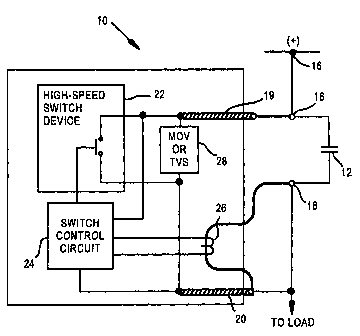
Figure 1 shows a block diagram of the protection
circuit of the present invention, shown generally at 10. The
circuit protects contact terminals 22, which are connected at
one side 14 to the positive side 16 of a DC supply, with the
other side 18 connected to the negative side of the supply and
the load. The two sides 14, 18 of the contacts 12 are connected
to terminal posts or blocks 19 and 20, respectively, which are
the physical connections to the protection circuit 10. The
protection circuit 10 operates by briefly by-passing or shunting
CA 02499568 2005-03-17
WO 2004/027931 PCT/US2003/028849
4
current produced by the inductive load around the contact
terminals 12 through a high-speed switching device 22, which is
typically a transistor or similar device, during opening or
closing of contacts 12. Switching device 22 is controlled by a
control circuit 24, which operates in response to voltage
developed across the protected contacts 12 and current through
an inductor 26, typically a flyback transformer, during opening
and closing of the contacts. The current stored in flyback
transformer 26 provides the energy to operate control circuit
24.
Briefly, when contacts 12 close, high-speed. sc~itch
device 22 is turned on for a very short time to protect contact
terminals 12 from arcing when the terminals bounce following
initial contact. Further, when contacts 12 open, high-speed
switch 22 is turned on to prevent an.arc from forming during the
separation of the contacts, remaining on long enough for the
contact terminals to separate sufficiently to withstand
substantial voltage (several hundred volts) without arcing. The
high-speed switch then turns off and a transient voltage
suppressor, in particular metal oxide varistor (MOV) 28 or other
similar equivalent device, will clamp the flyback voltage to
several hundred volts and dissipate the energy stored in the
inductive load in the form of heat.
When contacts 12 are open, and there is no current
flowing through the contacts, the switch control circuit 24 will
not operate to protect the contacts, i . e. will not turn on the
high-speed switch device for longer than a negligible period of
time. The high-speed switch thus is prevented from turning on
in response to the DC circuit for the protected contacts being
energized, avoiding temporary load energization for such high
dv/dt events. .
One important aspect of the present invention is the
use of the inductor (flyback transformer) 26 and the current
therethrough to turn on. the high-speed switch following both the
opening and the closing of contacts 12. The flyback transformer
26 is on the secondary, i.e. load side, of the relay (with
protected contacts 12).
CA 02499568 2005-03-17
WO 2004/027931 PCT/US2003/028849
In the circuit of Figure 1, the high-speed switch 22
can be any one of various transistors, and the contacts, again,
can be any one of various switch and/or relay contact
arrangements, including magnetic, manual, optical or other types
5 of contacts.
Referring now to Figure 2, which shows one specific
implementation of the circuit of the present invention.
Terminal posts 40 and 42 correspond to terminal blocks 19 and 20
in Figure 1. The protected contacts 43 correspond to protected
contacts 12 in Figure 1.
When the protected. contacts 43 are closed (and are
now to be opened), and a load current is flowing through them,
such as approximately 800 mA or greater, the current through the
protected contacts 43 is also applied through the primary or
center winding of a toroidal inductor (flyback transformer) 44.
The transformer will be saturated under normal conditions with
the above current when contacts 43 are closed. When the
contacts are opened, presenting the possibility of an arc, the
voltage across the contacts will begin to rise due to the LRC,
circuit formed by the inductance, series resistance and
parasitic winding capacitance associated with the load.
When this voltage reaches the threshold rating of
high-speed switching transistor 48, which in the embodiment
shown is an IGBT transistor, a current will begin to flow from
the collector (positive terminal? of transistor 48 into its
gate, through capacitor 50. This results in transistor 48
quickly turning on, which will prevent the voltage across
contacts 43 from further increasing. Transistor 48 will remain
in a linear operating mode for a brief time, with a contact
voltage of about 8-12 volts and an dv/dt of about 20 volts per
millisecond. Capacitor 52 prevents the collector voltage from
transistor 48 turning transistor 54 on through capacitor 56 and
resistances 72 and 60. Transistor 54 in the embodiment shown is
a MOSFET transistor and is part of the control circuit for
transistor 48.
In addition, when the contacts 43 open, the current
through inductor 44 (the primary of the flyback transformer) is
interrupted, which results in a collapse of the magnetic field
CA 02499568 2005-03-17
WO 2004/027931 PCT/US2003/028849
6
sustained by that current. This causes the voltage in the
secondary of the transformer to increase rapidly. That
secondary voltage is applied to a full wave rectifier comprising
diodes 64-67, Which is used to heavily charge the gate of
transistor 48 and capacitor 50. In a relatively short time
(1-1.2 microseconds), transistor 48 is driven into saturation and
capacitor 50 is charged to 15 volts, the value of which is
limited by zener diode 70, because of its breakdown voltage of
volts. Resistors 60 and 72 keep the gate voltage of
10 transistor 54 below its minimum rated threshold voltage, as long
as the collector of transistor 48 is below its maximum
saturation voltage.
After all of the energy stored in transformer 44 has
been dissipated to capacitor 50, transistor 48 and zener diode
15 70, capacitor 50 will begin to discharge through resistor 74.
Transistor 48 will remain in saturation until its gate voltage
decays to its threshold value, which takes about 1.2
milliseconds. When the gate voltage reaches that threshold.,
transistor 48 begins to turn off and capacitor 50 will conduct,
keeping transistor 48 turned on in a linear mode, with an
increasing dv/dt of approximately 16 volts/ms. As the voltage
increases, the gate voltage of the transistor 54 will begin to
increase as well. In about 300-500 microseconds, the gate
voltage of transistor 54 will reach its threshold voltage and
will begin to conduct, charging capacitor 56 and turning
transistor 48 off very quickly. As transistor 48 turns off, its
collector voltage, which is increasing, turns transistor 54 on
harder, which in turn turns transistor 48 off harder, in a
cyclical manner.
Accordingly, transistor 48 will protect the contact
terminals 43 by shunting the load current around the contact
terminals for a period of 3-4 milliseconds, which alloWS the
contact terminals 43 to separate sufficiently that they can
withstand several hundred volts without arcing. The collector
voltage of transistor 48 will continue to rise at a rate of
about 60-85 volts per microsecond, until it reaches the clamping
voltage of the metal oxide varistor (MOV) 76, which is typically
several hundred volts. At this point, the current through
CA 02499568 2005-03-17
WO 2004/027931 PCT/US2003/028849
7
transistor 48 is transferred to MOV 76. MOV 76 dissipates the
energy from the external inductance as heat, and the load
current goes down to zero. When the current through the load
reaches zero, the voltage across MOV 76, protecting transistor
44 and contacts 43, will return to the open circuit voltage of
the protected contacts 43.
When the contacts are closed, after being open, there
is a risk of arcing as the contacts again open slightly for a
very short period of time, which is referred to as contact
"bounce". In this mode, capacitor 56 will discharge through
contacts 43, resistance 78 and diode 80. The peak discharge
current is limited by resistor 78, which reduces the effect of
the current on diode 80.
Likewise, capacitor 50 discharges through parallel
discharge paths of zener diode 70, which is current-limited by
resistor 84 and the internal diode of transistor 54, which is
current-limited by resistor 58. This current limitation by the
resistors improves the life of the circuit as a avhole.
Current increases through the primary of flyback
transformer 44 following closing of the contacts 43, because
current is now flowing through the protective contacts,
resulting in a voltage in the secondary winding of the flyback
transformer, which in turn charges the gate of transistor 48 and
also begins to charge capacitor 50. This voltage is limited to
2S 15 volts by the zener diode 70. Transistor 48 is driven into
saturation, providing a current by-pass (shunt) path and
protecting the contact terminals from arcing during bouncing at
closing of the contacts.
Capacitor 50 will be discharged by resistor 74 in
approximately 3-4 milliseconds after the contacts close, causing
transistor 48 to turn off. The current through. the primary of
flyback transformer 26 will. eventually cause the transformer to
saturate; the circuit is then in a state to protect the contact
terminals when they open, as explained above.
When the contacts 43 are fully open, but the voltage
across the contacts is zero, the current through the flyback
transformer 26 will be zero and no energy will be stored in the
transformer. When the contact terminals are connected across a
CA 02499568 2005-03-17
WO 2004/027931 PCT/US2003/028849
8
DC voltage, the contact voltage, as indicated above, will
increase rapidly; when it reaches the threshold voltage rating
of the IGBT transformer 48, a current will begin to flow from
the positive contact terminal (or the collector) of transistor
48 through capacitor 50 and into the gate of transistor 48, as
explained above. In a short time, transistor 48 will turn on
and prevent the contact voltage from increasing any further.
Transistor 48 will remain in linear mode with a
contact voltage of about 8-12 volts and a dv/dt rate of about 20
volts/ms, which results in a "let-through" current to the load.
Since there is no stored ez~.ergy in the flyback transformer,
however, to further turn on the transistor 48, the transistor 48
will remain at 8-12 volts and capacitor 52 will continue to
charge through capacitor 56 and resistors 60 and 72. When
capacitor 52 charges to the threshold voltage of transistor 54,
it will begin to conduct, charging capacitor 50 and turning
transistor 48 off very quickly. As transistor 48 turns off, its
increasing co33ector vo3tage turns on transistor 54, which in
turn turns transistor 48 off harder. Capacitor 52 and resistors
60 and 72 are designed to charge to the threshold voltage in
about 30-95 microseconds. The duration of the let-through
current is thereby limited to less than 95 microseconds,
virtually eliminating the problem of previous circuits where the
high-speed switch would operate in response to the DC circuit
being energized.
Capacitor 56, in addition, to the above function, is
designed to AC couple the turn-on circuit for transistor 54,
which comprises resistors 60, 72 and capacitor 52. By AC
coupling the turn-on circuit for transistor 54, the DC leakage
current from the positive terminal to the negative terminal is
significantly reduced. During transient operations, capacitor
56 appears as a short circuit. Diode 86 is provided to protect
the device from polarity reversals. such as occurs when the
terminals axe connected backwards. A zener diode 90 is provided
to protect the transient voltages from damaging transistor 54.
Accordingly, a circuit has been disclosed which
protects electrical contacts from arcing, both during opening
and closing of terminals. It makes use of an inductive element
CA 02499568 2005-03-17
WO 2004/027931 PCT/US2003/028849
9
operating off the secondary (load) side current of the contacts
to control the operation of a high-speed transistor, such as an
IGBT, which by-passes (shunts) current around the contacts for
specific times to prevent arcing. In addition, the invention
limits the time the resulting current due to circuit
energization and other high dv/dt events is allowed to flow
through the load to less than about 95 microseconds.
Although a preferred embodiment of the invention has
been described for purposes of illustration, it should be
understood that various changes, modification and substitutions
may be incorporated in the embodiment without departing from the
spirit of the invention which is defined in the claims which
follow.
What is claimed is: