Note : Les descriptions sont présentées dans la langue officielle dans laquelle elles ont été soumises.
CA 02502841 2005-04-18
WO 2004/040898 PCT/US2003/033709
SYSTEM AND METHOD FOR SUPPRESSING NOISE
IN A PHASE-LOCKED LOOP CIRCUIT
BACKGROUND OF THE INVENTION
1. Field of the Invention.
This invention relates to generating frequency signals in a signal processing
system,
2. Description of the Related Art,
Phase-Locked Loop (PLL) circuits have been used in many wireline and wireless
applications for generating carrier frequencies and timing reference signals.
Fig. 1(a) shows a PLL which is commonly used in a communications transceiver.
This
circuit includes a phase and frequency detector 1, a loop filter 2, and a
voltage-controlled,oscillator
3 which outputs a signal fo~t at a desired frequency. A feedback loop
connecting the oscillator to
an input of the phase and frequency detector includes a divider 4 which
divides the output of the
oscillator by a value of (N + 9 )IN. A modulus control circuit outputs a
signal to the divider for
controlling the value of N.
In a PLL of the aforementioned type, it is well known that a trade-off exists
between loop
bandwidth and channel spacing. It is also known that channel spacing is the
same as the
comparison frequency. Given this relationship, it is often desirable to set
the loop bandwidth of the
PLL to be smaller than the comparison frequency by a factor of ten. Reducing
the loop bandwidth
to this value, however, produces a number of drawbacks.
For example, loop bandwidth not only affects channel spacing, it also affects
the lock time
and amount of phase noise in a PLL. In fact, loop bandwidth is inversely
proportional to both of
these values. Therefore, reducing the loop bandwidth to a value smaller than
the comparison
frequency by a factor of ten will produce a commensurate increase in phase
noise and lock time,
which has found to be undesirable for many applications.
Anotherdrawback of the aforementioned PLL relates to a second type of noise.
This noise
appears in the form of spurious signals generated from mismatches that occur,
for example, from
the charge pump and the phase and frequency detector. More specifically, as
shown in Fig.1 (b),
one mismatch occurs between the UP and DOWN current (or more accurately the
current sources)
of the charge pump. Another mismatch occurs between the UP and DOWN signal
paths in the
phase and frequency detector, where ideally no mismatch should exist. These
mismatches
CA 02502841 2005-04-18
WO 2004/040898 PCT/US2003/033709
generate spurious signals which propagate throughout the host system to
degrade performance
and therefore, like phase noise, are also considered to be undesirable.
Fig. 2 shows the manner in which these spurious signals are formed. In this
diagram, for
corresponds to the output frequency of the phase-locked loop and f~~to,~
corresponds to the cutoff
frequency of the PLL loop filter. The difference between fat and f~~ro,~
defines the loop bandwidth
of the circuit. In operation, mismatches along the signal path of the loop
generate one or more
spurious signals fsP that are located very close to the output frequency foUt.
In fact, the spurious
signals are so close to the output frequency (Of is very small) that they lie
within the loop
bandwidth of the circuit and therefore cannot be removed by the loop filter.
These unsuppressed
spurious signals furthercontribute to the degradation of signal quality and
performance ofthe host
system.
In view of the foregoing discussion, it is evident that there is a need for a
system and
method for effectively suppressing noise in phase-locked loop circuits and
especially loop circuits
that are used in host systems having low noise and lock-time requirements.
SUMMARY OF THE INVENTION
An object of the present invention to provide a system and method for
effectively
suppressing noise in a phase-locked loop circuit.
Another object of the present invention is to provide a system and method for
suppressing
at least two types of noise in a phase-locked loop, namely phase noise and
spurious noise
generated from mismatches that exist along the loop circuit signal path.
Another object of the present invention is to provide a system and method
which achieves
one or more of the aforementioned objects without placing any restrictions on
loop bandwidth,
operating frequency, or any other functional parameter of the phase-locked
loop.
Another object of the present invention is to provide a system and method
which achieves
one or more of the aforementioned objects while simultaneously reducing the
lock time of the
phase-locked loop.
Another object of the present invention is to suppress at least one of the
aforementioned
types of noise using a loop filter of the phase-locked loop.
Another object of the present invention is to achieve one or more of the
aforementioned
objects for a phase-locked loop controlled by a Sigma-Delta modulator.
CA 02502841 2005-04-18
WO 2004/040898 PCT/US2003/033709
Another object of the present invention is to provide a control system which
achieves one
or more of the aforementioned objects and also modulates a reference signal
forthe phase-locked
loop in a way that finely adjusts the resolution of spurious noise
suppression.
These and other objects and advantages of the present invention are achieved
by
providing a system and method which suppress noise from the output of a
frequency generator
such as a phase-locked loop. This is accomplished using a modulation scheme
which shifts
spurious noise signals outside the loop bandwidth of the generator. When
shifted in this manner,
the noise signals may be removed entirely or to any desired degree using, for
example, a standard
filter located along the signal path of the generator. As a result, the signal-
to-noise ratio of the
generator is substantially improved, loop bandwidth may be increasd, and
faster lock times may
be realized.
In accordance with one embodiment, the present invention provides a noise
supression
method that generates a frequency signal from a phase-locked loop based on a
reference signal
and then removes noise from the frequency signal by shifting a spurious signal
of a predetermined
order outside a loop bandwidth of the PLL. The loop bandwidth may be defined
by a cutoff
frequency of a loop filter, or alternatively by a frequency range lying
between an output frequency
and cutoff frequency of the filter. To achieve complete noise suppression,
first-order spurious
signals are shifted outside the loop bandwidth. However, suppression of only
higher-order signals
may be performed if application requirements so require or if otherwise
desired.
The spurious noise signals are shifted by controlling the value of a pulse-
swallow divider
situated along a feedback path of the phase-locked loop. The value of this
divider may be
controlled by a Sigma-Delta modulator and more specifically the modulation
ratio set within this
circuit. The noise being suppressed includes at least one of phase noise and
noise generated by
mismatches that occur in the phase and frequency detector andlor the charge
pump of the PLL.
In accordance with another embodiment, the present invention provides a method
for
suppressing noise by modulating a reference signal and then generating a
frequency signal from
a phase-locked loop based on the modulated reference signal. The modulation is
performed to
ensure that harmonics of the original reference signal and the modulated
reference signal are not
coincident, at least throughout a significant range of frequencies.
Preferably, the modulated
reference signal is used to generate the PLL frequency signal only during
times when the
harmonics are not coincident. This method may be used to provide fine
adjustments to the
spurious noise suppression performed by the Sigma-Delta modulator discussed
herein.
-3-
CA 02502841 2005-04-18
WO 2004/040898 PCT/US2003/033709
In accordance with another embodiment, the present invention provides a
frequency
generator which includes a phase-locked loop that generates a frequency signal
based on a
reference signal and a noise suppressor which shifts a spurious signal of a
predetermined order
outside a loop bandwidth of the PLL. The phase-locked loop includes a loop
filter, and the loop
bandwidth is defined by a cutoff frequency of the loop filter or corresponds
to a frequency range
that lies between the frequency signal generated from the PLL and a cutoff
frequency of the filter.
The noise suppressor preferably includes a frequency divider in a feedback
loop of the PLL and
a controller which sets the frequency divider to a value which performs the
spurious signal shift.
The frequency divider may be a pulse-swallow divider and the controller may
include a Sigma-
Delta modulator. In addition to these features, the noise suppressor may
include a reference
signal modulator for fine tuning suppression of the spurious signals.
In accordance with another embodiment, the present invention provides a system
for
controlling a phase-locked loop comprising a divider which divides a frequency
signal output from
the PLL and a controller which sets the divider to a value which shifts a
spurious noise signal of
a predetermined order outside the loop bandwidth of the PLL. The loop
bandwidth may be defined
based on the cutoff frequency of a loop filter and the divider value may be
controlled to suppress
virtually any order of spurious noise signals desired. The controller may also
include a modulator
for generating a modulated reference signal for fine tuning supression of the
spurious signals.
BRIEF DESCRIPTION OF THE DRAWINGS
Fig.1 (a) is a diagram showing a related-art phase-locked loop circuit, and
Fig. 1 (b) is a
diagram showing different types of mismatches that may occur in the phase and
frequency
detector andlor charge pump of the related-art phase-locked loop, which
mismatches lead to the
generation of spurious signals that degrade system performance.
Fig. 2 is a diagram showing the generation of a spurious noise signal in the
related-art
circuit of Fig.1 (a).
Fig. 3 is a diagram showing one embodiment of a phase-locked loop circuit in
accordance
with the present invention.
Fig. 4 is a diagram showing an example of how the system and method of the
present
invention may be implemented to shift spurious noise signals outside the loop
bandwidth of a PLL
to thereby enable them to be removed by a loop filter.
-4-
CA 02502841 2005-04-18
WO 2004/040898 PCT/US2003/033709
Figs. 5(a) and 5(b) are graphs showing harmonics of an original reference
frequency and
a modulated reference frequency generated in accordance with one example of
the present
invention.
Fig. 6 is a diagram showing one embodiment of the reference modulator of the
present
invention.
Fig. 7 is a diagram showing another embodiment of the reference modulator of
the
present invention.
Figs. 8(a) - 8(g) are diagrams showing the manner in which signals are
processed by each
of the elements of the reference modulator shown in Fig. 7.
Fig. 9 is a diagram showing one embodiment of the reference modulator of the
present
invention.
DESCRIPTION OF THE PREFERRED EMBODIMENTS
The present invention includes various embodiments of a system and method for
suppressing noise in a phase-locked loop circuit. In accordance with one
embodiment, the system
and method suppresses noise that results from mismatches relating to the
charge pump and
phase and frequency detector. This is accomplished using a Sigma-Delta
modulator which
controls a divider in a feedback path of the PLL so that spurious noise
components are shifted
outside the operating loop bandwidth of the circuit. Other embodiments
suppress noise by
modulating a reference frequency signal input into the phase and frequency and
detector. Still
other embodiments suppress noise using a combination of the foregoing
techniques. Through
these embodiments, spurious noise components are shifted far away from the
desired output
frequency of the PLL so that they can be eliminated by a loop filter. As a
result, a substantial
improvement in signal-to-noise ratio and loop bandwidth may be realized along
with a proportional
reduction in phase noise and lock time.
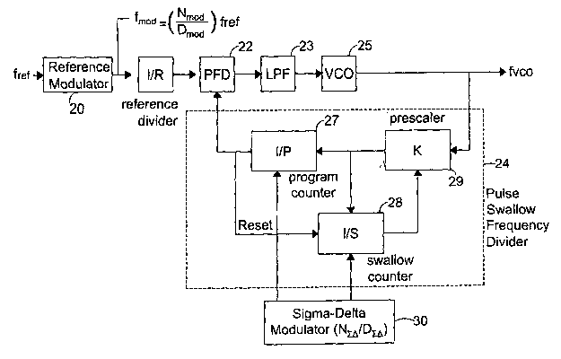
Referring to Fig. 3, one embodiment of the system and method of the present
invention
includes a reference modulator 20 and a Sigma-Delta modulator 30 for
controlling the output
frequency of a phase-locked loop. The phase-locked loop is formed from a phase
and frequency
detector 22, a loop filter (e.g., a low-pass or bandpass filter) 23, a pulse-
swallow frequency divider
24, and a voltage-controlled oscillator 25 for outputting a signal at a
desired frequency f~~o. The
pulse-swallow frequency divider includes a program counter 27 and swallow
counter 28 which
respectively assume values P and S under control of the Sigma-Delta modulator.
-5-
CA 02502841 2005-04-18
WO 2004/040898 PCT/US2003/033709
The Sigma-Delta modulator sets the values of the program and swallow counters
based
on parameters, N~o and Duo, in order to generate the desired output frequency
f~~o. This output
signal may be used to modulate or demodulate signals in a communication
transceiver or to
perform any one of a variety of other purposes. The values of P, S, N~o and
Duo may be
determined from the specific prescaler being used. Various prescalers and the
manner in which
they may be used to set the values of the counters are generally known to
those skilled in the art.
See, for example, the text RF MICROELECTRONICS, Chapter 8, by Behzad Razavi.
If left uncorrected, the output frequency of the voltage-controlled oscillator
will contain
various types of noise, including spurious signals generated from mismatches
relating to the phase
and frequency detector and the charge pump. This situation is depicted in Fig.
2 where the
frequency separation ~f is so small that the spurious signals cannot be
removed by the loop filter.
The present invention removes this and other types of noise (including phase
noise) by shifting
the spurious signals far away from the output frequency f~~o of the PLL. This
is accomplished
through adjustments made by the Sigma-Delta modulator, which adjustments are
preferably
performed in combination with a modulation of the reference signal of the PLL.
First, the reference modulatormodulates the input reference signal f~efby an
amountwhich
causes this signal to be multiplied by the value Nmod , This results in the
formation of a modulated
~moa
reference signal, fmoa- frer * Nmod , which is input into the phase and
frequency detector. To effect
Dmod
this modulation, the values of Nmod and Dmoa are preferably selected to be
integers by observing
one or more of the following considerations:
1 ) The frequency range of the system. If the required frequency range is very
narrow
and only a few channels exist in the range, only one reference modulator may
be used. However,
if the range is very wide, one reference modulator may not be sufficient to
achieve a desired
degree of spurious signal suppression. In this case, multiple reference
modulators may be
included and selectively chosen to achieve an optimal degree of suppression.
Tables 2 and 3
(discussed in greaterdetail infra) include non-limiting example of the values
of Nmod and Dmod which
may be used to perform the reference signal modulation of the present
invention. If the required
frequency range does not include the frequency of 944.65 MHz or 1102.1 MHz,
8l9 modulation
may be enough for suppression. But, if that frequency is included another
modulation such as 516
-6-
CA 02502841 2005-04-18
WO 2004/040898 PCT/US2003/033709
may be used for the applicable channel. This multiple reference-modulator
embodiment is
discussed in greater detail below.
2) The desired spur level for the system.
3) The loop filter bandwidth, which may be explained as follows. The
parameters of
the loop filter depend on the reference frequency. As the reference modulation
changes the
reference clock, the loop filter parameters should be changed. If the
difference between the
original reference clock and the modulated reference clock is small, the loop
filter can be shared
for both the original clock and the modulated clock as long as system
specifications such as phase
noise, spurious signal suppression, and lock time allows it. For example, if
819 modulation and 213
modulation for a channel shows the same spurious signal suppression, the 8l9
modulation may
be preferred because the 8I9 modulated reference signal is closer to the
original reference
frequency than the 213 modulated reference signal.
4) The hardware complexity of the system. For example, while multiple
modulation
ratios (314, 516, 718, 819, etc.) may be acceptable for purposes of achieving
a desired level of
spurious signal suppression, it may not be possible to achieve all the ratios
given the hardware
in use. Thus, hardware may be one factor to consider when selecting a
modulation ratio in
accordance with the present invention.
During the time the reference signal is modulated or some predetermined time
before, the
values defining the modulation ratio of the Sigma-Delta modulator, N~o and
Duo, are computed
along with P and S which correspond to the values of the program and swallow
counters.
Together, these parameters along with parameter K of prescaler 29 determine
the value the pulse-
swallow frequency divider uses to divide the output frequency of the VCO. One
way in which
parameters N~o, Duo, P, and S may be calculated will now be discussed in
greater detail.
The values of f~~o, R, K, and fe, are preferably determined at the system or
architecture
level to meet, for example, the requirements of a desired application. (The R
value may be related
to the design specification of the PLL (e.g., R = 1 if fef = 19.2 MHz) and the
K value may be
related to the design of the prescaler.) The only unknown values therefore are
P, S, N~o, and Duo.
Duo. This parameter may be determined in various ways. First, Duo may be
determined
as a simple poweroftwo, e.g., 2'~I21~~2'3 . . . In this case, as the
denominator increases, hardware
complexity also increases and the frequency resolution of the PLL increases.
Thus, there is a
trade off between precision and hardware complexity. Second, if the frequency
resolution (or
channel spacing) of the system is known, Duo may be determined by the
following equation:
CA 02502841 2005-04-18
WO 2004/040898 PCT/US2003/033709
Duo = (frets R) ~ f~~. For example, in the Korean CDMA system, fe,-19.2 MHz, R
=1, and f~h =10
kHz. Given these values, Duo =1920.
P. S, and N~o. These parameters are integer values which satisfy the following
relation:
f~~o - (fret/ R) x (K P + S + N~ol Duo). If two or more constraints are added
to this relation, the
solution is unique. The first constraint is that 0 <_ S < K and the second
constraint is that 0 _< N~o
< Duo. Actually, these constraints are not algorithmic but practical ones.
Because the range of N~o
exceeds Duo for many applications, the hardware complexity of the Sigma-Delta
modulator
increases accordingly. For example, assume that f~f=19.2 MHz, R =1, f~~o
=1920.192 MHz, K
= 8, and Duo =19200. Then, the term (KP + S + N~ol Duo) =100.01, where KP + S
= 100 and
N~o/ Duo = .01 as K, P and S are all integer values. Thus, P =12 and S = 4
(the constraint S < K
makes this integer solution unique) and N~o =192.
Second, the pulse-swallow frequency divider divides the output of the voltage-
controlled
oscillator f~~o by the value in Equation (1), so that the comparison frequency
input into the phase
and frequency detector equals the modulated reference frequency, fmod = Dmod
f~ef~
mod
(r~~ p + s) + ( N~~ ) (1 )
DEe
Since the modulated reference frequency f~,od is different from the
unmodulated reference
frequency f~e,, the parameters of the pulse-swallow frequency divider must be
changed so that the
signal input into the phase and frequency detector from the feedback loop
matches the modulated
reference frequency output from the reference modulator. Before being input
into the phase and
frequency detector, the modulated reference frequency f",od may be divided by
the value R
corresponding to an optional reference divider 31.
From Equation (1 ), it is clear that in order to achieve a desired output
frequency signal f~~o
(which, for example, may be a local oscillator signal used in baseband signal
recovery circuit of
a communications transceiver), the output of the voltage-controlled oscillator
must be divided by
a value given by Equation (1 ) in the feedback loop. If the reference divider
and prescaler counter
values R and K are known for a given application, the remaining parameters (P,
S, N) can be
determined as explained above and in view of Equation (1) for a given input
frequency and the
VCO output frequency.
_$_
CA 02502841 2005-04-18
WO 2004/040898 PCT/US2003/033709
The output frequency of the PLL may be expressed by the following equation:
ao ~ Ref ) ~ Dmod~ ( ~K~ p ~- S) + ~ DE° ~~
In Equation (2), the term ~ f ef ) ~ N mod (K ~ p + s) represents the integer
part of the
R D mod
desired frequency f~~o and the term C Ref ~ C D modl C D~° ~ represents
the fractional part
of this frequency. When mismatches occur in the PLL, spurious noise signals
form at
frequencies which coincide with the fractional part of the desired frequency
f~~o 'and
harmonics of this frequency. In order to achieve the separation required to
filter out all or
a portion of these spurious signals, the present invention controls one or
more parameters
in the above equation.
Initially, the modulation ratio of the Sigma-Delta modulator is controlled to
achieve
a desired degree of frequency separation. This may be empirically understood
with
reference to the fractional part of Equation (2), which corresponds to the
frequency offset
(Of) between the desired frequency f~~o and the first-order spurious signals
fsp~. (This offset
may also exist between adjacent-orders of the spurious signals themselves.)
As the modulation ratio N~° of the ,,Sigma-Delta modulator
increases, the
DE°
frequency offset (or separation distance between the spurious signals and the
desired
output frequency) becomes larger. Inclusion of the term N~° in the
fractional part of
DE°
Equation (2) thus ensures that spurious signals fsp of a predetermined order
are formed
sufficiently far from the desired output frequency f~~o that they can be
removed by loop filter
23 along the signal path. This may be achieved, for example, by making the
fractional part
in Equation (2) and more specifically the ratio of N~o and Duo relatively
large. This affects
-9-
CA 02502841 2005-04-18
WO 2004/040898 PCT/US2003/033709
the values of P and S which, in turn, ultimately leads to an adjustment of the
value of the
pulse-swallow feedback divider of the PLL.
To achieve complete noise supression, the fractional part of Equation (2) is
set
large enough to ensure that the first-order spurious signals are shifted below
the cutoff
frequency of the loop filter. If desired, however, the fractional part may be
set to other
proper values to filter out higher-order spurious signals. While a lesser
degree of noise
suppression is realized in this case, other system requirements may be met,
thereby making
the present invention a suitable solution.
Fig. 4 shows how adjusting the values of N~o and Duo can lead to suppression
of
spurious noise signals in the output of the PLL. In this illustrative example,
f~CO corresponds
to the desired output frequency of the PLL, f~,~o,~corresponds to the cutoff
frequency of the
loop filter, and the loop bandwidth corresponds to the difference between f~~o
and f~~to,~. In
accordance with the present invention, the fractional part of Equation (2) and
particularly the
ratio of N~o and Duo is computed to be sufficiently large to shift the
spurious noise signals
fsp,, fsPa, . . fSpN outside the loop bandwidth and thus in this case below
cutoff frequency f~~toff
where they can be removed by the loop filter. This shift is shown by frequency
offset Of.
The ratio of Nmoa and Dmod of reference modulator 20 may be controlled to
further
adjust the degree of separation. More specifically, while this reference
modulator is
considered to be an optional feature of the present invention (e.g., the
frequency separation
required for spurious noise suppression may be accomplished solely by
adjusting the
modulation ratio formed between N~o and Duo), the ratio of Nmod and Dmod may
be controlled
as a way of fine tuning the spurious signal shift performed in the fractional
part of Equation
(2). The values of Nmod and Dmod are preferably determined based on the design
of the
reference modulator.
Table 1 provides examples of values which when input into Equation (2)
generate
a frequency separation ~f sufficient to shift spurious noise signals outside
the loop
bandwidth of the PLL. These values are reflected in Fig. 4 to illustrate the
superior
performance of the invention.
905.29MHz 19.68MHz 1 8 9 4 ~ 12 ~ 3 ~ 11817 ~ 15744
-10-
CA 02502841 2005-04-18
WO 2004/040898 PCT/US2003/033709
Table 1
In Table 1, NFO and Duo values are set to 11817 and 15744 respectively and the
modulation ratio of the reference signal modulator is 819. Plugging these
values into
Equation (2), the output frequency f~~o of the PLL is calculated to be 905.29
MHz. The value
corresponding to the fractional part of this equation reveals the superior
performance of the
present invention for this example:
Nm~a N~° 19.68 . $ , 11817 - 13.13 MHz (3)
9 15744
As shown by Equation (3), spurious noise signals produced from mismatches in
the
PLL will appear at frequencies which coincide with the fractional part of
Equation (2), which
is computed to be 13.13 MHz. The frequency separation ~f between the output
frequency
and the first-order spurious noise signal fsp~ will therefore be 6.55 MHz.
(This number is
obtained by subtracting 13.13 MHz from the frequency of the modulated input
reference
signal (19.68 * 8l9)). Using these values, the Sigma-Delta modulator shifts
the first-order
spurious signals outside the loop bandwidth of the PLL, thereby allowing the
cutoff
frequency f~~to" of the loop filter to eliminate these and higher-order noise
signals from the
output frequency. While the modulation ratio of 819 is used in this example
and provides for
fine resolution adjustment, it can be seen that an even wider frequency
separation may be
achieved with other reference modulating ratios.
In the foregoing example, the cutoff frequency and/or the loop bandwidth may
be
determined based on the specific application requirements of the system
including
requirements for phase noise and spurious signal suppression. As shown, a
greater
suppression of the spurious signal fsP occurs by the loop filter as the
frequency offset (~f)
increases from the carrier f~~o increases. While optional, the reference
modulation may
advantageously be used to increase this frequency offset.
Also, in the foregoing example, the frequency separation was achieved at least
in
part by setting the modulation ratio of the Sigma-Delta modulator to a
relatively large value.
For comparison purposes, it is noted that a small value of this ratio would
not be able to
achieve the separation required for noise suppression. For example, if the
N~° _ 111968
DE°
-11-
CA 02502841 2005-04-18
WO 2004/040898 PCT/US2003/033709
and the P and S values are 11 and 2 respectively, then the resulting frequency
separation
would be~ 10 kHz for the same values of K and f~ef using an umodulated
reference frequency.
This separation would in most applications lie well within the loop bandwidth
of the PLL and
thus would not be able to be suppressed by the loop filter.
Additionally or alternatively, in controlling the values of the Sigma-Delta
modulator
the numerator N~o may be' adjusted to be far away from the sub-harmonics of
the
denominator Duo. This means, for example, that if the ratio of the numerator
and
denominator N~° of the Sigma-Delta modulator is near Dxo 12, D~ol4, and
D~ol 8, the
D~°
reference modulation can reduce or eliminate the spurious signals.
The present invention thus effectively suppresses noise in a frequency
generator
such as a PLL in a way that substantially improves signal-to-noise ratio. This
is evident by
comparing the present invention to other circuits. For example, in the related-
art system of
Fig. 1 (a), the frequency separation between the spurious noise signal and the
PLL output
frequency is equal to 10 kHz, which is shown to lie within the loop bandwidth
of the circuit.
(See Fig. 2). Because the spurious signal lies within this bandwidth, the loop
filter of the Fig.
1 (a) PLL will not be able to remove the spurious noise signal from the output
frequency. As
a result, the output of this circuit will have,a lower signal-to-noise ratio
than desired by many
applications.
In contrast, by setting at least one of the N~o and Duo parameters to
appropriate
values based on the loop bandwidth of the PLL and then optionally modulating
the input
reference frequency by Nmod to~ perform fine tuning adjustment, the present
invention
Dmod
ensures that spurious noise generated from loop mismatches forms far away from
the
output frequency of the PLL, thereby enabling their suppression by the loop
filter.
In addition to achieving greater noise suppression, the system of the present
invention is able to achieve faster lock times while concurrently using a
wider loop
bandwidth compared with other systems which have been proposed. This may be
understood by realizing that PLL lock time is inversely proportional to loop
bandwidth.
Operating with a wider loop bandwidth will therefore allow the present
invention to achieve
-12-
CA 02502841 2005-04-18
WO 2004/040898 PCT/US2003/033709
reduced lock times compared with other PLL circuits, while simultaneously
achieving an
improved level of spurious signal suppression. All of these advantages
translate into
improved signal-to-noise ratio and thus a higher quality communications
transicever.
Modulation of the reference signal may be accomplished in a variety of ways.
Preferably, the reference frequency fre, is modulated to ensure that fmod is
not close to the
harmonics of the original reference frequency fef. Performing modulation in
this manner is
desirable in order to avoid the possibility of having spurious noise signals
reappear in the
output of PLL, in spite of the modulation performed by the Sigma-Delta
modulator. This may
be understood with reference to the following example.
Figs. 5(a) and 5(b) are graphs respectively showing harmonics of an original
reference frequency and a modulated reference frequency generated in
accordance with
one example of the present invention. In Fig. 5(a), harmonics of the original
reference
frequency are shown as N ~ fef, (N + 1 ) ~ fref~ (N + ~) ~ fref~ and so on. In
Fig. 5(b), the
modulated reference signal is generated based on a modulation ratio of Dmod _
_s
mod 6
Harmonics of the modulated input reference frequency therefore appear at
frequencies of
N~(5I6)f~e,,(N+1)~(516)fe,,(N+2)~(516)f,~f,andsoon.
In this example, N is assumed to be an integer and preferably a multiple of 6,
and
a zone where the harmonics of the modulated reference frequency and original
reference
signal are coincident are shown by X. In this zone, the invention may prove to
be ineffective
because the modulated reference frequency may not be able to suppress spurious
signals
in the output of the PLL. These principles may serve as a basis for defining
the operating
range of the Sigma-Delta controlled PLL of the present invention. More
specifically, as
shown in Figs. 5(a) and 5(b), the modulated reference frequency may be used as
the
comparison frequency input into the phase and frequency detector, instead of
the original
reference frequency, until harmonics of the modulated reference frequency
become equal
to the harmonics of the original reference frequency.
If no restriction on chip area exists, various values of Nmoa and Dmoa may be
used
for a given frequency channel. For example, an NmodlDmod of 5/6 may be
desirable to effect
spurious signal suppression for one channel but an NmodIDmoa of 8l9 may be
desirable for
another channel. Also, for any given channel both modulation ratios may be
acceptable. By
changing the value of Nmoa~Dmod, a variety of acceptable frequency offsets may
be achieved
-13-
CA 02502841 2005-04-18
WO 2004/040898 PCT/US2003/033709
for purposes of spurious signal suppression, The one that is most compatible
to the system
(e.g., given hardware complexity) may be selected.
Fig. 6 shows one type of reference modulator of the present invention which
can
achieve the flexibility discussed above. This modulator is formed from two
reference
modulators 51 and 52 and a selector 53 may be included to select the
appropriate
modulation ratio Nmoa~~moa for the applicable channel. The first modulator has
a modulation
ratio of 516 and the second modulator a ratio of 819. While two modulators are
shown, those
skilled in the art can appreciate that the reference modulator of the present
invention may
include more than two modualtors, e,g., one modulator may be provided for each
channel
orgroup of channels in the communications system. In this case, each modulator
may have
a modulation ratio selected specifically, and preferably optimally, forthat
channel or channel
group. Forchannels which have no spurious tones, the reference modulatormay be
omitted
or circumscribed and the reference clock may be fed directly to the internal
PLL block.
Fig. 7 shows another way in which the reference modulator of the present
invention
may be constructed to produce these results, This modulator includes a first
duty cycle
corrector 70, a frequency doubter 71, a second duty cycle corrector 72, a
fractional divider
73, a third duty cycle corrector 74, and anotherfractional divider 75. The
fractional dividers
are set to multiple their input signals by 213, Those skilled in the art can
appreciate,
however, that other fractional values may be used if desired.
Figs, 8(a) - 8(g) are diagrams showing the manner in which signals are
processed
by each of the elements of the reference modulator shown in Fig. 7, Fig. 8(a)
shows the
original reference frequency f~e, input into the reference modulator, Fig.
8(b) shows that the
first duty cycle corrector processes the original reference to produce a clean
signal by
removing sub-harmonic components therefrom. Fig. 8(c) shows that the frequency
doubter
doubles the frequency of the signal output from the first duty cycle
corrector. This results
in cutting the period of the signal in half. Fig. 8(d) shows that the second
duty cycle
corrector cleans up the output of the frequency doubter by removing sub-
harmonics. Fig.
8(e) shows that the signal output from the second duty cycle corrector is
multiplied by a
predetermined fraction, which in this example is 2/3.
Fig. 8(f) shows that the third duty cycle corrector cleans up the output of
the first
fractional divider by removing sub-harmonics, This causes the period of the
signal to be
increased by an amount commensurate with the division performed by the first
fractional
-14-
CA 02502841 2005-04-18
WO 2004/040898 PCT/US2003/033709
divider.
Fig. 8(g) shows that the signal output from the third duty cycle corrector is
multiplied
by a predetermined fraction, which in this example is also 213. The result is
to produce a
modulated reference. frequency. Once this signal is processed to remove
harmonics, the
final modulated reference signal is produced whose period is increased by an
amount
commensurate with the division performed by the second fractional divider.
In the foregoing embodiment of the reference modulator, the numerator of the
reference modulator should be different from one in order to increase
operating range of the
PLL while simultaneously preventing a reformation of the spurious signals. In
fact, it may
be preferable to usea high value of the numerator. The fractional divider and
frequency
doubter may be adapted to generate a numerator of this type.
For instance, in the example previously discussed one frequency doubter and
two
fractional dividers were used to generate the modulated reference signal,
equal to
.fmod - Dmod .fret - 9 f~ef . Also, one frequency doubter and two fractional
dividers were used
to generate the modulated reference frequency, with the same fraction of 2l3
used for both
dividers. While these values may be preferable, those skilled in the art can
appreciate that
any number of the frequency multiplication and division circuits may be used,
as long as a
desired fractional division ratio Nmod is achieved.
Dmod
Fig. 9 shows anotherway in which the reference frequency modulator of the
present
invention may be constructed. This modulator includes a number of frequency
dividers 80
connected to a mixer 81. The frequency dividers multiply the original
reference frequency f,~f
by values which, when input into the mixer, generate the desired fractional
frequency. For
example, the frequency dividers may output signals equal to 9.fref . The mixer
will then
output a signal equal to 9 fr~ f . After mixing, unwanted harmonics generated
from the mixer
are filtered out using a bandpass filter 82. A limiter 83 is then used to
produce the modulated
reference frequency in the form of a digital pulse.
-15-
CA 02502841 2005-04-18
WO 2004/040898 PCT/US2003/033709
Example
Table 2 shows exemplary values that may be used in accordance with the present
invention. To achieve an acceptable level of spur reduction, the N~°
ratio is selected to be
D~°
large to shift spurious signals outside the cutoff frequency. Also, the
reference frequency fe,
is modulated by an Nmod ratio which ensures that the harmonics of fmDd is not
close to the
Dmod
harmonics of the original reference frequency f~ef.
Fvco/
Nearest Fvco Exefx(Exefx Nnew/
N tvcoFxef RK S D N/D NmoDmodNmodNmodRK S Dnew
/Fref P N /Dmod/Cmod P Nnew Dnew
fox
Fvco/Fx
46 ,-~~15a~19:$-9b.OpQS3.#e12-F2-"1~9eA'D.OffDSb~8 ,.'ga .51.7'14'S2'"a
15749-Ø75057' ,.~
',q'9 1182 ,.
97 929.919.697.000514 3 19680.0005088 9 17.4952.8714 0 157940.87557
11 1 13 137A
48 999..619.698.0005"'1-4 ' ~196AO.bOD508-89 I9'.4954:00'-14 2 15749v
erefx9
X120 13 '.. 0.00057sange5
1 '
~
9
99 "969'.319::699:Ob05'.9 1 '1968'D.:000508' :'~917..49~ 19 3 15799r'.
s shown
1~121 8 55.12 -.131977 0.12557in.,FigSa,b.
50 989.0'19.650.D005'9 '2 '.19680.000508A 9 17:4956:2514 0 ~25799' '~'
112 1 14 39f5 0:25057
51 1003:19.651:0005""'9"3 19680.0005DAA 9 17:9957.37-'4 1 -15799'
1T2 :'. 119 5913 0:37557
1
52 1023.7.9.652:0005'-19 0 19680.000A . 17.49' '.'.19 2 7.574..4'
13 1 D8 9 58.50 14 ~ 0.50057
7881
53 1093:19.653~D005"1'9 I 1968'0.000508-8~ 27.49-59.6214 - 15749-' ' , -
13 1 9 19 3 0.62557
-''
999
59 -1062.19,54:00051' "2 19680..000508A ~917:4960.7519 6 15749-0.75057
6 4 w. 15 '1181
13 1
55 1082:x.19.65S '4 3 196X0:000508~ -"17.9961 .-14 vS :187940.87557, .
00051~13~.1 8 9 87 15 1378
56 1102.19.656.000514 0 1968O.D005088 9 17.9963.0014 3 15799D.00057
19 1 15 9
57 1121.19.657.000514 1 1 0.0005088 9 17.4969.1214 0 157490.12557
19 1 6A 16 1977
58 1191.19.658.000514 2 19680 8 9 17.4965.2514 1 157990.25057
19 1 000508 16 3995
59 1161.19.659.000519 3 19680.000508B 9 17.9966.3714 2 157990.37557
14 1 . ~ ~m.,io 16 5913w o om 0
..,"_..r.".r.,... Nnew/Dneratiis ox 1
~,. far
fr
Table 2
In Table 2, NmDd = g/g is used and NneW and DNeW respectively correspond to
the
Dmod
Sigma-Delta modulator values of N~o and Duo. The worst case spur is shown to
exist
between 905.29 MHz and 1161.13 MHz. (The N and D columns make up the NID ratio
which corresponds to the worst-case spur, e.g., NID =111968. The ratio of N/D
=196711968
is not included because it has the same characteristics shown in the Table 2.)
The worst-
case spur is near at a multiple of the reference clock frequency. They are
listed from 46 fer
to 59 f~ef as an example. Also, an 819 reference modulation is used as an
example. Note that
-16-
CA 02502841 2005-04-18
WO 2004/040898 PCT/US2003/033709
the Sigma-Delta modulation ratio N'l~'~' ratio has a circular relation
according to f~~a or
Dnew
multiples of the reference clock as in Fig. 5, e.g., the ratio of N'~~'' =
9115744,1977115744,
Dnew
. . . , 11817115744, 13785115744 is repeated.
Not all the values of in Table 2 are optimal. For example, in the case where
f~~o =
944.65, the Sigma-Delta modulation ratio N'~eW = 9115744. This produces a
frequency
Dnew
separation of 10 kHz when a reference modulation rato Nmod = glg is used. This
10 kHz
Dmod
separation may in some instances prove to be insufficient for purposes of
achieving spurious
signal suppression. In this case, the reference signal modulation ratio may be
changed to
produce a frequency separation sufficient to achieve an acceptable level of
spurious signal
supression. In the example underconsideration, this may be accomplished by
setting Nmod
Dmod
= 516. A comparison of the results obtained for these modulation ratios is set
forth in Table
3.
Fr~a
F~Fxt
F~Fx
NENtEST FVEO t~ ~ ~W
N
Fat FlkOFI~F B PS D WD lIHN/G4a)B P S DNEWSEW
FlraF IFPEF K N K MEW
Q . 1 Q AEFx9',
DANCES
944.19. t .1 ~ ~ S 6. 97.1 1 t ~ REFx9
48. l 6 591 60061f~I~CES
OOC6
umcr recce~as MEWDNEWPA1101S
<uu F/~iFA04104i1
cY
Table 3
Using the modulation ratio of 516 instead of 819, the following frequency
offset is
obtained:
fret * (NmodlDmod) * ~NnewlDr,ew) = 19.68*(5/6)*(5910/9840) = 9.85 MHz. This
Offset Is
considerably larger than the 10 kHz offset obtained using the 819 modulation
ratio and in fact
large enough to shift spurious noise outside the cutoff frequency of the loop
filter in this
-m-
CA 02502841 2005-04-18
WO 2004/040898 PCT/US2003/033709
example, thereby achieving spurious signal suppression. From this example, it
is therefore
evident that at least one and preferably both of N'~~d and N~° may be
controlled to
Dmod
suppress spurious signals to thereby improve signal-to-noise ratio in a
communications
receiver.
Other modifications and variations to the invention will be apparent to those
skilled
in the art from the foregoing disclosure. Thus, while only certain embodiments
of the
invention have been specifically described herein, it will be apparent that
numerous
modifications may be made thereto without departing from the spirit and scope
of the
invention.
-18-