Note : Les descriptions sont présentées dans la langue officielle dans laquelle elles ont été soumises.
CA 02503031 2005-04-19
WO 2004/040689 PCT/US2003/033776
DIRECTIONAL ANTENNA
FIELD OF THE INVENTION
This invention relates to mobile or portable cellular communication systems,
and more particularly to a compact antenna apparatus for use with mobile or
portable
subscriber units
BACKGROUND OF THE INVENTION
Code division multiple access (CDMA) communication systems provide
wireless communications between a base station and one or more mobile or
portable
subscriber units. The base station is typically a computer-controlled set of
transceivers that are interconnected to a land-based public switched telephone
network (PSTN). The base station further includes an antenna apparatus for
sending
forward link radio frequency signals to the mobile subscriber units and for
receiving
reverse link radio frequency signals transmitted from each mobile unit. Each
mobile
subscriber unit also contains an antenna apparatus for the reception of the
forward
link signals and for the transmission of the reverse Link signals. A typical
mobile
subscriber unit is a digital cellular telephone handset or a personal computer
coupled
to a cellular modem. In such systems, multiple mobile subscriber units may
transmit
and receive signals on the same center frequency, but unique modulation codes
distinguish the signals sent to or received from individual subscriber units.
In addition to CDMA, other wireless access techniques employed for
communications between a base station and one or more portable or mobile units
include those described by the Institute of Electrical and Electronics
Engineers (IEEE)
802.11 standard and the industry-developed Bluetooth standard. All such
wireless
communications techniques require the use of an antenna at both the receiving
and .
transmitting end. It is well-known by experts in the field that increasing the
antenna
gain in any wireless communication system has beneficial affects on wireless
systems
performance.
A common antenna for transmitting and receiving signals at a mobile
subscriber unit is a monopole antenna (or any other antenna with an
omnidirectional
CA 02503031 2005-04-19
WO 2004/040689 PCT/US2003/033776
-2-
radiation pattern) A monopole consists of a single wire or antenna element
that is
coupled to a transceiver within the subscriber unit. Analog or digital
information for
transmission from the subscriber unit is input to the transceiver where it is
modulated
onto a Garner signal at a frequency using a modulation code (i.e., in a CDMA
system)
assigned to that subscriber unit. The modulated carrier signal is transmitted
from the
subscriber unit to the base station. Forward link signals received by the
subscriber
unit are demodulated by the transceiver and supplied to processing circuitry
within the
subscriber unit.
The signal transmittal from a monopole antenna is omnidirectional in nature.
That is, the signal is sent with approximately the same signal strength in all
directions
in a generally horizontal plane. Reception of a signal with a monopole antenna
element is likewise omnidirectional. A monopole antenna does not differentiate
in its
ability to detect a signal in one azimuth direction versus detection of the
same or a
different signal coming.from another azimuth direction. Also, a monopole
antenna
does not produce significant radiation in the elevation direction. The antenna
pattern
is commonly referred to as a donut shape with the antenna element located at
the
center of the donut hole.
A second type of antenna that may be used by mobile subscriber units is
described in U.S. Patent No. 5,617,102. The directional antenna comprises two
antenna elements mounted on the outer case of a laptop computer, for example.
A
phase shifter attached to each element imparts a phase angle delay to the
input signal,
thereby modifying the antenna pattern (which applies to both the receive and
transmit
modes) to provide a concentrated signal or beam in the selected direction.
Concentrating the beam increases the antenna gain and directivity. The dual
element
antenna of the cited patent thereby directs the transmitted signal into
predetermined
sectors or directions to accommodate for changes in orientation of the
subscriber unit
relative to the base station, thereby minimizing signal loss due to the
orientation
change. In accordance with the antenna reciprocity theorem, the antenna
receive
characteristics are similarly effected by the use of the phase shifters.
CDMA cellular systems are interference limited systems. That is, as more
mobile or portable subscriber units become active in a cell and in adjacent
cells,
frequency interference increases and thus bit error rates also increase. To
maintain
CA 02503031 2005-04-19
WO 2004/040689 PCT/US2003/033776
-3-
signal and system integrity in the face of increasing error rates, the system
operator
decreases the maximum data rate allowable for one or more users, or decreases
the
number of active subscriber units, which thereby clears the airwaves of
potential
interference. For instance, to increase the maximum available data rate by a
factor of
two, the number of active mobile subscriber units is halved. However, this
technique
cannot generally be employed to increase data rates due to the lack of service
priority
assignments to the subscribers. Finally, it is also possible to avert
excessive
interference by using directive antennas at both (or either) the base station
and the
portable units.
Typically, a directive antenna beam pattern is achieved through the use of a
phased array antenna. The phased array antenna is electronically scanned or
steered
to the desired direction by controlling the phase angle of the input signal to
each
antenna element. However, phase array antennas suffer decreased efficiency and
gain
as the element spacing becomes electrically small when compared to the
wavelength
of the received or transmitted signal. When such an antenna is used in
conjunction
with a portable or mobile subscriber unit, generally the antenna array spacing
is
relatively small and thus antenna perforniance is correspondingly compromised.
In a communication system in which portable or mobile units communicate
with a base station, such as a CDMA communication system, the portable or
mobile
unit is typically a hand-held device or a relatively small device, such as,
for instance,
the size of a laptop computer. In some embodiments, the antenna is inside or
protrudes from the devices housing or enclosure. For example, cellular
telephone
hand sets utilize either an internal patch antenna or a protruding monopole or
dipole
antenna. A larger portable device, such as a laptop computer, may have the
antenna
or antenna array mounted in a separate enclosure or integrated into the laptop
housing.
A separately-enclosed antenna may be cumbersome for the user or manage as the
communications device is carried from one location to another. While
integrated
antennas overcome this disadvantage, such antennas, except for a patch
antenna,
generally are in the form of protrusions from the communications device. These
protrusions can be broken or damaged, as the device is moved from one location
to
another. Even minor damage to a protruding antenna can drastically alter its
operating characteristics.
CA 02503031 2005-04-19
WO 2004/040689 PCT/US2003/033776
-4-
SUMMARY OF THE INVENTION
Problems of the~rior art
Several considerations must be taken into account in integrating a wireless-
network antenna into an enclosure, whether the enclosure comprises a unit
separate
from the communications device or the housing of the communications device
itself.
In designing the antenna and its associated enclosure, careful consideration
must be
given to the antenna electrical characteristics so that signals propagating
over the
wireless link satisfy pre-determined system standards, such as, the bit error
rate,
signal-to-noise ratio or signal-to-noise-plus-interference ratio. The
electrical
properties of the antenna, as influenced by the antenna physical parameters,
are
discussed further herein below.
The antenna must also exhibit certain mechanical characteristics to satisfy
user
needs and meet the required electrical performance. The antenna length, or the
length
of each element of the antenna array, depends on the received and transmitted
signal
frequencies. If the antenna is configured as a monopole, the length is
typically a
quarter wavelength of the signal frequency. For operation at 800 MHz (one of
the
wireless frequency bands), a quarter-wavelength monopole is 3.7 inches long.
The
length of a half wavelength dipole is 7.4 inches.
The antenna must further present an aesthetically pleasing appearance to the
user. If the antenna is deployable from the communications device, sufficient
volume
within the communications device must be allocated to the stored antenna and
peripheral components. But since the communications device is used in mobile
or
portable service, the device must remain relative small and light with a shape
that
allows it to be easily carried. The antenna deployment mechanism must be
mechanicallysimple and reliable. For those antennas housed in the enclosure
separate from the communications device, the connection mechanism between the
antenna and the communications device must be reliable and simple.
Not only are the electrical, mechanical and aesthetic properties of the
antenna
important, but it must also overcome unique performance problems in the
wireless
environment. One such problem is called multipath fading. In multipath fading,
a
radio frequency signal transmitted from a sender (either a base station or
mobile
CA 02503031 2005-04-19
WO 2004/040689 PCT/US2003/033776
-S-
subscriber unit) may encounter interference in route to the intended receiver.
The
signal may, for example, be reflected from objects, such as buildings, thereby
directing a reflected version of the original signal to the receiver. In such
instances,
two versions of the same radio frequency signal are received; the original
version and
a reflected version. Each received signal is at the same frequency, but the
reflected
signal may be out of phase with the original due to the reflection and
consequence
differential transmission path length to the receiver. As a result, the
original and
reflected signals may partially cancel each other out (destructive
interference),
resulting in fading or dropouts in the received signal.
Single element antennas are highly susceptible to multipath fading. A single
element antenna cannot determine the direction from which a transmitted signal
is
sent and therefore cannot be tune to more accurately detect and received a
transmitted
signal. Its directional pattern is fixed by the physical structure of the
antenna
components. Only the antenna position and orientation can be changed in an
effort to
obviate the multipath fading effects.
The dual element antenna described in the aforementioned patent reference is
also susceptible to multipath fading due to the symmetrical and opposing
nature of the
hemispherical lobes of the antenna pattern. Since the antenna pattern lobes
are more
or less symmetrical and opposite from one another, a signal reflected to the
back side
of the antenna may have the same received power as a signal received at the
front.
That is, if the transmitted signal reflects from an object beyond or behind
the intended
received and then reflects into the back side of the antenna, it will
interfere with the
signal received directly from the source, at points in space where the phase
difference
in the two signals creates destructive interference due to multipath fading.
Another problem present in cellular communication systems is inter-cell signal
interference. Most cellular systems are divided into individual cells, with
each cell
having a base station located at its center. The placement of each base
station is
arranged such that neighboring base stations are located at approximately
sixty degree
intervals from each other. Each cell may be viewed as a six sided polygon with
a base
station at the center. The edges of each cell abut the neighboring cells and a
group of
cells form a honeycomb-like pattern. The distance from the edge of a cell to
its base
station is typically driven by the minimum power required to transmit an
acceptable
CA 02503031 2005-04-19
WO 2004/040689 PCT/US2003/033776
-6-
signal from a mobile subscriber unit located near the edge of the cell to that
cell's
base station (i.e., the power required to transmit an acceptable signal a
distance equal
to the radius of one cell).
Intercell interference occurs when a mobile subscriber unit near the edge of
one cell transmits a signal that crosses over the edge into a neighboring cell
and
interferes with communications taking place within the neighboring cell.
Typically,
signals in neighboring cells on the same or closely spaced frequencies cause
intercell
interference. The problem of intercell interference is compounded by the fact
that
subscriber units near the edges of a cell typically transmit at higher power
levels so
that the transmitted signals can be effectively. received by the intended base
station
located at the cell center. Also, the signal from another mobile subscriber
unit located
beyond or behind the intended received may arnve at the base station at the
same
power level, representing additional interference.
The intercell interference problem is exacerbated in CDMA systems since the
subscriber units in adjacent cells typically transmit on the same carrier or
center
frequency. For example, two subscriber units in adjacent cells operating at
the same
earner frequency but transmitting to different base stations interfere with
each other if
both signals are received at one of the base stations. One signal appears as
noise
relative to the other. The degree of interference and the receiver's ability
to detect
and demodulate the intended signal is also influenced by the power level at
which the
subscriber units are operating. If one of the subscriber units is situated at
the edge of
a cell, it transmits at a higher power level, relative to other units within
its cell and the
adjacent cell, to reach the intended base station. But, its signal is also
received by the
unintended base station, i.e., the base station in the adjacent cell.
Depending on the
relative power level of two same-carrier frequency signals received at the
unintended
base station, it may not be able to properly differentiate a signal
transmitted from
within its cell from the signal transmitted from the adjacent cell. A
mechanism is
required to reduce the subscriber units antenna's apparent field of view,
which .can
have a marked effect on the operation of the reverse link (subscriber to base)
by
reducing the number of interfering transmissions received at a base station. A
similar
improvement in the antenna pattern for the forward link, allows a reduction in
the
transmitted signal power to achieve a desired receive signal quality.
CA 02503031 2005-04-19
WO 2004/040689 PCT/US2003/033776
In summary, it is clear that in the wireless communications technology, it is
of
utmost importance to maximize antenna performance, while minimizing size and
manufacturing complexity.
Brief Description of the Present Invention
The present invention is a directional antenna having a number, N, of outlying
monopole antenna elements. These monopole elements are formed as a first upper
conductive segment on a portion of a dielectric substrate. The array also
includes the
same number, N, of image elements. The image elements are formed as a second
set
of lower conductive segments on the same substrate as the upper conductive
segments. The image elements, generally having the same length and shape as
the
monopole elements, are connected to a ground reference potential. To complete
the
array, an active antenna element is also disposed on the same substrate,
adjacent to at
least one of the monopole elements. In a preferred embodiment, the active
element is
disposed in the center of the array.
The monopole elements are typically fornled as elongated conductive sections
on the dielectric substrate. The dielectric substrate itself may be formed as
a first
elongated section on which the conductive elements are disposed, and a second
elongated section perpendicular to the first elongated section, forming an
interconnecting arm between the first elongated section and the center active
element.
Likewise, the center active element may be formed as an elongated dielectric
portion
of the same substrate on which a conductive portion is disposed.
The image elements may be connected together electrically. In one
embodiment, they are fornled as a single conductive patch on the substrate.
In a preferred embodiment, the monopole antenna elements are electrically
connected to act as passive elements; that is, only the single active center
element is
connected to radio transceiver equipment.
The passive monopole elements and corresponding image elements are
selectively operable to in either a reflective or directive mode. In one
configuration,
each respective monopole element is connected to a corresponding one of the
image
elements through a coupling circuit. The coupling circuit may be as simple as
a
switch, providing a connected and un-connected selectable configuration.
CA 02503031 2005-04-19
WO 2004/040689 PCT/US2003/033776
_g-
However, in the preferred embodiment, the coupling circuit contains at least
two impedances. In this configuration, a first impedance element is placed in
series
between the monopole element and the image element when the switch is in a
first
position, and a second impedance element is placed in series when the switch
is in a
second position.
The switches and impedances may typically be embodied as microelectronic
components disposed on the same substrate as the antenna array elements.
Signals
supplied to the antenna array assembly may then control the switches for
shorting or
opening the connections between the upper portion and lower portion of each
antenna
element, to achieve either the directive or reflective operational state.
BRIEF DESCRIPTION OF THE DRAWINGS
The foregoing and other features and advantages of the invention will be
apparent from the following more particular description of the preferred
embodiments
of the invention, as illustrated in the accompanying drawings in which like
referenced
characters refer to the same parts throughout the different figures. The
drawings are
not necessarily to scale, emphasis instead being placed upon illustrating the
principles
of the invention.
Figure 1 illustrates a cell of a cellular-based wireless communications
system.
Figures 2 through 5 illustrate various views of an antenna.
Figure 6 is a more detailed view of a radial element shown in Figure 2.
Figure 7 is a pictorial representation of the microelectronics module of
Figure
6.
Figures 8, 9A, 9B, 10A, IOB, 11, 12A, 12B, 13, 14A, 14B, 15A, 15B, 16A,
16B, 17A and 17B illustrate additional embodiments of antennas.
DETAILED DESCRIPTION OF THE PREFERRED EMBODIMENTS
Figures 1 illustrates one cell 50 of a typical CDMA cellular communication
system. The cell 50 represents a geographical area in which mobile subscriber
units
60-1 through 60-3 communicate with a centrally located base station 65. Each
subscriber unit 60 is equipped with an antenna 70 configured according to the
present
invention. The subscriber units 60 are provided with wireless data and/or
voice
CA 02503031 2005-04-19
WO 2004/040689 PCT/US2003/033776
-9-
services by the system operator and can connect devices such as, for example,
laptop
computers, portable computers, personal digital assistants (PDAs) or the like
through
base station 65 (including the antenna 68) to a network 75, which can be the
public
switched telephone network (PSTN), a packet switched computer network, such a
the
Internet, a public data network or a private network. The base station 65
communicates with the network 75 over any number of different available
communications protocols such as primary rate ISDN, or other LAPD based
protocols
such as IS-634 or V5.2, or even TCP/IP if the network 75 is a packet based
Ethernet
network such as the Internet. The subscriber units 60 may be mobile in nature
and
may travel from one location to another while communicating with the base
station
65. As the subscriber units leave one cell and enter another, the
communications link
is handed off from the base station of the exiting cell to the base station of
the
entering cell.
Figure 1 illustrates one base station 65 and three mobile units 60 in a cell
50
by way of example only and for ease of description of the invention. The
invention is
applicable to systems in which there are typically many more subscriber units
communicating with one or more base stations in an individual cell, such as
the cell
50. The invention is further applicable to any wireless communication device
or
system, such as a wireless local area network.
It is also to be understood by those skilled in the art that Figure 1
represents a
standard cellular type communications systems employed signaling schemes such
as a
CDMA, TDMA, GSM or others, in which the radio frequency channels are assigned
to carry date and/or voice between the base stations 65 and subscriber units
60. In a
preferred embodiment, Figure 1 is a CDMA-like system, using code division
multiplexing principles such as those defined in the IS-95B standards for the
air
interface.
In one embodiment of the cell-base system, the mobile subscriber units 60
employ and antenna 70 that provides directional reception of forward link
radio
signals transmitted from the base station 65, as well as directional
transmittal of
reverse link signals (via a process called beam forming) from the mobile
subscriber
units 60 to the base station 65. This concept is illustrated in Figure 1 by
the example
beam patterns 71 through 73 that extend outwardly from each mobile subscriber
unit
CA 02503031 2005-04-19
WO 2004/040689 PCT/US2003/033776
-10-
60 more or less in a direction for best propagation toward the base station
65. By
directing transmission more or less toward the base station 65, and
directively
receiving signals originating more or less from the location of the base
station 65, the
antenna apparatus 100 reduces the effects of intercell interference and
multipath
fading for the mobile subscriber units 60. Moreover, since the antenna beam
patterns
71, 72, and 73 extend outward in the direction of the base station 65 but are
attenuated
in most other directions, less power is required for transmission of effective
communications signals from the mobile subscriber units 60-l, 60-2 and 60-3 to
the
base station 65.
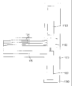
Figure 2 illustrates an antenna array 100 constructed according to the
teachings of the present invention. The antenna array 100 includes a center
element
102 surrounded by six passive elements 104A through 104F, each of which can be
operated in a reflective or a directive mode as will be discussed further
herein below.
The antenna array 100 is not restricted to six passive elements. Other
embodiments
include fewer (e.g., two or four) or more (e.g., eight) passive elements. In
yet another
embodiment where the antenna operates as a phase array, to be discussed
further
below, the center element is absent.
The center element 102 comprises a conductive radiator 106 disposed on a
dielectric substrate 108. Each passive element 104A through 104F comprises an
upper conductive segment 1 l0A through 1 l OF and a lower conductive segment
112A
through 112F disposed on a dielectric substrate 113A through 113F,
respectively.
The lower conductive segments 112A through F are grounded. Generally, the
upper
(110A-1 lOF) and the lower (112A-112F) conductive segments are of equal
length.
When the upper conductive segment of one of the passive elements (for example,
the
upper conductive segment 1 l0A) is connected to the respective lower
conductive
segment (the lower conductive segment 112A) the passive element 104A operates
in a
reflective mode such that all received radio frequency (RF) energy is
reflected back
from the passive element 104A toward the source. When the upper conductive
segment 110A, for example, is open (i.e., not connected to the lower
conductive
segment 112A) the passive element 104A operates in a directive mode in which
the
passive element 104A essentially is invisible to the propagating RF energy
which
passes therethrough.
CA 02503031 2005-04-19
WO 2004/040689 PCT/US2003/033776
-1 1-
In one embodiment, the center element 102 and the passive elements 104A
and 104D are fabricated from a single dielectric substrate, such as a printed
circuit
board, with the respective antenna elements disposed thereon. The passive
elements,
104B and 104C are disposed on a defornlable or flexural substrate and attached
or
mounted to one surface of the center element 102. Thus the passive elements
104B
and 104C are foldable into a compact arrangement when not in use, and
deformable
into the radial positions illustrated in Figure 2 for optimum operation. This
is
accomplished by folding (or deforming) the passive elements 104B and 104C
about
the attachment point toward the passive element 104A and 104D, respectively.
Similarly, the passive elements 104E and 104F are disposed on a deformable or
flexural substrate and attached or mounted to an opposing surface of the
center
element 102 so that the passive elements 104E and 104F are foldable into a
compact
arrangement when not in use or deployable into the configuration illustrated
in Figure
2 during operation. In another embodiment, each of the passive elements 104A
through 104F are formed on a separate flexible dielectric substrate and
deformably
jointed to the center element 102. In still another embodiment, the passive
elements
104A through 104F are formed on individual rigid dielectric substrates and
deformably joined to the center element 102 by use of a deformable material
interposed therebetween.
There are many devices and techniques available for attaching the deformable
substrates carrying the passive elements 104A through 104F to the center
element
102. An adhesive can be used to joint the surface of the center element 102 to
the
deformable substrates or the deformable material. Solderable vias can also be
disposed into each of the surfaces to be mated. The joints are mated and the
vias
soldered so that the joints remain deformable. If it is required for signals
to pass
between the center element 102 and each of the passive elements 104A through
104F,
then in another embodiment the solderable vias are connected to the
appropriate
conductive traces disposed on the center element 102 and the passive elements
104A
through 104F. In this way, the soldered mated vias establish an electrical
interconnection and a mechanical union between the passive elements 104A
through
104F and the center element 102. Also, a mechanical fastener can also be
utilized to
joint the various passive elements 104A through 104F to the center element
102.
CA 02503031 2005-04-19
WO 2004/040689 PCT/US2003/033776
-12-
In yet another embodiment the center element 102 and the passive elements
104A and 104D are fabricated on a first deformable substrate, the passive
elements
104B and 104C are fabricated on a second deformable substrate and the passive
elements 104E and 104F are fabricated on a third defonnable substrate. The
three
deformable substrates carrying the antenna elements are jointed as discussed
above.
In yet another embodiment, the center element 102 is formed of a rigid
dielectric
material, for example, printed circuit board, while the passive element 104A
is
disposed on a first defonnable substrate, the passive elements 104B and 104C
are
formed on a second deformable substrate, the passive element 104D is formed on
a
third deformable substrate and the passive element 104E and 104F are disposed
on a
fourth defonnable substrate. The four defonnable substrates are then joined to
the
center element by way of soldered vias or an adhesive as discussed above.
In still another embodiment of the present invention, each of the passive
elements 104A through 104F is disposed on a rigid dielectric substrate
material and
joined to the center element 102 by way of a deformable union. In particular,
one
edge of defonnable or flexural material is attached to each of the passive
elements
104A through 104F and the opposing edge of the material is attached to the
center
element 102. Thus in this embodiment, each antenna element is disposed on a
rigid
deformable material. Solderable vias or an adhesive are used to affix the
deformable
material to the center element 102.
A top view of the antenna array 100 is illustrated in Figure 3. In particular,
the
fonnable joints 1 OS are shown. Figure 4 is a top view of the antenna array
100 in a
folded configuration. The distance between adjacent passive elements (for
example,
between the passive elements 104A and 104B) is exaggerated in Figure 4 for
clarity.
The deformable joints allow the adjacent elements to come into contact so that
the
antenna array 100 is storable in a very compact configuration. Figure S is a
perspective view of the antenna 100 is a folded configuration. Although the
performance will be degraded, it is possible for the antenna array 100 to
operate in the
folded configuration of Figures 4 and 5.
Returning to Figure 2, there is shown a microelectronics module 116A through
116F interposed between the upper conductive segments 1 l0A through 1 l OF and
the
lower conductive segments 112A through 112F of each passive element 104A
CA 02503031 2005-04-19
WO 2004/040689 PCT/US2003/033776
-13-
through 104F. There is further shown a microelectronics module 122 disposed on
the
dielectric substrate 108, comprising, for example, transceiver circuitry.
Conductive
traces 124 conduct signals between the microelectronics module 112 and of the
microelectronics modules 116A through 116F. The signals carned on the
conductive
traces 124 control components within the microelectronics modules 116A through
116F for operating the passive elements 104A through 104F in either the
reflective or
the directive state. Further connected to the microelectronics module 122 is
an
interface 125 for providing electrical connectivity between the antenna array
100 and
the external communications device. The interface 125 can be constructed from
either rigid or flexible material for interfacing (via a ribbon cable, for
example) to a
connector mounted on an enclosure enclosing the antenna array 100. In use, a
conductor is inserted into the connector for connecting the antenna array 100
to the
external device. It will be appreciated by those skilled in the art that
various
placements and conductor routing paths are available for the microelectronics
modules and the conductive traces, as required for a specific antenna design
and
configuration.
Figure 6 is an enlarged view of one of the passive elements 104D, for example
including the microelectronics module 116D and the conductive traces 124. The
other passive elements are similarly constructed. The dielectric substrate
113D
comprises a deformable (flexural) material or a rigid material having a first
portion on
which the upper conductive segment 110D and the lower conductive segment 112D
are formed, and a second arm portion perpendicular to the first portion. In
the
embodiment where the passive element 104D is constructed of rigid material,
the
second arm portion includes a deformable material (not shown in Figure 6)
affixed to
the end of the second arm portion. In one embodiment, the first portion
carrying the
upper and lower conductive segments and the second arm portion are formed by
shaping or cutting a single sheet of the dielectric substrate material. The
rigid
embodiment can be formed from printed circuit board material including FR4
material, and the deformable embodiment can be formed from Kapton, polyimide,
mylar, or any other deformable material. The selection of a suitable material
is based
on the desired mechanical and electrical properties of the antenna elements,
including
loss, permittivity and permeability. Three exemplary conductive traces 124
traversing
CA 02503031 2005-04-19
WO 2004/040689 PCT/US2003/033776
-14-
the arm portion of the dielectric substrate 113D and connected to contacts
(not shown)
of the microelectronics module 116D are shown. Depending upon the
characteristics
of the switch employed within the microelectronics module 116D (to be
discussed in
conjunction with Figure 7) fewer than three conductive trace 125 may be
required for
controlling that switch. Finally, as shown, a conductive trace 125 connects
the lower
conductive segment 112D to a grounded terminal, for example on the interface
125
shown in Figure 2. The microelectronics module 116A is not confined to a
switching
function, but can include other functions related to operation of the antenna
array 100
and its constituent elements. As is known to those skilled in the art,
conductive
material for forming the upper conductive segment 110D, the lower conductive
segment 112D and the conductive traces 124 can be applied to the dielectric
substrate
by printing conductive epoxies or conductive inks thereon. Also, the
conductive
elements are formable by etching away the unwanted portions from a copper clad
dielectric substrate.
Figure 7 illustrates an exemplary microelectronics module 116D, including a
mechanical SPDT switch 140. Those skilled in the art recognize that the
mechanical
switch 140 is a simplistic representation of a switching device typically
implemented
with a junction diode, a MOSFET, a bipolar junction transistor, or a
mechanical
switch, including one fabricated using MEMS technology (microelectromechanical
system). Under control of a signal carried on one of the conductive traces
124, the
switch 140 is switched between contact with a conductor 142 and a conductor
144.
When switched to the conductor 142, the upper conductive segment 100D is
connected to an impedance element 146. The impedance element 146 compensates
for reactances (i.e., capacitive or inductive) within the switch 140 so that
the upper
conductive segment 1 lOD sees an open circuit when the switch 140 closes into
the
conductor 142. Alternatively, when the switch 140 connects to the conductor
144, the
upper conductive segment 110D sees a grounded lower conductive segment 112D
via
an impedance element 148. The impedance element 148 cancels any reactances
(i.e.,
capacitive or inductive) created in the switch 140 so that the upper
conductive
segment 1 l OD sees a short to ground. In one embodiment, there are shown
three
conductive traces 124, for carrying a positive and negative bias voltage for
biasing the
electronic component implementing the SPDT switch 140, and further a control
CA 02503031 2005-04-19
WO 2004/040689 PCT/US2003/033776
-15-
voltage signal for selecting the switch position. Depending upon the specific
electronic or mechanical component implementing the switch 140, only a
positive or a
negative bias voltage may be required or the component may be switched without
a
bias voltage ad determined solely by a control voltage. Thus, other
embodiments of
the present invention may require numbers of conductive traces 124 connected
to the
microelectronics module 116D.
Figure 8 illustrates another embodiment 300 of an antenna array according to
the teachings of the present invention, wherein the passive elements and the
center
element in the Figure 8 embodiment are similar to those illustrated in Figure
2. Each
of the passive elements 104A, 104B, 104D and 104E is disposed on a rigid
substrate
(e.g., FR4 material) and joined to the center element 102 via a deformable
material,
such as mylar, as indicated by a reference character 302. The passive elements
104F
and 104C are disposed on the same substrate as the center element 102.
In yet another embodiment of the antenna array 318 illustrated in Figures 9A
and 9B, the passive elements 104A and 104B are formed on a first deformable
material, the passive elements 104D and 104E are formed on a second deformable
material, and the center element 102 and the passive elements 104C and 104F
are
formed on a third defonnable material. The three deformable materials are
joined
together using an adhesive or mating vias soldered together to create the
deformable
union 320. The antenna array 318 is illustrated in the deployed configuration
in
Figure 9B and in the stowed configuration in Figure 9A. In a derivative
embodiment,
the antenna array 318 does not include the center element 102, such that the
six
antenna elements surrounding the deformable union 320 operate as an antenna
phased
array.
In the various embodiments discussed herein, for optimum antenna
performance each of the passive elements 104A through 104F must be oriented at
a
specified angel or range of angles with respect to each other and the center
element
102 (in those embodiments where a center element is present). This can be
accomplished by mounting the antenna array on a base surface (now shown) and
placing marks or mechanical stops on the base surface to ensure that each of
the
passive elements 104A through 104F is deployed to the correct position.
Alternatively, if the antenna is mounted within a case or enclosure, various
CA 02503031 2005-04-19
WO 2004/040689 PCT/US2003/033776
-I 6-
mechanical structures or stops can be incorporated into the enclosure so that
in the
deployed orientation, each of the passive elements 104A through 104F is
situated at
the optimum position.
Figures l0A and lOB illustrate another embodiment of the present invention,
that is an antenna array 350 including four elements 351, 354, 356 and 358
each
formed on a rigid dielectric substrate. As can be seen, the antenna elements
352 and
254 are formed on individual deformable substrates and jointed by deformable
material 360. Similarly, the antenna elements 356 and 358 are formed on
individual
sheets and jointed by material 362. The deformable materials 360 and 362 are
jointed
at a junction 364. As discussed above, vias can be utilized to create the
junction 364
or the materials can be joined by an adhesive process. Figure lOB illustrates
the
antenna array 350 in a stowed configuration.
Figure 11 illustrates the deployed state of an antenna array 370 comprising
four elements 372, 374, 376 and 378 disposed on flexible or deformable
material and
joined at a junction 380. Conventionally, since the antenna arrays 350
(Figures l0A
and lOB) and 370 (Figure 11) lack a center element, they operate as phased
array
antennas for scanning the antenna beam as desired.
Figures 12A and 12B illustrate a five element antenna array 390 including
elements 392, 394, 396, 398 and 400. In the Figure 12A and 12B embodiment the
elements 392 through 400 are disposed on a rigid dielectric substrate and
joined at a
deformable union. As can be seen, the antenna elements 392 and 400 are formed
on
individual dielectric substrates and joined to deformable material 402. The
elements
394 and 396 are also formed separately and joined by deformable material 400.
Finally, the element 398 includes a joining surface 406. The deformable
materials
402 and 404 and the joining surface 406 are mated and attached either
adhesively or
through mating vias as discussed above. The antenna array 390 is shown in the
folded
or stowed configuration in Figure 12B.
Figure 13 illustrates an antenna array 410 having five elements 412, 414, 416,
418 and 420 disposed on flexible or deformable material. In particular, the
antenna
elements 412 and 420 are disposed on a single sheet of deformable material and
the
antenna elements 414 and 416 are likewise disposed on a sheet of single
material.
The antenna element 418 is disposed on a single sheet of deformable material.
As can
CA 02503031 2005-04-19
WO 2004/040689 PCT/US2003/033776
-17-
be seen, the elements 412 through 420 are then joined at a mating junction 422
created by adhesively connecting or soldering vias as discussed above. In
another
embodiment (not shown) a center element can be disposed on the same deformable
material as the antenna element 418.
An antenna array 430 is illustrated in the deployed configuration in Figure
14A and the folded or stowed configuration in Figure 14B. The antenna array
430
includes antenna elements 432, 434, 436, 438, 440 and 442. The antenna
elements
are joined in a center hub 443 using the soldered vias or adhesive techniques
described above. The antenna array 430 includes radii 444 on each side of the
element 432 and the element 438. As shown in Figure 14B, the use of the radii
444
provides a more compact stowed configuration as each of the remaining elements
434, 436, 440 and 442 fit within the radii 444.
A five element antenna array 450, including a center element is shown in
Figures 15A and 15B. Radial elements 452, 454, 456 and 458 are spaced apart
from a
center element 460. The elements 452, 454, 456 and 458 in one embodiment are
disposed on a flexible or deformable material 462 (not shown in Figure 15A),
while in
another embodiment, the elements 452, 454, 456 and 458 are disposed on a rigid
dielectric substrate and attached to deformable material 462. The various
sheets of
deformable material 462 are joined at the center element 460 using the same
techniques in the folded configuration in Figure 1 SB.
Figures 16A and 16B illustrate another embodiment of the antenna array 450,
including an additional antenna element 451. Thus the antenna array 450 as
illustrated in Figures 16A and 16B is a five element array. Due to the odd
number of
elements, one of the elements, specifically, the element 451 is disposed
singly on a
rigid dielectric material, which is in turn mated with the deformable material
462, and
joined to the other two pairs of elements and to the center element 460 as
shown in
Figure 16A. The techniques for attaching the elements 451, 452, 454, 456 and
458 at
the center element 450 are discussed above. Figure 16B illustrates the antenna
array
450 wherein the five elements are shown in the folded or stowed configuration.
Figures 17A and 17B illustrate an antenna array having seven elements
including radial elements 482, 484, 486, 488, 490 and 492 and a center element
494.
In one embodiment as shown, the radial elements 482 and 494 are disposed on a
rigid
CA 02503031 2005-04-19
WO 2004/040689 PCT/US2003/033776
-18-
dielectric material and joined by way of a sheet of defornlable material 496.
The
radial elements 488 and 490 are likewise constructed and joined by way of a
sheet of
deformable material 497. In both cases, the radial elements can be disposed on
the
rigid dielectric material by printing or etching. The radial elements 486 and
492 and
S the center element 494 are disposed on a rigid dielectric substrate 498. The
deformable sheets 496 and 497 are attached to the center element 494 by way of
vias,
an adhesive or a mechanical fastener as discussed above. The antenna array 480
is
shown in the folded or stowed configuration in Figure 17B. In another
embodiment
(not shown) the radial elements 482, 484, 486, 488, 490 and 492 are disposed
on
flexible or deformable material and joined as shown.
The teachings of the present invention have been described in conjunction
with various antenna arrays having an active center element and a plurality of
radial
elements spaced apart therefrom, or having only a plurality of spaced apart
radial
elements operation as conventional phased arrays or digital beam formers. In a
first
such embodiment, the antenna array comprises a plurality of active or passive
elements, including a single active element at the center and a plurality of
radially
spaced apart active or passive elements deformably joined to the center active
element. In another embodiment, each of the radial elements is joined to one
or more
other radial elements at the central intersecting point. Control signals and
radio
frequency signals are input to or received from the various antenna
embodiments
through an interface (similar to the interface 125 of Figure 2) affixed to
the.
intersecting point of the plurality of antenna elements. Various devices and
techniques are known and available for attaching the antenna elements to the
center
element or to a center point if the center element is absent. Included among
these
devices and techniques are solderable vias, adhesives, and mechanical
fasteners as
discussed above.
While the invention has been described with references to a preferred
embodiment, it will be understood by those skilled in the art that various
changes may
be made and equivalent elements may be substituted for the elements of the
invention
without departing from the scope thereof. The scope of the present invention
further
includes any combination of the elements from the various embodiments set
forth
herein. In addition, modifications may be made to adapt a particular situation
to the
CA 02503031 2005-04-19
WO 2004/040689 PCT/US2003/033776
-19-
teachings of the present invention without departing from the essential scope
thereof.
Therefore, it is intended that the invention not be limited to the particular
embodiment
disclosed as the best mode contemplated for carrying out this intention, but
that the
invention will include all other constructions falling within the scope of the
appended
claims.