Note : Les descriptions sont présentées dans la langue officielle dans laquelle elles ont été soumises.
CA 02504281 2005-04-15
2
POWER MOS VOLTAGE REGULATOR FOR BATTERIES
BACKGROUND OF THE INVENTION
This invention refers to an automatic system for charging
batteries, and in particular is directed to a voltage regula-
tor of a battery charging system normally used for powering
motor vehicles, such a motorcycles and the like.
STATE OF THE ART
A system for charging the battery of a vehicle, normally
comprises a voltage magneto generator operatively connected
to the engine of the vehicle, which can be selectively con-
nected to an electrical battery of the vehicle by means of a
controlled diode bridge, and to the earth by means of elec-
tronic switches driven by a control unit preset to detect the
charging state of the battery. A general diagram of a per se
known system for charging batteries is shown in figure 1 of
the accompanying drawings.
An automatic battery charging systems for motor vehicles,
usually comprises a voltage magneto generator, and a voltage
regulator of three-phase and parallel type, in that the use
of standard voltage regulators of series type gives rise to
excessively high output voltages at high running of the en-
gine.
Therefore, this invention is directed to a battery charg-
ing system for motor vehicles, which make use of a voltage
regulator of parallel type, with particular reference to a
three-phase regulator currently in use when the power re-
CA 02504281 2005-04-15
3
quired by the motor vehicle exceed 200 W.
As shown in figure 1, a well-known system for charging
the battery of a motor vehicle, usually comprises a voltage
magneto generator 10, having phase windings A, B and C con-
nected to a positive terminal of a battery BA by means of a
controlled diode bridge 11, substantially comprising the di-
rectly biased diodes D1, D2, D3 having the cathode connected
to the positive terminal of the battery BA, and branched-off
or reversely biased diodes D4, D5 and D6 whose anode is con-
nected to earth.
The phase windings A, B and C of the magneto generator
10, are in turn selectively connectable to the earth by means
of respective electronic switches, consisting for example of
the SCR Ql, Q2 and Q3 whose control electrode is connected to
a control unit 12 to be driven in relation to a voltage value
or a charge state of the battery BA.
This solution, although being simple, nevertheless in-
volves excessive power dissipation when the currents flowing
in the phase windings of the generator 10 become high. For
example, a voltage regulator having an output current of 30A,
dissipates approximately 60 W in the power components, since
the voltage drop in each SCR diode is approximately 1 V. This
fact also implies the need to use somewhat cumbersome finned
power dissipators.
In order to improve the situation, it has also been sug-
gested to use a regulator of parallel-type comprising Schot-
CA 02504281 2005-04-15
4
tky diodes and power MOS transistors.
By means of this second solution it is possible to reduce
the power dissipation in that a power MOS transistor, for
voltages lower than 60 V, in a TO 220 container has a resis-
tance of approximately 5 ohm, while a Schottky diode has a
voltage drop of only 0.6 V. The dissipated power can be esti-
mated as being between 20 and 30 W depending upon the ON or
OFF conditions of the electric loads connected to the bat-
tery.
These voltage regulators however have a number of draw-
backs that this invention aims to remedy.
One of the functional differences existing between an SCR
controlled diode and a power MOS transistor, is that the lat-
ter can be switched both in ON and in OFF state, while the
SCR controlled diode does not switch off until the current
has dropped to zero; this fact implies that in a power MOS
regulator the latter can be switched ON and OFF regardless of
the currents flowing in the components, which on the contrary
does not occur with SCR regulators in which the ON state can
be actuated at any time in relation to the charge degree of
the battery, while the OFF state occurs only when the current
reaches zero valve.
During the time in which the power MOS transistors are
OFF, the current flows exclusively between the phase windings
of the generator and the power MOS, not affecting the bat-
tery, and consequently preventing the charging of the same
CA 02504281 2005-04-15
battery. When the control unit which controls the voltage of
the battery detects that said voltage is dropped below a pre-
established rated value, then the power MOS must be switched
OFF; if this is done regardless of circulation of the cur-
rents in the phase windings of the generator, it can give
rise to current peaks with very steep fronts through the
charging diodes, the cables and the battery, with consequent
voltage peaks due to the inductances of the generator and the
same cables, negatively effecting the electronic equipments
of the vehicle.
The same applies as far as the ON switching of the power
MOS is concerned.
OBJECT OF THE INVENTION
The main object of this invention is to remedy these
problems in order to reduce the power dissipation of the
voltage regulator, and prevent the formation of high current
peaks and the consequent circuit noises.
BRIEF DESCRIPTION OF THE INVENTION
According to the invention, a voltage regulator has been
provided in an automatic voltage charging system for a bat-
tery including an AC magneto generator having at least one
phase winding selectively connectable to the battery and to
earth, said voltage regulator comprising:
a rectifier bridge having a Schottky diode connected be-
tween the phase winding of the magneto generator and the bat-
tery, and a power MOS transistor branched-off between the
CA 02504281 2005-04-15
6
phase winding and an earth terminal; and
an electronic control unit connected to a control elec-
trode of the power MOS transistor to drive the latter between
ON and OFF states, said control unit being conformed and pre-
set to detect the phase voltage of the magneto generator, re-
spectively to detect the voltage of the battery, and to trig-
ger the power MOS transistor between the ON and OFF states
when the detected phase voltage of the magneto generator is
passing through zero.
In particular, according to the invention, during each
charging step of the battery, the power MOS transistor is
maintained in a conductive or ON state when the voltage be-
tween the Drain and the Source of the power MOS is negative,
and in a OFF state when the voltage between the Drain and the
Source of the power MOS is positive, whereas if the voltage
of the battery is higher than its rated charging value, the
power MOS transistor is maintained constantly in its ON state
to short-circuiting the relevant phase of the magneto genera-
tor towards earth, while any change between the ON and OFF
states of the power MOS transistor always occurs when the
phase voltage of the same magneto generator, with respect to
earth, or the voltage between the Drain and Source electrodes
of the power MOS transistor passes through zero.
BRIEF DESCRIPTION OF THE DRAWINGS
These and further features of a voltage regulator and a
system for charging batteries according to this invention,
CA 02504281 2005-04-15
7
will be more clearly evident from the following description,
with reference to the accompanying drawings, in which:
Fig. 1 shows the diagram of a per se known battery charg-
ing system;
Fig. 2 shows the diagram of an electronic voltage regula-
tor and a battery charging system according to the invention;
Figs. 3A to 3E show some voltage graphs of the voltage
regulator of figure 2.
DETAILED DESCRIPTION OF THE INVENTION
Fig. 1 shows the general diagram of a system for charging
a battery of a known type, as previously described, while
fig. 2 shows a battery charging system comprising a voltage
regulator according to the invention, for a three-phase AC
magneto generator; however, the invention can be applied to
any type of single-phase and multi-phase voltage generator,
depending upon the circumstances.
For ease of description, reference will be made to a sin-
gle phase of a three-phase voltage generator 10, for example
to the phase winding A, in that the proposed electronic solu-
tion should be understood as repeated for the remaining phase
windings B and C, in the three-phase system of fig. 2.
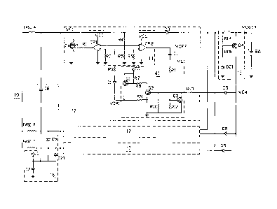
As shown in fig. 2, each of the phase windings A, B and C
of the AC voltage magneto generator 10, is connected to the
positive terminal (+) of the battery BA, by means of a recti-
fier bridge comprising, a directly biased diode D3, such as a
"Schottky" diode, having a low conductive resistance and a
CA 02504281 2013-07-11
8
low voltage drop. The anode of the Schottky diode D3, as
shown, is connected to the phase winding A of the voltage
generator 10, while its cathode is connected to the positive
terminal (+) of the battery BA.
The rectifier bridge also comprises, for each phase of
the voltage generator 10, a power MOS transistor Ti, which is
branched-off between the phase winding A and the earth; more
particularly, the Drain electrode D of Ti, is connected to
the phase winding A, as per the anode of diode D3, while its
Source electrode S is connected to the earth of the circuit.
In the same fig. 2 it can also be seen that the control
or Gate electrode G of the transistor Ti is connected to the
outlet side of an electronic control unit 12, the inlet side
of which in turn is connected, by means of diode D5, to a
first voltage detecting circuit 13; the circuit 13 detects
the high and low states of the charging voltage Vbatt of the
battery BA, in relation to which the control unit 12 drives
the power MOS transistor Ti between its ON and OFF states.
The control unit 12 comprises a memory M1 for memorising
a high and a low state of the voltage of the battery BA, to
be compared to a rated voltage value; the inlet of the memory
M1 is connected to the voltage detecting circuit 13 by means
of a resistor R13 and the diode D5.
A first outlet VOM1 of the memory M1 is in turn connected
to a second voltage detecting circuit 14 for detecting the
alternating voltage VF1 of the phase winding A of the voltage
CA 02504281 2005-04-15
9
generator 10.
More in particular, according to a possible embodiment,
the memory M1 comprises two electronic switches Q1 and Q2,
consisting of a PNP and respectively a NPN transistor; the
collector-emitter circuit of Q1 is directly connected to the
voltage outlet VCC of a feeding circuit 16, while the control
base of Ql is connected to a voltage divider provided by the
resistors R7 and R8 in the emitter-collector circuit of Q2.
The control base of Q2 is in turn connected to a voltage di-
vider provided by the resistors R9, R10, and is connected to
a reset circuit for resetting the memory Ml, comprising an
electronic switch Q3 such as a NPN transistor, whose base is
polarised by a resistor R12.
The emitter-collector circuit of Ql, by means of the out-
let VOM1 of the memory Ml, is also connected to the AC volt-
age detecting circuit 14 for controlling the voltage VF1 of
the phase winding A.
The AC voltage detecting circuit 14 comprises a first
voltage comparator CP1 whose outlet is connected to the Gate
or control electrode of the power MOS Ti by means of the re-
sistor Rl.
The circuit 14 also comprises a second voltage comparator
CP2 whose outlet is connected, by means of the capacitor Cl,
to a voltage divider of the memory Ml, provided by the resis-
tors R11 and R12.
The non-inverting inlet (+) of the first voltage compara-
CA 02504281 2005-04-15
tor CP1 is connected, by means of the resistor R3 and the di-
ode D1 to the outlet VOM1 of the memory circuit Ml, and to
earth by means of the resistor R2.
Lastly, in the same figure 2 it can be seen that the in-
verting inlet (-) of both voltage comparators CP1 and CP2,
are connected, by means of a voltage divider R4, R5 to the
phase winding A.
Reference 16 in figure 2 has been used to indicate a DC
feeding circuit for the system, connected between the phase
10 windings A, B, C of the voltage generator 10 and earth, by
means of the diodes D8, D9 and D10 and the capacitor C2, to
supply a feeding voltage VCC to the components, substantially
corresponding to the battery voltage Vbatt.
Lastly, the voltage detecting circuit 13, for detecting
the charge degree of the battery BA, comprises a PNP transis-
tor Q4 whose emitter-collector circuit is connected to the
inlet side of the memory M1 by means of the diode D5 and the
resistor R13, while the base of Q4 is connected to a voltage
divider R14, R15 comprising a Zener diode DZ1.
The voltage regulator operates as follows.
Let us consider the step in which the battery BA must be
charged because its voltage value is lower than a desired
threshold or rated voltage: typically 14.5 Volt.
As can be seen from fig. 2, the comparator CP1 detects
the passage through zero of the voltage of phase winding A;
in particular the outlet of the comparator CP1 connected to
CA 02504281 2005-04-15
11
Gate G of Ti, switches low bringing the power MOS Ti into an
OFF state when the voltage of phase A is positive with re-
spect to earth; therefore the Schottky diode D3 will be bi-
ased directly and the current coming from phase winding A of
the generator can charge the battery BA.
When the voltage of phase A of the generator 10 is nega-
tive with respect to earth, the outlet of the comparator CP1
connected to Gate G of Ti, switches high bringing the power
MOS Ti into an ON state; therefore the current can flow from
earth, through the power MOS Ti, towards phase winding A of
the generator.
If during this time the Gate G of Ti remains low, the
current from earth can go to phase winding A of the generator
through the diode inside the power MOS, which has its anode
connected to the Source and its cathode to the Drain; how-
ever, in this way the voltage drop and therefore the power
dissipation are greater.
A power MOS diode with a resistance of 5 milliOhms, with
a breakdown voltage of 60 Volts and a current of 30 Amp, has
a voltage drop of 0.15 Volts, while in the event the diode is
in a conductive state, the voltage drop of the diode is at
least 0.7 Volts, thereby proving the importance of bringing
the power MOS Ti into an ON state when the phase voltage is
negative.
The system is also provided with a second voltage com-
parator CP2 having its inverting inlet (-) in common with the
CA 02504281 2005-04-15
=
12
inverting inlet (-) of CP1, both being connected, by means of
the voltage divider R4, R5, to phase winding A of the genera-
tor 10; the non-inverting inlet (+) of CP2 is connected to
earth by means of the resistor R6. The voltage comparator CP2
reads the voltage drop at the terminals of the power MOS Ti
and provides a square wave output signal VF1 (figure 3A)
which is reversed with respect to the voltage signal of the
relevant phase winding A of the generator 10.
If the battery voltage Vbatt is lower than the voltage of
the Zener diode DZ1, then no current flows through the volt-
age divider R14, R15 and the PNP transistor Q4 cannot enter
into an ON state. As a result, neither the transistors Ql, Q2
can enter into their ON state; consequently the diode D1 is
interdicted or in an OFF state and the non-inverting inlet
(+) of CP1 is referred to earth by means of the resistor R2.
Since the inverting inlet of CP1 is in common with the in-
verting inlet (-) of CP2, during this step the comparator CP1
behaves like CP2 thus being able to drive Ti in an OFF state
when phase voltage of winding A of the generator is positive
with respect to earth, and drive Ti in an ON state when phase
voltage of winding A of the generator is negative with re-
spect to earth.
During the positive fronts of the output voltage VCP2
(fig. 3B) of the comparator CP2, by means of the capacitor Cl
and the voltage divider R11, R12, Q3 enters into an ON state
for a very short time, typically 10 microseconds determined
CA 02504281 2005-04-15
13
by the capacity value of the capacitor Cl, and by the resis-
tor R11, but since the transistor Q2 is already in an OFF
state, as Ql, the state of the transistor Q3 has no effect on
the state of the memory Ml; the capacitor Cl will later be
discharged during the negative fronts at the outlet of CP2
(VC1 fig. 3C).
The assembly comprising the transistor Ql and the tran-
sistor Q2 with the resistors R7, R8; R9, R10 connected as
shown in fig. 2, constitutes a memory circuit for the high
and low states of the battery voltage Vbatt, with respect to
its rated value.
The outlet of the aforesaid memory has a voltage VOM1 ap-
plied to the anode of D1, which is null if Ql and Q2 are in
an OFF state, and at a voltage value equivalent to VCC if Ql,
Q2 are in an ON state, as shown in figure 3E.
Ql is brought into the ON state when Q2 is in a conduc-
tive or ON state, the latter in turn being activated by the
positive biasing of its base generated by a current entering
the base of Q2 through D5 and R13, when Q4 is ON.
Since there is a positive reaction of the outlet on the
inlet through R9, if Ql and Q2 are ON, they will remain so
regardless of the state of Q4; Ql, Q2 will go back to the OFF
state only when Q3 is brought ON, thereby giving rise to the
resetting of the memory Ml.
In practice, the outlet VOM1 of the memory M1 can switch
from the logic state 1 to the logic state 0 only in corre-
CA 02504281 2005-04-15
14
spondence with the leading front of the output of the com-
parator CP2 (fig. 3B) which, by means of Cl and Rll bring Q3
into the ON state, and can switch from the logic state 0 to 1
only with a positive signal on the base of Q2 generated by Q4
through D5, R13.
If the battery voltage exceeds the voltage of the Zener
DZ1, which indicates that the battery BA has reached the full
load voltage, the current begins to flow through the voltage
divider R14, R15 biasing the base of the transistor Q4 until
it begins to conduct, bringing the voltage VE4 (fig. 3D) on
the anode of the diode D5, up to the battery voltage Vbatt;
being biased directly, the diode D5 conducts and sets the
memory M1 of winding A, and at the same those of the other
phases winding B and C, at the logic state 1.
The output voltage VOM1 of the memory Ml, relating to the
logic state 1, corresponds to VCC which is equal to the bat-
tery voltage Vbatt, which is also equal to the phase voltage
VF1, less the voltage drop of the Schottky diode D3 (typi-
cally 0.5 Volt), when the latter is ON or in a conductive
state.
If, as shown in fig. 3, the voltage VE4 switches from 0
to Vbatt in correspondence with the high phase voltage VF1,
that is to say while phase winding A is loading the battery
BA, the outlet VOM1 of the memory M1 switches from the logic
state 1 corresponding to the voltage VCC, which is divided by
the resistive voltage divider R3, R2 and applied to the non-
CA 02504281 2013-07-11
inverting inlet of CP1, while the voltage VF1 divided by the
resistive potential divider R4, R5 is present at the invert-
ing input.
If the resistive values are chosen in such a way that
R3/R2>R4/R5, for example R3=3R2 and R4=R5, then during the
time in which the phase voltage VF1 is high, that is to say
it is at a voltage of approximately 0.5 Volts higher than
that of the battery, the inverting inlet of CP1 still exceeds
the non-inverting inlet, whose outlet remains low, preventing
10 Ti from entering into conduction, while the Schottky diode D3
is ON. In this way it is possible to avoid the problems of
voltage peaks due to the rapid change of current in the di-
odes and in the connecting cables.
This is due to the fact that the current flowing from the
voltage regulator 12, towards the battery BA, has a sinusoi-
dal pattern imposed by the alternating voltage of the genera-
tor 10, and not by the switchover of the electronic switches.
When the voltage VF1 changes from positive to negative,
the outlet of CP1 is still high and Ti is still ON or in a
conductive state, while the outlet of the comparator CF2
switches from low to high and, by means of the capacitor Cl
and the resistor R11, brings the transistor Q3 into the ON
state for a few microseconds sufficient to bring the outlet
VOM1 of the memory Ni to the logic state 0.
The voltage VF1 is negative with respect to earth by a
few tenths of a Volt determined by the voltage drop generated
CA 02504281 2005-04-15
16
by the current which flows through the power MOS Ti, from
earth towards phase winding A.
If the voltage VE4 remains high, which indicates that the
battery BA is loaded, then the outlet of the memory M1 is
once again brought into the logic state 1 corresponding to a
voltage VOM1=VCC subsequently applied, by means of the diode
D1 and the voltage divider R3, R2, to the non-inverting inlet
(+) of the comparator CP1, which inlet will be to a voltage
value equivalent to a fraction of VCC.
When the voltage VF1 changes from negative to positive
then, since Ti is in the ON state, the voltage applied to the
inverting inlet (-) of CP1 is lower than the voltage applied
to the non-inverting inlet (+) and therefore the outlet of
CP1 remains high with Ti in the ON state.
When the voltage VE4 drops to zero, indicating that the
battery is exhausted, and assuming as in fig. 3D that this
occurs at the time ti at which VF1 is positive, the state of
the memory M1 does not change, that is to say, VOM1 remains
high until the voltage VF1 passes through zero value, from
positive to negative in correspondence with the leading front
of VCP2.
In this way it is possible to avoid having rapid current
changes in the connecting cables between the voltage regula-
tor and the battery and in the Schottky diodes, due to the
rapid switchovers of the power MOS Ti, for the reasons men-
tioned previously.
CA 02504281 2005-04-15
17
In practice, the power MOS Ti changes state, that is to
say, it passes from ON to OFF state, and vice versa, only in
correspondence with the passage through zero of the voltage
VF1, which also corresponds to current null in that the sys-
tem described detects the voltage drop on Ti, with respect to
earth.
Obviously, what has been described for the phase winding
A applies to all the other phase winding of a multiphase gen-
erator-voltage regulator system, a single phase generator
connected to the battery BA by a single phase diode bridge
having the same features previously described.
From what has been described and shown in the accompany-
ing drawings, it will be clear that a power MOS voltage regu-
lator for charging the batteries of motor vehicles, or for
other purpose, and a system for automatically charging bat-
teries comprising a similar voltage regulator, has been pro-
vided, whereby it is possible to achieve the desired results.
It is understood however that other modifications or
changes may be made to the various components of the voltage
regulator, and the entire battery charging system, without
deviating from the scope of the appended claims.