Note : Les descriptions sont présentées dans la langue officielle dans laquelle elles ont été soumises.
CA 02508867 2005-06-O1
1
LIQUID EJECTING HEAD AND
LIQUID EJECTING APPARATUS USABLE THEREWITH
FIELD OF THE INVENTION AND RELATED ART:
The present invention relates to a liquid
ejecting head for ejecting liquid such as ink and a
liquid ejecting apparatus using the same. The liquid
ejecting apparatus is applicable to an ordinary
1o printer which effects recording by ejecting ink, a
copying machine, a facsimile having a communication
system, a multi-function recording device having such
functions in combination, or the like, and in addition
to an apparatus for drawing a figure or a pattern by
ejecting liquid other than ink.
It has been proposed that ink jet recording
head which is a typical one of liquid ejecting heads
is provided on an ink jet recording substrate with a
ROM (Read Only Memory) to store data such as
2o individual information for the particular head such as
its ID (Identity) cord, a driving particularly
property of its ink ejecting mechanism. For example,
Japanese Laid-open Patent Application Hei 3 - 126560
discloses an ink jet recording head having an EEPROM
(Electrically Erasable Programmable ROM).
It is known that heat generating resistors for
generating energy for ink ejection is constituted in a
CA 02508867 2005-06-O1
2
plurality of lamination film layers on a base portion
of an ink jet recording substrate of the ink jet
recording head, and a resistance indicative of
information peculiar to the head (or individual
information) is formed. This is useful when the amount
of the information to be store is relatively small.
The peculiar information of the peculiar is acquired
by the ink jet recording apparatus on which the ink
jet recording head is mounted reading the value of the
to resistance of the resistor formed on the base
substrate, on the basis of which the ink jet recording
apparatus side can effect optimum drive controls for
the liquid ejection from the ink jet recording head.
Japanese Laid-open Patent Application Hei
6 - 91877 discloses that when the lamination film
layers constituting the ink ejection portion are
formed on the base substrate for manufacturing the ink
jet recording, a fuse (ROM) is simultaneausly formed.
By selectively melting the fuse by controlling a logic
2o circuit formed simultaneously, binary data can be
written and stored on the basis of the state of the
fuse.
With the ink jet head using such an ink jet
recording substrate, the peculiar information of the
head is stored, and still, the structure is simplified,
and the production property and cost saving is good.
In the case of such an ink jet recording head
CA 02508867 2005-06-O1
3
as is capable of recording the information, a measure
should be taken against static electricity.
Particularly, in the case of an ink jet recording head
detachably mountable to a main assembly of the ink jet
recording apparatus, the ink jet recording head is
necessarily touched by the user's hand or fingers upon
the mounting thereof to the main assembly of the
apparatus. For example, when the head and the ink
container are integral, an ink jet recording head is
to mounted each time the ink in the ink container is used
. up, and the head is touched by the user's hand or
fingers each time the mounting. When an ink jet
recording apparatus is selectively usable as a normal
image quality recording machine or as a photographic
(high image quality) recording machine by replacing
the recording head with that of another kind, the ink
jet recording head is touched by the user each time of
replacement. In such operations, it is desirable to
protect the ink jet recording head from static
2o electricity attack. For such a purpose, Japanese
Laid-open Patent Application Hei 07 - 06095 3
discloses provision of an electrical discharge circuit
around contact pads for electrical connection with the
main assembly of the ink jet recording apparatus.
However, the conventional ink jet recording
head capable of storing the information involves the
following problems:
CA 02508867 2005-06-O1
4
The ink jet recording head having the storing
element such as ROM or EEPROM disclosed in Japanese
Laid-open Patent Application Hei 3 - 126560 or
Japanese Laid-open Patent Application Hei 6 - 9187 7,
unavoidably has a complicated structure, and therefore,
various improvements for a high production property or
for reduction in size and weight are desired.
Fundamentally, a ROM chip is advantageous when the
amount of recording data is large, but it is
1o disadvantageous when the amount is small.
In addition, the problem of the static
electricity is not taken into account. When the size
of the storing element for storing the peculiar
information on the head substrate, the contact for
outputting the peculiar information of the head is
relative weaker against the static electricity attack,
and therefore, the there is a liability that storing
element is broken, or the content of the stored
information is changed when the head is touched by the
user. In view of this, measurement against the static
electricity attack is important.
In the ink jet recording head disclosed in
Japanese Laid-open Patent Application Hei 07 - 06095
33, the influence of the static electricity can be
avoided, but it is required to provide a discharge
circuit on the substrate separately. For this reason,
improvements in the space efficiency, downsizing
CA 02508867 2005-06-O1
and/or cost reduction are desired.
SUMMARY OF THE INVENTION:
5 Accordingly, it is a principal object of the
present invention to provide a liquid ejecting head
and a liquid ejecting apparatus usable therewith
wherein the influence of the static electricity is
suppressed with a simple~structure.
to It is another object of the present invention
to provide a liquid ejecting head and a liquid
ejecting apparatus wherein the discharge during
handling of the liquid ejecting head more easily
occurs to a voltage source contact pad or a grounding
contact pad than to an information output contact pad,
by which the problem of the breakdown of unintentional
overwriting or rewriting of the information in the
storing element due to the electric discharge is
minimized.
2o According to an aspect of the present invention,
there is provided a liquid ejecting head for ejection
liquid, comprising electric wiring member including a
plurality of contact pads which are electrically
contactable to a liquid ejecting apparatus a storing
element for storing individual information; a liquid
ejection member, provided with an ejection outlet for
ejecting the liquid, for ejecting the liquid using
CA 02508867 2005-06-O1
6
electric energy supplied through a part of said
plurality of contact pads, wherein said contact pads
include an information contact pad electrically
connected with said storing element, a voltage source
contact pad for supply the electric energy and a
grounding contact pad, and said voltage source contact
pad or said grounding contact pad is disposed at each
of both sides of said information output contact pad,
with no individual information contact pad which is
1o electrically contactable to the liquid ejecting
apparatus, therebetween.
These and other objects, features and
advantages of the present invention will become more
apparent upon a consideration of the following
description of the preferred embodiments of the
present invention taken in conjunction with the
accompanying drawings.
BRIEF DESCRIPTION OF THE DRAWINGS:
Figure 1 is a schematic view of a wiring
substrate of an ink jet recording head according to a
first embodiment of the present invention.
Figure 2 is a schematic view of a wiring
substrate of an ink jet recording head according to a
second embodiment of the present invention.
Figure 3 is a schematic view of a wiring
CA 02508867 2005-06-O1
7
substrate of an ink jet recording head according to a
third embodiment of the present invention.
Figure 4 is a schematic view of a wiring
substrate of an ink jet recording head according to a
fourth embodiment of the present invention.
Figure 5 is a perspective view illustrating a
first ink jet recording head using the wiring
substrate shown in Figure 2.
Figure 6 is an exploded perspective view of an
1o ink jet recording head shown in Figure 5.
Figure 7 is a partly broken perspective view of
a first recording element substrate constituting the
ink jet recording head shown in Figure 5.
Figure 8 is a perspective view illustrating the
second ink jet recording head using a wiring substrate
for the ink jet recording head of Figure 1.
Figure 9 is an exploded perspective view of an
ink jet recording head shown in Figure 8.
Figure 10 is a partly broken perspective view
of a second recording element substrate constituting
the ink jet recording head shown in Figure 8.
Figure 11 is a schematic view of a Si substrate
including a fuse for storing peculiar information of
the head and peripheral circuits therefor, according
to the present invention.
Figure 12 is a schematic top plan view of an
inside of an example of a recording device usable with
CA 02508867 2005-06-O1
8
the ink jet recording head according to the present
invention.
Figure 13 is a schematic view illustrating an
ESD experiment.
DESCRIPTION OF THE PREFERRED EMBODIMENTS:
The description will be made as to the
embodiments of the present invention in conjunction
1o with the accompanying drawings.
Figure 5 to Figure 12 illustrate an ink jet
recording head or an ink jet recording apparatus which
is a liquid ejecting head or a liquid ejecting
apparatus according to the present invention. The
respective constituent-elements will be described.
The recording head of this embodiment is of a
type integral with an ink container, and may be a
first recording head H1000 filled with black ink, as
shown in (a) and (b) of Figure 5, and may be a second
recording head H1001 filled with color inks (cyan ink,
magenta ink and yellow ink), as shown in (a) and (b)
of Figure 8. The recording head H1000 or H1001 is
securely supported on a carriage 102 of a main
assembly of the ink jet recording apparatus by
positioning means and electrical contacts, and is
detachably mountable to the carriage 102. When the ink
is used up, the recording head can be replaced.
CA 02508867 2005-06-O1
9
The description will be made as to the
structures of the recording heads H1000 and H1001 in
detail.
(Recording head)
The first recording head H1000 and the second
recording head H1001 are both of a type using an
electrothermal transducer for generating thermal
energy fox creating film boiling in the ink in
response to an electric signal, and the electrothermal
to transducer functions as a recording element and is
disposed opposed to an ink ejection outlet. In this
embodiment, the recording head integrally comprises a
recording element substrate for ejecting the ink (in
this embodiment, the liquid ejection member is
provided with ejection outlets for~ejecting the liquid,
and the liquid is ejected using the supplied electric
power), and an ink container for retaining and storing
the ink to be supplied to the recording element
substrate. However, the present invention is
2o applicable also to a recording head not having the ink
container integrally.
(1) first recording head H1000:
Figure 6 is an exploded perspective view of the
first recording head H1000. The first recording head
H1000 comprises a first recording element substrate
H1100, an electric wiring member (electric wiring
sheet) H1300, and an ink retention member H1500.
CA 02508867 2005-06-O1
Figure 7 is a partly broken perspective view of
the first recording element substrate H1100.
The first recording element substrate H1100 is
constituted by a Si substrate H1110 having a thickness
5 of 0.5 mm-2 mm, in which ink supply port H1102 in the
form of an elongated through-opening (ink flow path)
is formed. The ink supply port 1102 of the first
recording element substrate H1100 is in fluid
communication with the ink supply port H1200 of the
1o ink retention member H1500 by bonding and fixing the
first recording element substrate H1100 to the ink
retention member H1500 with high precision.
The Si substrate H1110 is provided with an
array of electrothermal transducer elements H1103 at
each lateral side of the ink supply port H1102, so
that arrays interpose the ink supply port H1102, and
there are further provided unshown electric wiring of
A1 and the like for supplying electric power to the
electrothermal transducer elements H1103.
2o The Si substrate H1110 is provided along edge
portions adjacent opposite ends of the arrays of the
electrothermal transducer elements H1103 with
electrode portions H1104 for supplying the electric
power to the electric wiring and for supplying the
electric signals for driving the electrothermal
transducer elements H1103, and bumps H1105 of Au are
formed at the tops of the electrode portions H1104.
CA 02508867 2005-06-O1
m
The Si substrate H1110 is further provided with
a fuse and a peripheral circuit therefor formed
thereon, the fuse being effective to store the
peculiar information of the head. Figure 11 show the
fuse and the peripheral circuit.
In Figure ll the fuse is indicated by a
reference H1117. In this example, four fuses H1117 of
polysilicon resistor are disposed adjacent: a short
side of the ink supply port H1102. Each of the fuses
1o H1117 is connected with a second driving element H1118
for melting the fuse and reading the information
corresponding to the melting or non-melting of the
fuse. The second driving element H1118 is disposed
adjacent to the first driving element H1116 for
driving the electrothermal transducer element H1103.
A signal for selecting the first driving
element H1116 for driving the electrothermal
transducer element H1103 is used as the signal for
selecting the second driving element H1118 for driving
2o the fuse H1117 as it is. Therefore, the circuit
portion for selecting the second driving element H1118
can be formed with the structure similar to the
circuit portion for selecting the first driving
element H1116. More particularly, the portion from the
signal line to which the signal is inputted outside
the ink jet recording substrate to the signal line
connected to the second driving element H1118 through
CA 02508867 2005-06-O1
12
a shift register, a latching circuit and a decoder,
may be common circuit structure with the circuit for
selecting the first driving element H1116. The
selection circuit H1112 for finally selecting the
second driving element H1118.on the basis of the
output from the shift register or the like, has a
structure similar to the selection circuit for the
first driving element H1116.
A VH pad H1104c for supplying a voltage from a
1o VH voltage source is connected with the electrothermal
transducer element H1103 through the VH wiring lead
H1114. A GNDH pad H1104d for connection with the GNDH
voltage source is commonly connected to the second
driving element H1118 connected with the fuse H1117
and the first driving element H1116 connection to the
electrothermal transducer element H1103 through the
GNDH wiring lead H1113. Namely, the GNDH wiring lead
H1113 is common for the first driving element H1116
and the second driving element H1118.
2o When the fuse H1117 is to be melted, the ID pad
H1104a functions as a fuse cutting voltage source
contact for applying a melting voltage, and when the
information indicated by the fuse is to be read out,
it functions as a signal output contact. More
particularly, when the fuse H1117 is to be melted, a
voltage (a driving voltage 24V for the electrothermal
transducer element, for example) is applied to the ID
CA 02508867 2005-06-O1
13
pad H1104a to instantaneously disconnect the
corresponding fuse H1117 by actuating the second
driving element H1118 selected by the selection
circuit. At this time, the electrical conduction
between the ID voltage source pad H1104b for reading
the information of the fuse out and the outer circuit
such as the voltage source for reading the fuse
information, is disconnected. .
On the other hand, when the information is to
to be read out, the ID voltage source pad H1104b is
supplied with a voltage (power source voltage 3.3V of
a logic circuit, for example), so that when the fuse
H1117 is disconnected, the potential of the ID voltage
source pad H1104b and that of the ID pad H1104a are
equal to each other, and therefore, a Hi level voltage
is outputted from the ID pad H1104a. When the fuse
H1117 is not melted; a Lo level voltage is outputted
from the ID pad H1104a since the fuse H1111 has a
resistance value which is far larger than the
2o resistance value of the fuse H1117.
In another example, the fuse H1117 is replaced
with a simple wiring on the Si substrate H1110, and
the presence or absence of such wiring may indicate
information to be stored and read out. In such a case,
the peculiar information of the head is written during
film formation for the wiring lead on the Si substrate
H1110. The reading of the information is exactly the
CA 02508867 2005-06-O1
14
same as the foregoing example, but it is not possible
to write information after the formation.
Tn a further example, a resistance element
representing information peculiar to the head is
s formed on the Si substrate H1110, and one end of the
resistance element is connected to the ID pad H1104a,
and the other end is connected to the GNDH pad H1104d.
In such a case, the main assembly of the ink jet
recording apparatus reads a resistance value between
to the ID pad H1104a and the GNDH pad H1104d to acquire
the peculiar information of the head corresponding to
the resistance value.
In any of such examples, structure of resin
material having an ink flow path is formed, for each
15 of the electrothermal transducer elements H1I03, on
such a side of the Si substrate H1110 as is provided
with the fuses, the wiring pattern or the resistance
element through a photolithography. The structure has
an ,ink flow passage wall H1106 for defining each of
2o the ink flow paths and a ceiling portion covering the
top part thereof, and in the ceiling portion, ejection
outlets H1107 are formed. The ejection outlets 1107
are provided opposed to the respective ones of the
electrothermal transducer elements H1103, thus
25 constituting a group of ejection outlets H1108.
In the first recording element H1100 thus
constituted, the ink supplied from the ink flow path
CA 02508867 2005-06-O1
H1102 is ejected through the ejection outlet 1107
opposed to the corresponding electrothermal transducer
element H1103 by the pressure of the creation of the
bubble caused by heat generation of the electrothermal
5 transducer element H1103.
The electric.wiring sheet H1300 is to
constitute the electric signal path for applying the
electric signal for ejecting the ink to the first
recording element substrate H1100, and is formed of a
to polyimide base material and a wiring lead pattern of
copper foil thereon. Also, an opening H1303 for -
setting the first recording element substrate H1100 is
formed, and adjacent the edge of the opening, an
' electrical contact for connection with the electrode
z5 portion H1104 of the first recording element substrate
H1100. Furthermore, the electric wiring sheet H1300 is
provided with an external signal input contact for
receiving the electric signal from the main assembly
apparatus, and an external signal input contact H1302
2o and the electrical contact H1304 are electrically
connected with each other by a continuous wiring Lead
pattern of copper foil.
The electrical connection between the electric
wiring sheet H1300 and the first recording element
substrate H1100 are electrically connected by an
ultrasonic heat crimping method between the bump H1105
formed at the electrode portion H1104 of the first
CA 02508867 2005-06-O1
16
recording element substrate H1100 and the electrical
contact H1304 of the electric wiring sheet H1300
corresponding to the electrode portion H1104 of the
first recording element substrate H1100.
On a flat surface around the first recording
element substrate H1100 fixed at the ink retention
member H1500 (that is, the surface faces to the
recording material when the recording head H1000 is
mounted on the carriage 102), a back side of a part of
to an electric wiring tape H1300 is fixed by adhesive
material. An unbonded portion of the electric wiring
tape H1300 is bent and is fixed by an adhesive
material on a side surface substantially perpendicular
to the bonding surface of the ink retention member
H1500 for the first recording element substrate H1100.
(2) Second recording head H1001
The second recording head H1001 functions to
eject three color inks, namely, the cyan ink, the
magenta ink and the yellow ink. As shown in Figure 9
2o which is an exploded perspective view, the second
recording head H1001 comprises a second recording
element substrate H1101, an electric wiring sheet
H1301 (electric wiring member), and an ink retention
member H1501. The structures of the second recording
head H1001 are similar to the first recording head
H1000 described in the foregoing.
Figure 20 is a partly broken perspective view
CA 02508867 2005-06-O1
17
to illustrate the structure of the second.recording
element substrate H1101: In the second recording
element substrate H1101, three ink supply ports H1102
for the cyan ink, the magenta ink and the yellow ink
are formed and axe extended in parallel with each
other, as is different from the first recording
element substrate H1100. At respective lateral sides
of each of the ink supply port H1102, electrothermal
transducer elements H1103 and ejection outlets H1107
are arranged staggered, generally along a line. On the
Si_substrate H1110a, similarly to the Si substrate
H1110 of the first recording element substrate H1100,
electric wiring, fuses or resistances and electrode
portions are formed. On the Si substrate H1110a, ink
flow passage walls H1106 and ejection outlets H1107
are formation of resin material through a
photolithography. At the electrode portion H1104 for
supplying the electric power to the electric wiring,
bumps H1105 of Au or the like are formed.
(Ink jet recording apparatus)
The description will be made as to a recording
device on which the above-described recording head is
mountable. Figure 12 is a schematic top plan view of
an inside of an example of a recording device usable
with the ink jet recording head of the present
invention.
As will be understood from Figure 12, the
CA 02508867 2005-06-O1
18
recording device comprises a carriage 102 an which the
recording head H1000 shown in Figure 5 and the
recording head H1001 shown in Figure 8 axe removably
mountable at a correct position. The carriage 102 is
provided with an electrical connecting portion for
transmitting driving signals or the like to the
respective ejection portions through the external
signal input contact provided on the recording heads
H1000 and H1001.
1o As shown in Figures 5 and 8, the first
recording head H1000 and the second recording head
H1001 are guided to a predetermined position in the
carriage 102 by a mounting guide H1560 for guiding the
recording head to the head mounting position in the
carriage 102 and by an engaging portion H1930 for
fixed in g the ink jet recording head H1000 relative
to the ink jet recording apparatus, and then is fixed
at the position. The ink jet recording head H1000 is
provided with an abutting portion H1570 for
2o positioning itself to the predetermined mounting
position in the carriage 102 in a X direction
(carriage scanning direction), an abutting portion
H1580 for a Y direction (a recording media feeding
direction), and an abutting portion H1590 for the Z
direction (ink ejecting direction). By these abutting
portions, the recording head H1000 is correctly
positioned relative to the carriage 102, so that
CA 02508867 2005-06-O1
19
proper electrical contact is established between the
external signal input contacts H1302 provided on the
electric wiring sheets H1300 and H1301 and the contact
pins of the electrical connecting portion provided in
the carriage 202.
The carriage 102 is support for reciprocal
motion along the guiding shaft 103 provided in the
main assembly of the apparatus and extended in the
main scan direction. The recording heads H1000 and
H1001 a carried on the carriage 102 such that
direction in which the ejection outlets of each.of the
ejection portions are arranged crosses with the
scanning direction of the carriage 102. The liquid is
ejected from the ejection outlet arrays onto the
recording material 108 fed to the position facing the
ejection outlets by a pick-up roller 131 and a feeding
roller 109.
By replacing the recording head H1000 with
recording heads each having the same structures as the
2o recording head H1001 but containing light magenta ink,
light cyan ink and black ink, respectively, the
printer can be operated as a photographic high image
quality printer.
(Results of ESD (electrostatic discharge) experiments)
ESD experiments have been carried out with the
second recording element substrate H1101 having the
circuit shown in Figure 11. The results are shown in
CA 02508867 2005-06-O1
Table 1..
The electric wiring sheet H1301 under the
experiments has the ID contact pad H1302a, the VH
contact pad H1302c, the GNDH contact pad H1302d at the
5 positions shown in Figure 13. More particularly, the
VH contact pad H1302c are disposed at one side of the
ID contact pad H1302a, and the GNDH contact pad H1302d
are disposed at the other side. The opening dimensions
of each of the contact pad are 1.3 mm x 1.3 mm and are
10 arranged at the interval of 2.0 mm. The base material
of the electric wiring sheet H130I is polyimide, and a
plurality of wiring lines of copper foil are
electrically connected to the ID pads H1104a, the VH
pads H1104c and the GNDH contact pads H11(J4d,
15 respectively.
In Figure 13, a semispherical test contact 140
is caused to approach to the ID contact pad H1302a at
the position right above the ID contact pad H1302a and
is supplied with the voltage of +20kV, and the
20 electric discharging to the respective contact pads
are observed. The experiments are carried out with
tour samples, and the results are as follows.
CA 02508867 2005-06-O1
21
Table i (Occurrences of electric discharge)
Locations
ID pad VH pad GNDH pad
Sample 1 Yes Yes No
Sample 2 No No Yes
Sample 3 No Yes No
1o Sample 4 No Yes Yes
Frequencies of
occurrences 1/4 3/4 2/4
The results of experiments show that although
the discharge is tried aiming at the ID contact pad
H1302a, the discharge occurred to the ID contact pad
H1302a only in one of the four samples. Therefore, it
is understood that discharge to the ID contact pad can
be effectively impeded by the existence of the VH
contact pad and/or the GNDH contact pad adjacent the
ID contact pad. In the case of sample 1 with which the
discharge occurred to the TD contact pad, the
discharge to the VH contact pad also occurred
simultaneously. From this result, it is understood
that discharge to the ID contact pad is diffused by
CA 02508867 2005-06-O1
22
the existence of the adjacent VH contact pad and/or
GNDH contact pad.
In the foregoing description, the storing
element is provided in the recording element substrate.
But, the similar effects are provided when a similar
storing element is provided in another substrate.
As described in the foregoing, in the recording
head of this embodiment, one or both of the VH contact
pad and the GNDH contact pad are disposed at both of
the sides of the ID contact pad adjacent thereto, so
that discharge to the ID contact pad is effectively
impeded. By doing so, the adverse influence, to the
storing element, of the static electricity attack upon
contact of the user's hand or finger to the head when
the head is mounted to the carriage or to the main
assembly of the apparatus, is prevented. Recently, the
circuit on the substrate for the ink jet recording is
improved, it is quite durable against the static
electricity, and therefore, the countermeasurement
2o against the static electricity would be sufficient if
the disposition of the contact pad of these
embodiments of the present invention are employed.
The description will be made as to the
positional relation among the TD contact pad, the VH
contact pad and the GNDH contact pad with more
specific examples.
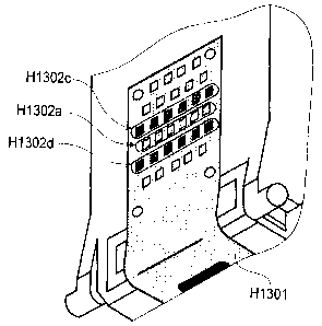
Embodiment 1
CA 02508867 2005-06-O1
23
Referring to Figure 1, the description will be
made as to an ink jet recording head according to the
first embodiment of the present invention..
Figure 1 is an enlarged view of the external
signal input contact portion of the electric wiring
sheet of the second recording head used with the ink
jet recording head of this embodiment: Referring to
Figure 1, the electric wiring sheet H1301 is provided
with 32 external signal input contacts H1302.Of these
to external signal input contacts H1302, six pads are TD
contact pads H1302a which are disposed-substantially
at the central portion of the portion where the
external signal input contacts H1302 are disposed. The
ID contact pads H1302a are respectively connected to
the ID pads connected with the fuse H1117 (a simple
connecting line or the resistance element (Figure
11) ) provided at the opposite ends of each of the
three ink supply ports H1102 of the second recording
element substrate H1101 shown in Figure 10.
2o Six VH contact pads H1302c are disposed along
one side of the array of the ID contact pads H1302a
(the side above the array of the ID contact pads
H1302a in Figure 1) adjacent the ID contact pad H1302a
array. More particularly, in this embodiment, the VH
contact pads H1302c are immediately adjacent to the ID
contact pad H1302a array (namely, with no ID contact
pad H1302a therebetween). These VH contact pads H1302c
CA 02508867 2005-06-O1
24
are electrically connected to the VH pads H.1104c
(Figure 11) provided in the electrode portion H1104
(Figure 10) at the opposite ends of the second
recording element substrate H1101.
Six GNDH contact pads H1302d are arranged along
the array of the ID contact pads H1302a on the other
side, that is, the side below the array of the ID
contact pads H1302a in Figure 1. More particularly, in
this embodiment, the GNDH,contact pads H1302d are
1o immediately adjacent to the ID contact pad H1302a
array (namely, with no ID contact pad H1302a
therebetween). These VH contact pads H1302 d are
electrically connected to the GNDH pads H7.104 (Figure
11) provided in the electrode portion H1104 (Figure
10) at the opposite ends of the second recording
element substrate H1101.
The other external signal input contacts H1302
other than the ID contact pads H1302a, the VH contact
pads H1302c and the GNDH contact pad H1302d, are used
2o for electric power supply to the transistors, sending
and receiving signals such as control signals or the
like.
In the case of the ink jet recording head of
the present invention, the ID contact pads H1302a
which are relative weak against the attach of static
electricity are positioned substantially at the
central portion of the external signal input contact
CA 02508867 2005-06-O1
portion H1302. This position is hard to be touched by
the user, when the user manipulates the second
recording head by hand. Usually, the user is more or
less conscious so as not to touch the external signal
5 input contact H1302, and therefore, the pads disposed
at the center portion is not easily touched.
In addition, the ID contact pads H1.302a are
adjacent to and interposed between the VH contact pad
H1302c and the GNDH contact pad H1302d, and therefore,
to if an electrically charged finger of the user is
brought so close to the ID contact pad H1302a that
electrical discharge occurs, the discharge tends to be
toward the VH contact pad H1302c and/or to the GNDH
contact pad H1302d rather than toward the ID contact
15 pad H1302a. Thus, the. structure of the present
invention is such that peculiar information in the
head is not broken, overwritten or rewritten.
Embodiment 2
Referring to Figure 2, the description will be
2o made as to an ink jet recording head according to a
second embodiment of the present invention.
Figure 2 is an enlarged view of an external
signal input contact portion of electric wiring of a
first recording head usable with an ink jet recording
25 head according to this embodiment. Referring to Figure
2, the electric wiring sheet H1300 is provided with 21
external signal input contacts H1302. The first
CA 02508867 2005-06-O1
26
recording head is for the black ink, and therefore,
the numbers of the electric power supply contacts, the
control signal contacts are smaller than the second
recording head for the cyan, magenta and yellow inks,
as described in the first embodiment.
However, the carriage 102 of the main assembly
of the ink jet recording apparatus is capable of
accepting the third recording head which is for the
photographic printing and which has the same structure
to as the second recording head, at the position where
the first recording head is removed. Therefore, the
positions of the 21 external signal input contacts
H1302 correspond to the positions of the external
signal input contacts H1302 of the_second recording
head when the head is mounted to the carriage 102.
The number of the ID contact pads H1302a of the
external signal input contacts H1302 on the electric
wiring sheet H1300, six, and the positions thereof are
substantially at the center of the portion where the
2o external signal input contacts H1302 are provided. The
ID contact pads H1302a are connected to the ID pads
which in turn is connected to a fuse H1117, a simple
wiring line or a resistance element, Figure 11)
disposed at each of the opposite ends of the ink
supply port H1102 of the first recording element
substrate H1100.
Four VH contact pads H1302c are arranged along
CA 02508867 2005-06-O1
27
and adjacent to the array of the ID contact pad H1302a
at one lateral side (above the array of the ID contact
pads H1302a in Figure 2. More particularly, in this
embodiment, the VH contact pads H1302c are immediately
adjacent to the ID contact pad H1302a array (namely,
with no ID contact pad H1302a therebetween). The VH
contact pads H1302c are connected to the VH pads
H1104c (Figure 11) provided in the electrode portion
H1104 (Figure 7) disposed at the opposite ends of the
to first recording element substrate.
Four GNDH contact pads H1302d are arranged
along and adjacent to the array of the ID contact pad
H1302a at one lateral side (below the array of the ID
contact pads H1302a in Figure 2. More particularly, in
this embodiment, the GNDH contact pads H1302 d are
immediately adjacent to the ID contact pad H1302a
array (namely, with no ID contact pad H1302a
therebetween). The GNDH contact pads H1302d are
connected to the GNDH pads H1104 (Figure 11) provided
2o in the electrode portion H1104 (Figure 7) at the
opposite ends of the recording element substrate H1100.
The other external signal input contacts H1302
other than the ID contact pads H1302a, the VH contact
pads H1302c and the GNDH contact pad H1302d, are used
for electric power supply to the transistors, sending
and receiving signals such as control signals or the
like.
CA 02508867 2005-06-O1
28
According to the ink jet recording head of this
embodiment, similarly to the first embodiment, the ID
contact pads H1302a which axe relative weak against
the attach of static electricity are positioned
substantially at the central portion of the external
signal input contact portion HI302, and therefore, the
user does not easily touch the ID contact pad H1302a.
In addition, the ID contact pads H1302a are
adjacent to and interposed between the VH contact pads
1o H1302c and the GNDH contact pads H1302d, and therefore,
even when if an electrically charged finger of the .
user is brought so close to the ID contact pad H1302a
that electrical discharge occurs, the discharge tends
to be toward the VH contact pad H1302c and/or to the
GNDH contact pad H1302d rather than toward the ID
contact pad H1302a, and therefore, the peculiar
information in the head is not easily broken,
overwritten or rewritten.
Embodiment 3
Referring to Figure 3, the third embodiment
will be described.
Figure 3 is an enlarged view of the external
signal input contact portion of the electric wiring
sheet of the second recording head used with the ink
jet recording head of this embodiment. A second type
recording head of this embodiment uses the second
recording element substrate H1101 which is the same as
CA 02508867 2005-06-O1
29
the first embodiment, and the difference from the
first embodiment is only in the disposition of the
external input contacts H1302 on the external electric
wiring.
Six pads of 32 external signal input contacts
H1302 provided on the electric wiring sheet. H1301 are
ID contact pads H1302a. The ID contact pads H1302a are
arranged in a longitudinal direction (in the direction
of the length of the electric wiring sheet H1301) at
1o the center of the portion where the external signal
input contacts H1302 are provided.
Along the array of the ID contact pads H1302a,
six VH contact pads H1302c are arranged adjacent
thereto at one lateral side thereof, and six GNDH
contact pads H1302d are arranged adjacent thereto at
the other lateral side thereof. More particularly, in
this embodiment, the VH contact pads H1302c are
immediately adjacent to the ID contact pad H1302a
array (namely, with no ID contact pad H1302a
2o therebetween), and the GNDH contact pads H1302 d are
immediately adjacent to the ID contact pad H1302a
array (namely, with no ID contact pad H1302a
therebetween).
According to the ink jet recording head of this
embodiment, similarly to the first embodiment, the ID
contact pads H1302a which are relative weak against
the attach of static electricity are positioned
CA 02508867 2005-06-O1
substantially at the central portion of the external
signal input contact portion H1302, and therefore, the
user does not easily touch the ID contact pad H1302a.
In addition, the ID contact pads H1302a are
5 adjacent to and interposed between the VH contact pads
H1302c and the GNDH contact pads H1302d, and therefore,
even if an electrically charged finger of t:he user is
brought so close to the ID contact pad H1302a that
electrical discharge occurs, the discharge tends to be
1o toward the VH contact pad H1302c and/or to the GNDH
contact pad H1302d rather than toward the ID contact
pad H1302a, and therefore, the peculiar information in
the head is not easily broken, overwritten or
rewritten.
z5 Embodiment 4
Referring to Figure 4, an ink jet recording
head according to a fourth embodiment will be
described.
Figure 4 is an enlarged view of the external
2o signal input contact portion of the electric wiring
sheet of the second recording head used with the ink
jet recording head of this embodiment. A second type
recording head of this embodiment uses th.e second
recording element substrate H1101 which is the same as
25 the first~embodiment, and the difference from the
first embodiment is only in the disposition of the
external input contacts H1302 on the external electric
CA 02508867 2005-06-O1
31
wiring.
Six pads of 32 external signal input contacts
H1302 provided on the electric wiring sheet H1301 are
ID contact pads H1302a. The ID contact pads H1302a are
disposed substantially at the central portion of the
portion where the external signal input contacts H1302
are provided. Around the ID contact pads H1302a (above,
below, left side and right side of the ID contact pads
H1302a in Figure 4), the VH contact pads H1302c and/or
1o the GNDH contact pads H1302d are disposed at positions
adjacent thereto. Each of the ID contact pads H1302a
is are interposed between the VH contact pads H1302c
and the GNDH contact pads H1302d in the longitudinal
direction and in the transverse direction. In other
words, two arrays of three ID contact pads H1302a
extend inclined at the central portion of the portion
where the external signal input contacts H1302 are
provided, and three arrays which comprise six VH
contact pads H1302c and six GNDH contact pads~H1302d
extend so as to interpose the respective ones of the
arrays of the ID contact pads H1302a.
According to the ink jet recording head of this
embodiment, each of the ID contact pads H1302a are
interposed between the VH contact pads H1302c or the
GNDH contact pads H1302d which are disposed around it,
more particularly, at the top, bottom, left and right.
For this reason, the peculiar information in the head
CA 02508867 2005-06-O1
32
of this embodiment is less easily broken, overwritten
or rewritten then in the heads of the other
embodiments. More particularly, in this embodiment,
the VH contact pads H1302c are immediately adjacent to
the ID contact pad H1302a array-(namely, with no ID
contact pad H1302a therebetween), and the GNDH contact
pads H1302 d are immediately adjacent to t:he ID
contact pad H1302a array (namely, with no ID contact
pad H1302a therebetween).
to The ink jet recording head of any of the
foregoing embodiments is not limited to those of the
ejecting types, but is applicable to the ink jet
recording heads of various ink ejecting types.
The external signal input contacts in any of
the foregoing embodiments, may be a pad cannected to
the similar set of pads. As to the ID contact pads,
they may be usable as information writing pads when
the storing element is an information writ.able (not
only readable) element.
2o According to the foregoing embodiments, the
problem of the overwriting or rewriting of individual
information in the storing element due to the static
electricity upon the head mounting, can be solved.
While the invention has been described with
reference to the structures disclosed herein, it is
not confined to the details set forth and this
application is intended to cover such modifications or
CA 02508867 2005-06-O1
33
changes as may come within the purpose of the
improvements or the scope of the following claims.