Note : Les descriptions sont présentées dans la langue officielle dans laquelle elles ont été soumises.
CA 02510501 2005-06-16
2002P18752 WO
Description
Device for Determining the Energy State of an Energy Storing Device of a
Mobile Data
Carrier
The invention relates to a device for determining the energy state of an
energy storing
device of a mobile data carrier. Such a device can be used, for example, in
connection
with contactless identification systems.
Contactless identification systems use contactless transmission techniques,
which can be
based on electromagnetic transmission or transmission using light, infrared or
ultrasound
signals. Systems of this type are used, for example, in transportation
systems, e.g., to
identify persons or moving goods. The necessary data are transmitted by a
transceiver to
a data carrier and back again over a contactless data link, e.g., an air
interface. This
contactless identification method also makes it possible to collect data while
the data
carrier moves past the transceiver, without the need for the data carrier to
be inserted into,
or swiped through a read/write device. Data carriers of this type are used,
for example, as
tickets with an electronically reloadable credit balance, such that the
corresponding
amount is automatically deducted when the means of transport is used.
German Publication DE 691 23 887 T2 discloses an IC card, which can detect a
voltage
drop in the built-in battery. For this purpose, the IC card is equipped with a
data
transceiver, a data processing unit, a charging unit, a comparator and a
timer.
CA 02510501 2005-06-16
2002P18752 WO
German Laid-Open Publication DE 100 54 970 A1 discloses a method for
controlling the
charging and discharging phases of a backup capacitor. In a circuit
configuration, a
constant current source is formed by a current-mirror circuit, and a
comparator is used to
compare the voltage on the backup capacitor with a band gap reference.
To enable the data carriers to be used for an indefinite period of time, the
integration of
chemical energy storing devices, e.g., batteries, is dispensed with in these
units. The
electric power required by the data carriers is instead picked up externally
without
contact, i.e., from a source of energy originating from the transceiver, e.g.,
an electric or
magnetic field. Hence, suitable transmission and coding methods are required
for the
transceiver to communicate with such data carriers. On the one hand only
certain
frequency bands are typically released for the transmission of data, e.g., the
ISM
(Industrial, Scientific & Medical) frequency bands for industrial, scientific
and medical
applications. Possible national radio regulations may define, among other
things,
modulation bandwidths and field strengths to be complied with. On the other
hand, the
transmission and coding methods must also ensure the power supply of the
electronics on
the data Garner.
Such methods are described in ISO/IEC Standard 15693 Part 2, "Air Interface
and
Initialization." Methods of this type enable a continuous power supply of the
data carrier
electronics, which is provided by the energy of the applied carrier frequency
of the
transceiver. To modulate the data to be transmitted, the carrier frequency is
switched off
only for a maximum time interval. Within this time interval, an energy storing
device
previously charged by the electric or magnetic field must be able to supply
the power for
CA 02510501 2005-06-16
2002P18752 WO
the data carrier electronics. The temporary energy storing device used on the
data carrier
is generally a capacitor. The data are coded by switching off the carrier at
defined
positions within a cyclic time-slot pattern. Taking into account the
aforementioned
maximum time interval, the standard further defines the field strength limits
for the
sidebands produced by modulation at a certain carrier frequency. The height of
the
sideband modulation is determined on the one hand by the time ratio of the
switched-on
to the switched-off carrier frequency. In addition, further successive
switching from the
switched-on to the switched-off carrier frequency clearly contributes to the
increase in the
sideband modulation. The need to comply with the sideband limits defined in
the
standard leads to a maximum possible data rate.
Data transmission using contactless transmission methods can be undesirably
influenced,
however, by insufficient coupling. Such insufficient coupling can occur, for
example, if a
mobile data carrier moves very rapidly through a field or moves along the
field
boundaries where the energy transfer is low.
This can have drawbacks, for example, if a write process to a read/write
memory of a
mobile data carrier was started when the coupling between the mobile data
carrier and the
stationary read/write device was sufficient, but because of a movement of the
mobile data
carrier relative to the stationary read/write device, the energy storing
device of the mobile
data carrier cannot be adequately recharged. As a result, the power required
for the write
process may not be available in the mobile data carrier, so that the write
process cannot
be correctly completed.
CA 02510501 2005-06-16
2002P18752 WO
The object of the invention is to provide a way to obviate the above-described
drawbacks.
This object is attained by a device with the features set forth in Claim 1.
Advantageous
embodiments and further refinements of the invention are set forth in the
dependent
Claims 2 - 7. Claim 8 relates to the use of the device according to the
invention in a
mobile data carrier. Claim 9 relates to the use of the device according to the
invention in
an identification system.
The particular advantages of the invention are that information regarding the
energy state
of the mobile data carrier may be provided to the user at any time. This makes
it possible
to determine when the energy state of the energy storing device of the mobile
data carrier
is insufficient and to correctly and completely repeat a data exchange that
was previously
incomplete or faulty because of the insufficient energy state. The means
therefor can be
realized on the mobile data carrier with little additional complexity. A
device according
to the invention provides rapid and accurate information on the energy state
of the energy
storing device of the mobile data Garner. A further advantage of the invention
is that the
received information is almost completely independent of the tolerances of the
involved
circuit elements.
Additional advantageous characteristics of the invention will now be
described, by way
of example, with reference to the figures.
The figures show:
CA 02510501 2005-06-16
2002P18752 WO
FIG 1 a block diagram depicting the essential components of an identification
system necessary to understand the invention,
FIG 2 a circuit diagram depicting a device for determining the energy state of
an
energy storing device of a mobile data carrier,
FIG 3 a diagram illustrating different voltages,
FIG 4 a diagram illustrating the voltage curve of the voltage Ul present at
the
capacitor 7 of FIG 2 as a function of the distance between the read/write
device and the mobile data carrier,
FIG 5 a diagram illustrating the position of two measurement instants,
FIG 6 a diagram illustrating the charging times measured at the first
measurement
instant when a relatively small voltage is present at the capacitor 7, and
FIG 7 a diagram illustrating the charging times as measured at the second
measurement instant when a relatively high voltage is present at the capacitor
7.
FIG 1 shows a block diagram illustrating the essential components of an
identification
system necessary to understand the invention.
The system depicted has a read/write device 1 and a mobile data carrier 4. A
bidirectional
exchange of data D takes place between the read/write device 1 and the mobile
data
carrier 4 over an air transmission link 3. The read/write device further
transmits energy E
to the mobile data carrier 4 over the air transmission link 3. This
transmission of energy
occurs at time intervals when no data are being exchanged. The transmission of
data and
CA 02510501 2005-06-16
2002P18752 WO 6
energy is based on the principle of inductive coupling. For this purpose, the
read/write
device 1 is equipped with a coil 2 and the mobile data carrier 4 with a coil
5.
In the mobile data carrier 4, the transmitted energy is supplied to the energy
storing
device, which is implemented as a capacitor, via a rectifier 6. The
unstabilized DC
voltage present at the capacitor 7 is supplied to a voltage stabilizer 9, at
the output of
which the stabilized DC voltage required to supply the mobile data carrier 4
is made
available.
The capacitor 7 is further connected with a device 8 that is provided for
determining the
energy state of the capacitor 7.
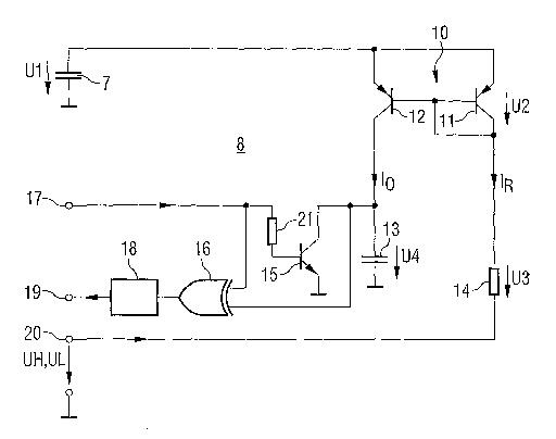
FIG 2 is a circuit diagram showing in greater detail the device 8 for
determining the
energy state of the capacitor 7 of the mobile data carrier 4. The device 8 has
a current
mirror containing transistors 11 and 12. This current mirror has two mutually
parallel
paths. In the first path, in which the transistor 12 is located, a current Io
flows. In the
second path, in which the transistor 11 is located, a current IR flows. In the
second path,
there is also an ohmic resistor 14, which is connected to the transistor 1 l
and the other
terminal of which is connected to a HIGH/LOW level signal input 20 of the
device 8. Via
this input 20, a logic circuit (not depicted) supplies either a HIGH level
signal or a LOW
level signal to the device 8.
In the first path, an auxiliary capacitor 13 is connected to the transistor 12
and with its
other terminal is connected to ground. The terminal of the auxiliary capacitor
13 remote
from the ground is connected to an input of an XOR gate 16 and to the
collector of an
CA 02510501 2005-06-16
2002P18752 WO 7
npn transistor 15. The emitter of the transistor 15 is connected to ground.
The base of the
transistor 1 S is connected to an input 17 of the device 8 via an ohmic
resistor 21. The
input 17 is a measurement time input, which is used to supply signals defining
measurement time intervals to the device 8. These measurement time signals are
generated in the aforementioned logic circuit (not shown), which also supplies
the signals
provided at the HIGH/LOW level signal input 20. This logic circuit has
information on
the system clock, which is required to generate the signals supplied to the
inputs 17 and
20. The measurement time signals present at the input 17 are supplied to the
other input
of the XOR gate 16 and to the base of the npn transistor 15 via the ohmic
resistor 21.
The output signals of the XOR gate 16, which is information regarding the
charging
times of the auxiliary capacitor 13, are supplied to an evaluation logic 18.
The evaluation
logic 18 uses the charging times to calculate a quantity in the form of a
numerical value,
which provides information on the energy state of the capacitor 7. In
particular, this
numerical value contains information regarding the ratio of the unstabilized
supply
voltage present at the capacitor 7 to the stabilized DC voltage required as
the supply
voltage by the mobile data carrier. The latter is, for example, 3 V and is the
operating
voltage of a chip on the mobile data carrier. The information available at the
output of the
evaluation logic 18 can be used, in particular, to make a statement as to how
large the
power reserve of the mobile data carrier is at the time of the measurement.
The mode of operation of the device depicted in FIG 2 will now be described in
greater
detail.
CA 02510501 2005-06-16
2002P18752 WO g
In a current mirror, such as the one realized by the transistors 11 and 12 in
FIG 2, the
following general relation holds:
I" =1- 2 ~1
IR (3+2
Furthermore, for the voltage U of a capacitor C, which is charged with a
constant current
Io, the following relation holds:
U=Io ~ t/C
Converting this relation yields:
t = U ~ C / Io (Equation 1 )
These relations also hold for the charging process of the auxiliary capacitor
13 and are
taken into account when the energy state of the capacitor 7 is determined
according to the
invention.
If according to FIG 2 the dropping voltage at the capacitor 7 is Ul, the
dropping voltage
at the transistor 11 is U2, the dropping voltage at the resistor 14 is U3 and
the voltages
provided at the input 20 are UH and UL, respectively, the following holds:
U3 = U 1 - U2 - UL, if UL is present at the input 20, and
U3 = U 1 - U2 - UH, if UH is present at the input 20.
If UL = 0, then:
U3=U1-U2
The following relation holds for the current IR if UH is present at the input
20:
CA 02510501 2005-06-16
2002P18752 WO
_ U3-UH
IR(UH)
R,a
If UL is present at the input 20 the following holds for current IR:
U3-UL
IR(~.) _
R"
For UL = 0:
IR(UL) _ U3 (Equation 2)
IR(UH) U3-UH
Consequently, when the quotient of the currents IR(UL) and IR~UH> is formed
the value of
the resistor 14 is eliminated.
Taking into account equations 1 and 2, the following relations are obtained
for the device
shown in FIG 2:
C" ~ U4
t=
Io
Io ~ IR
_C"~U~,
tUFi I
R(UH)
_C"~U",
tUL I
R(UL)
Hence:
tUli = IR(UL) __ U3 (Equation 3)
t~~ IR(UH) U3-UH
tUH and tug are the charging times of the auxiliary capacitor 13 if this
capacitor is charged
by the currents IR~uH~ or IR~uL> until the voltage threshold value Ut,, is
reached at the input
CA 02510501 2005-06-16
2002P18752 WO 10
of the XOR gate. The assumed input condition was that the auxiliary capacitor
13 is
completely discharged via the conducting transistor 15 prior to the start of a
measurement
process, as will be explained below with reference to FIG 6 and 7.
Equation 3 shows that neither the capacitance value of the auxiliary capacitor
13 nor the
voltage value of the threshold voltage Uth influences this equation. The
charging times
tUH and tUL are inversely proportional to the charging currents IR~UH~ and
IR(UL)~
The effective application range of equation 3 is the range of UH « U3 and U3 -
UH > 0.
FIG 3 is a diagram illustrating various voltages of FIG 2. The distance S of
the read/write
device 1 from the mobile data carrier 4 is plotted along the abscissa and the
inductive
coupling or the coupling factor k along the ordinate. It is clear that the LOW
level signal
UL and the HIGH level signal UH are each constant, independent of the distance
S, and
that the voltage U1 present at the capacitor 7 becomes smaller with increasing
distance S.
The supply voltage of the mobile data carrier 4 is obtained from the
unstabilized voltage
U 1 present at the capacitor 7 through a stabilization taking place in circuit
block 9 of FIG
1. It is assumed that the following relations hold in the low-load state:
UL~OV
UH ~ UCHIP~
where U~HIP is the supply voltage of the mobile data carrier 4.
CA 02510501 2005-06-16
2002P18752 WO 11
FIG 4 shows a diagram illustrating the voltage curve of the unstabilized
voltage U 1
present at the capacitor 7 of FIG 2 as a function of the distance between the
read/write
device 1 and the mobile data carrier 4. This bell-shaped voltage curve is
present even if
the mobile data carrier 4 is moved parallel to the read/write device 1 at a
constant
distance.
FIG 5 is a diagram illustrating the position of two measurement instants or
measurement
time intervals. If the mobile data carrier 4 is moved parallel to the
read/write device 1 at a
constant distance S, then the voltage U 1 at the capacitor 7 has the time
characteristic
shown, which is bell-shaped. According to the invention, two arbitrary
measurement
instants or measurement time intervals are determined, such that the voltage
value is
relatively small at the measurement instant tl and relatively large at the
measurement
instant t2. During the time intervals defined by the measurement points, the
voltage curve
is measured at the auxiliary capacitor 13. As may be seen from FIG 6 and 7,
different
charging times result at the measurement points, making it possible to draw
conclusions
regarding the energy state of the capacitor 7 of the mobile data carrier 4 and
thus also
regarding the operability of the mobile data carrier 4.
FIG 6 shows a diagram illustrating the measured charging times as measured at
the first
measurement instant tl, at which a comparatively small voltage U1 is present
at the
capacitor 7. The trace (a) of FIG 6 represents the signal UH or UL applied to
the input 20,
the trace (b) represents an integration time signal, the trace (c) represents
the
measurement time signal applied to the input 17, the trace (d) represents the
threshold
voltage Ut,, and the trace (e) the voltage U4 present at the auxiliary
capacitor 13.
CA 02510501 2005-06-16
2002P18752 WO 12
The signal UH or UL represented in the trace (a) and the measurement time
signal
represented in the trace (c) are predefined by the logic circuit (not shown)
in which
information on the system clock is available. The measurement time signal is
started
when the signal shown in the trace (a) passes from the HIGH to the LOW state.
The
integration time interval shown in the trace (b) also starts at this instant.
As shown in the
trace (e) the charging of the auxiliary capacitor 13 by charging current
Ip(UL) likewise
starts at this instant. The charging process is continued until the voltage at
the auxiliary
capacitor 13 reaches the threshold voltage U~, shown in the trace (d). At this
instant-as
indicated in the trace (bathe integration time is terminated and provided to
the
evaluation logic 18 as charging time tUL. After this instant, the measurement
time interval
is terminated as may be seen from the trace (c). Immediately after the end of
the
measurement time interval, the auxiliary capacitor 13 is discharged by the
transistor 15,
which is then conducting.
When the HIGH/LOW level signal shown in the trace (a) is at the HIGH level and
the
auxiliary capacitor 13 is discharged, a second measurement time interval is
started-as
indicated by the second falling edge of the measurement time signal depicted
in the trace
(c). At this instant, a new measurement of the integration time is started as
indicated by
the second rising edge of the integration time signal depicted in the trace
(b). The
charging of the auxiliary capacitor 13 by charging current Ip(UH) is also
started at this
instant. The charging process is continued until the voltage at the auxiliary
capacitor 13
reaches the threshold voltage Uth shown in the trace (d). At this instant-as
shown in the
trace (b)-the integration time is terminated and provided as the charging time
tUH to the
evaluation logic 18. If at this instant the measurement time signal returns to
the HIGH
CA 02510501 2005-06-16
2002P18752 WO 13
state, this measurement time interval is likewise terminated and the auxiliary
capacitor 13
is discharged via the transistor 15, which is then conducting.
FIG 7 shows a diagram illustrating the measured charging times as measured at
the
second measurement instant t2 at which a relatively large voltage U1 is
present at the
capacitor 7. The trace (a) of FIG 7 represents the signal UH or UL applied to
the input 20,
the trace (b) represents an integration time signal, the trace (c) represents
the
measurement time signal applied to the input 17, the trace (d) represents the
threshold
voltage Uth and the trace (e) the voltage U4 present at the auxiliary
capacitor 13.
The signal UH or UL represented in the trace (a) as well as the measurement
time signal
represented in the trace (c) are predefined by the logic circuit (not
depicted), in which
information on the system clock is available. The measurement time signal is
started
when the signal shown in the trace (a) passes from the HIGH to the LOW state.
At this
instant, the integration time interval shown in the trace (b) also starts. As
shown in the
trace (e), the charging of the auxiliary capacitor 13 by the charging current
Ip(UL) likewise
starts at this instant. The charging process is continued until the voltage at
the auxiliary
capacitor 13 reaches the threshold voltage Uth shown in the trace (d). At that
instant-as
indicated in the trace (b)-the integration time is terminated and provided as
charging
time tU~ to the evaluation logic 18. After this instant, the measurement time
interval is
terminated, as indicated in the trace (c). Immediately after the end of the
measurement
time interval, the auxiliary capacitor 13 is discharged through the transistor
15, which is
then conducting.
CA 02510501 2005-06-16
2002P18752 WO 14
If the HIGH/LOW level signal shown in the trace (a) is at the HIGH level and
the
auxiliary capacitor 13 is discharged, a second measurement time interval is
started-as
indicated by the second falling edge of the measurement time signal shown in
the trace
(c). At this instant, a new measurement of the integration time starts as
indicated by the
second rising edge of the integration time signal shown in the trace (b).
Charging of the
auxiliary capacitor 13 by the charging current Io~uH~ likewise starts at that
instant. The
charging process is continued until the voltage at the auxiliary capacitor 13
reaches the
threshold voltage Ut,, shown in the trace (d). At this instant as shown in the
trace (b)-
the integration time is terminated and provided to the evaluation logic 18 as
the charging
time tUH. If after this instant the measurement time signal returns to the
HIGH level, this
measurement time interval is likewise terminated and the auxiliary capacitor
13 is
discharged via the transistor 15, which is then conducting.
The evaluation logic 18 forms the quotient of the charging times tUL and tUH
and provides
this quotient as the quantity describing the energy state of the capacitor 7
at the output 19
of the device 8. From there this quantity is supplied to a transmission unit
of the mobile
data carrier 4 and is transmitted to the read/write device 1 over the air
transmission link 3.
There it is available for display, by means of which a user can assess the
energy state of
the capacitor 7 of the mobile data carrier 4 and take suitable measures if
required. As an
alternative thereto, the quantity describing the energy state of the capacitor
7 transmitted
to the read/write device 1 can also be evaluated by an automatic unit in the
read/write
device 1, which introduces suitable measures automatically if necessary.