Note : Les descriptions sont présentées dans la langue officielle dans laquelle elles ont été soumises.
CA 02512358 2005-07-15
Docket No. 02-1-826 PATENT APPLICATION
METHOD AND CIRCUIT FOR IGNITING AND POWERING
A HIGH INTENSITY DISCHARGE LAMP
Ronald M. Fiorello
FIELD OF THE INVENTION
[0001] The present invention generally relates to circuits for powering
discharge
lamps, and more particularly to a method and circuit for igniting and powering
a high
intensity discharge lamp.
BACKGROUND OF THE INVENTION
[0002] In starting a high intensity discharge (HID) lamp, the lamp experiences
three
phases. These phases include breakdown, glow discharge, and thermionic arc.
Breakdown requires a high voltage to be applied between the electrodes of the
lamp.
Following breakdown, the voltage must be high enough to sustain a glow
discharge and
heat the electrodes to thermionic emission. Once thermionic emission
commences,
current must be maintained in the run-up phase until the electrodes reach
steady-state
temperature. After achieving the arc state, the lamp can be operated with a
lower level of
current in the steady state operating mode.
[0003] For ignition of the lamp, the lamp electrodes must be provided with a
high
voltage for a specified duration in the pre-breakdown period. Conventional
lamps are
characterized by a minimum voltage level and time duration in achieving
breakdown.
HID lamps require a high ignition voltage (e.g., 1000 to 5000 V«"S) to
initiate the plasma
discharge when cold. Lamp input power is typically 5-10 times higher during
lamp
ignition than the rated steady state lamp power because of high transient
power losses.
This voltage creates a high intensity electrical field applied to the
electrodes that initiates
the discharge. The high voltage requirements for breakdown can be achieved
through
pulse resonant circuits. The frequency at which the circuit achieves resonance
and the
resultant resonant voltage varies from circuit to circuit due to variation in
component
tolerances. Because lamp starting voltage depends on inverter input voltage,
it is
CA 02512358 2005-07-15
Docket No. 02-1-826 PATENT APPLICATION
important that the DC bus voltage is maintained by keeping it in a definite
range as long
as possible before the lamp ignites.
[0004] However, the stress on a ballast during ignition can be significant.
This is
especially true with regard to a power transistor within a flyback converter.
That is, there
is a voltage stress on the primary side power transistor during ignition
because the
voltage reflected back to the power transistor is proportional to the ratio of
the primary
and secondary windings (Np/Ns) of the flyback transformer. Accordingly, there
is a need
for a ballast which provides reduced stress on the power transistor during
ignition.
[0005] Once the arc has been established, it is beneficial to provide a
constant power
to the lamp to assure a constant and relible light output. Typically,
electronic ballasts
regulate lamp power when operating high intensity discharge lamps by sensing
the lamp
current and the lamp voltage. The sensed lamp current and voltage are
multiplied to get
the wattage. The multiplication could be achieved using a micro-controller or
microprocessor. The wattage is then compared to a reference wattage. A
feedback loop is
provided in such a way that the error that resulted from this comparison is
converted to a
signal adjusting the lamp current so that the measured lamp power is equal to
the
reference power.
[0006] Prior art electronic ballasts for HID lamps receive an alternating line
current,
such as the alternating line current provided by a voltage source 10 as shown
in Fig. 1.
The current is provided to a rectifier circuit 12, which generates an output
to a boost
converter 14. The boost converter is typically controlled by a power factor
correction
controller 16. The boost converter typically has it own voltage control loop
to maintain
its output voltage higher than the input voltage. The boost converter is then
followed by a
power processing stage comprising a DC-DC converter 18, such as a buck
converter or
other suitable type of DC-DC converter, that again has its own control loop,
such as a
pulse width modulation (PWM) controller 20, and is used to maintain a constant
voltage
or current output and to perform the necessary voltage conversion and
conditioning. The
power processing stage is coupled to an inverter 22 (controlled by a
corresponding
inverter driver circuit 24) which delivers power to the lamp 26.
2
CA 02512358 2005-07-15
Docket No. 02-1-826 PATENT APPLICATION
[0007] However, the power processing stage results in additional power losses
as
well as additional components which lead to increased size and higher cost. In
manufacturing electronics generally, any reduction in the necessary parts can
be
significant. In the field of electronic ballasts, any improvement which can
reduce material
cost is significant. For example, the reduction or elimination of conventional
circuitry
can reduce part count and reduce cost significantly. Therefore, a need exists
for a ballast
that does not require a separate power processing stage in order to regulate
the power that
is supplied to an HID lamp.
OBJECTS OF THE INVENTION
[0008] It is an object of the present invention to provide a universal input
voltage
electronic ballast to reliably regulate lamp power from a power factor
corrected (PFC)
flyback converter stage, which eliminates any need for a separate DC-DC
converter
power processing stage and avoids its associated energy losses, size, weight
and cost.
[0009] It is a further object of the present invention to provide a
microprocessor
control circuit arrangement for programmable start of a universal voltage
electronic
ballast having an active flyback, power regulated power factor corrector and
an inverter.
[0010] It is another object of the present invention to provide a
microprocessor
control circuit arrangement for programmable start of a universal voltage
ballast having
an additional winding on the flyback transformer to provide the necessary open
circuit
voltage to ignite the lamp.
[0011] It is another object of the present invention to provide a
microprocessor
control circuit arrangement for average power regulation and programmable
start of a
universal voltage ballast having an additional winding flyback transformer for
open
circuit voltage, an active flyback, power regulated power factor corrector and
an inverter.
[0012] Accordingly, it is desirable to provide an improved electronic ballast
for
igniting and regulating power in a high intensity discharge lamp.
3
CA 02512358 2005-07-15
Docket No. 02-1-826 PATENT APPLICATION
SUMMARY OF THE INVENTION
(0013] A circuit for igniting and powering a high intensity discharge lamp is
disclosed. The circuit according to one embodiment of the invention comprises
a rectifier
circuit coupled to receive an alternating current line voltage. A flyback
converter
coupled to the rectifier circuit has a flyback transformer comprising a
primary inductive
winding, a secondary inductive winding, and a supplemental inductive winding.
An open
circuit voltage circuit coupled to the secondary inductive winding couples the
supplemental inductive winding to the secondary winding during ignition of the
lamp.
(0014] A method of igniting and powering a high intensity discharge lamp is
also
disclosed. The method comprises the steps of generating a DC voltage for the
high
intensity discharge lamp by way of a flyback converter; providing a flyback
transformer
comprising a primary inductive winding, a secondary inductive winding, and a
supplemental inductive winding in the flyback converter; and coupling the
supplemental
inductive winding to the secondary winding during ignition.
4
CA 02512358 2005-07-15
Docket No. 02-1-826 PATENT APPLICATION
BRIEF DESCRIPTION OF THE DRAWINGS
[0015] Fig. 1 is a block diagram of a conventional circuit for igniting and
powering a
high intensity discharge lamp;
[0016] Fig. 2 is a block diagram of circuit for igniting and powering a high
intensity
discharge lamp, according to an embodiment of the present invention;
[0017] Fig. 3 is a more detailed block diagram of the circuit of Fig. 2,
according to an
embodiment of the present invention;
[0018] Fig. 4 is a detailed circuit diagram of a rectifier circuit, a flyback
converter,
and a flyback control circuit, according to an embodiment of the present
invention;
[0019] Fig. 5 is a detailed circuit diagram of an inverter and inverter driver
circuit,
according to an embodiment of the present invention;
[0020] Fig. 6 is a detailed circuit diagram of a power control circuit,
according to an
embodiment of the present invention;
[0021] Fig. 7 is a diagram that descrined the shaping of a sinusoidal input
current,
according to an embodiment of the present invention;
[0022] Fig. 8 is a flow diagram showing a method of igniting and powering a
high
intensity discharge lamp, according to an embodiment of the present invention;
and
[0023] Fig. 9 is a flow diagram showing a method of igniting and powering a
high
intensity discharge lamp, according to an alternate embodiment the present
invention.
CA 02512358 2005-07-15
Docket No. 02-1-826 PATENT APPLICATION
DETAILED DESCRIPTION OF THE PREFERRED EMBODIMENTS
The various embodiments of the present invention relate to an electronic
ballast
and method for igniting and powering a high intensity discharge lamp from a
universal
input AC line voltage. The present invention includes an active power factor
corrector
circuit configured as a flyback converter to provide power factor correction
and power
regulation in a single power processing stage. Average lamp power is regulated
by a
micro-controller driving a Transition Mode (TM) or critical conductance mode
power
factor controller. The output current and voltage of the flyback converter are
varied to
regulate the lamp power. Either the DC output bus power can be regulated, or
with the
addition of a current and voltage transformer, the inverter AC output power
can be
regulated. Because the average is taken of a digital PWM output voltage based
on a
table lookup and is used to regulate the power of the flyback converter, the
need for an
intermediate DC-DC converter stage and its associated cost and size are
eliminated.
Thus, the single stage, single switch flyback converter provides both power
factor
correction and load power regulation.
Additionally, the present invention provides a supplemental winding on a
flyback transformer in order to ignite the lamp with lower stress on the
components of
the flyback converter. The additional winding on the flyback transformer
generates the
necessary open circuit voltage for the lamp. The additional winding reduces
the voltage
stress on the primary side power switch during ignition since the voltage
reflected back
to the primary is proportional to the ratio of Np/Ns of the flyback
transformer. The
additional winding is switched out of the circuit by the micro-controller once
ignition of
the lamp occurs.
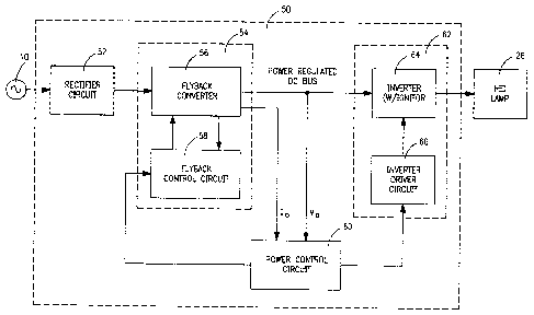
(0024] Turning to Fig. 2, a block diagram of a circuit for igniting and
powering a
high intensity discharge lamp according to an embodiment of the present
invention is
shown. The circuit is used to regulate HID lamps powered from a source 10 such
as a
120 or 277 V AC line, for example. In particular, an electronic ballast 50 for
energizing
an HID lamp 26 comprises a rectifier circuit 52 coupled to an AC line source
10 and an
active power factor corrector circuit 54. The active power factor corrector
circuit 54
6
CA 02512358 2005-07-15
Docket No. 02-1-826 PATENT APPLICATION
comprises a single stage, single switch converter configured as a flyback
converter 56
providing AC-DC conversion and a flyback control circuit 58, providing power
factor
correction and power regulation in a single power processing stage. An
inverter section
62 comprises an inverter circuit 64 having an igniter and receiving the output
of the
flyback converter 56 by way of a power regulated DC bus, and an inverter
driver circuit
66. As will be described in more detail below, the inverter circuit 64
provides the
necessary voltage to ignite and power the HID lamp.
[0025] A single loop power regulation method according to an embodiment of the
present invention is employed to maintain constant power to the lamp. The
various
connections between the circuits of Fig. 4-6 are shown in more detail in Fig.
3 to enable
an understanding of the interaction between the various circuits. As will be
described in
more detail in reference to Fig. 4, the power factor corrector circuit 54
feeds an inverter
to provide AC excitation to drive an HID lamp. The inverter circuit 64 and the
inverter
driver circuit 66 will be described in more detail in reference to Fig. 5.
Finally, the power
control circuit 60 detects the current and voltage output by the flyback
converter 56, as
will be described in more detail in reference to Fig. 6.
[0026] Turning now to Fig. 4, a circuit diagram of the active power factor
correction
circuit according to an embodiment of the present invention is shown. The
circuit, which
is generally an AC to DC converter section, comprises a rectifier circuit 52
having diodes
D2-DS and a capacitor C4 coupled across the output of the rectifier circuit
52. The
flyback converter 56 coupled to the rectifier circuit comprises a flyback
transformer
having windings Ll-L3. A capacitor C17 is coupled between the node at the L1
winding
and transistor Q 1 and ground. A power switching transistor Q 1 is driven via
an input
resistor R54 to periodically energize the flyback transformer inductor Ll from
a rectified
voltage. An output rectifier diode D6 is connected to the secondary winding L2
of the
flyback transformer. An output energy storage capacitor C2 is coupled across
the output
of the flyback circuit. According to one embodiment of the present invention,
the
windings of the conductors are configured such that the L1 to L2 turn ratio is
1 to 0.65,
7
CA 02512358 2005-07-15
Docket No. 02-1-826 PATENT APPLICATION
where L 1 has 30 turns, the L 1 to L3 turn ratio (zero current winding) is 1
to 0.15, and L 1,
L2, and L3 are wound on TDK PQ40/40 cores.
[0027] An open circuit voltage circuit comprising a supplemental winding L4 is
coupled to winding L2 by a switch S 1. The supplemental winding L4 is coupled
in series
with a diode D10 and a resistor R30. The supplemental winding L4 preferably
has twice
the number of turns of L2. Switch S 1 may be implemented by a relay or an
isolated
semiconductor switch, for example. Switch S 1 is closed prior to ignition of
the lamp to
couple winding L4 in series with winding L2, and then is opened after ignition
to
decouple winding L4 from winding L2. Switch S 1 may be controlled by the
microprocessor U101 (see Fig. 6), for example, receiving a signal from pin 27
of U101.
That is, a coil LS coupled between +5 volts and U 1 O 1 pin 27 opens or closes
switch S 1 in
dependence on the signal provided at U 1 O 1 pin 27. The flyback section of
the power
factor corrector circuit preferably operates in the critical conduction mode
to minimize
switching losses, and incorporates a Transition Mode (TM) controller
regulating a
constant output power via a micro-controller commanded reference.
[0028] The flyback converter 56 is also coupled to the flyback control circuit
58
which comprises a power factor controller circuit having a power factor
controller U 1 S,
such as an SGS Microelectronics L6561 TM controller. The power factor
controller U15
is provided with a voltage feedback loop through a resistor divider R60-R62, a
current
feed back loop through resistor R63, and a power regulation loop. The resistor
divider
network comprising resistors R60, R61 and R62 generates a voltage associated
with the
open-circuit output of the flyback converter 56. A second resistor network
comprising
resistors R69, R70, R71 and R41 generates a feedback current signal at output
210 and a
feedback voltage signal at output 212. As will be described in more detail in
reference to
Fig. 6, the feedback voltage and feedback current signals are coupled to the
power control
current 60 to generate a power control signal which is fed back by way of a
power control
loop to the power factor controller U15. Based upon the value of the power
control
signal, the power factor controller regulates the power of the flyback circuit
56 after
ignition by controlling the frequency and the duty cycle at which transistor Q
1 is driven.
8
CA 02512358 2005-07-15
Docket No. 02-1-826 PATENT APPLICATION
[0029] The AC to DC converter section shapes the sinusoidal input current to
be in
phase with sinusoidal input voltage and regulates the output power of the
flyback
converter through the power command control loop coupled to the power
transistor Q 1
by way of a resistor 854. The power factor controller circuit U15 is
preferably provided
with a peak current sense feature for zero current turn-on and near zero
voltage turn-off
of the power transistor. A resistor network comprising resistors 866, 867 and
868
provides the voltage at the input of the flyback converter to the power factor
controller
U15. A small ceramic capacitor C9, such as a 0.1 uF capacitor, is preferably
coupled to
pin 3 of U15 to reduce noise at that pin. A resistor/capacitor circuit
comprising 865 and
C22 is coupled to the rectifier circuit output 106,108 and generates a bias
during start-up
of the lamp to provide an auxiliary supply to U15 until the lamp lights. A 0.1
of
capacitor C8 is preferably coupled to pin 8 of U15 to reduce noise at that
pin. According
to one embodiment of the invention, Q1 is an IXS24N100 24A/1000V power
transistor
from IXYS Corporation. 841 is a 2W, 5% resistor comprising four 0.62 ohm
resistors in
parallel. D10 is a 8A/600V diode from IXYS Corporation. The remaining
capacitors,
resistors, and diodes preferably have the following values set forth in Table
1.
TABLE 1
Component Value
C4 .22uf/SOOV
C 17 560uF/350V
C2 470uF/400V
C22 22uF/SOV
C23 1 uF/50
V
C21 2200pF/
I kV
D2,3,4,5 3A/600V
854 22ohms
863 .1 Sohms
864 34k ohms
860,61 124k ohms
862 2.49k ohms
866,67 750k ohms
868 9.1k ohms
865 150k ohms
869,70 250k ohms
871 Sk ohms
9
CA 02512358 2005-07-15
Docket No. 02-1-826 PATENT APPLICATION
[0030] Turning now to Fig. 5, a circuit diagram of the inverter circuit 64 and
the
inverter driver circuit 66 according to an embodiment of the present invention
is shown.
In particular, a typical igniter circuit comprises a resistor R20, a capacitor
C20, an
inductor L20-L21, and a spark gap generator G1. The igniter circuit is coupled
across the
lamp to ignite the lamp, as is well known in the art. Inverter driver circuit
66 includes
gate drivers U16 and U17, each of which preferably comprises an IR2101 gate
driver
from International Rectifier. The gate drivers U16 and U17 control transistors
M2 and
M4 and transistors M3 and M5, respectively, which comprise an H bridge
converter for
converting the DC voltage generated by the flyback converter 56 to an AC
voltage.
Preferably, transistors M2, M3, M4, and MS are 12A/600V transistors, such as
20N60S
transistors from Infineon Corporation. Capacitors C24 and C25 are luF/SOV
capacitors,
diodes D36 and D37 are lA/600V diodes, and resistors R55-58 are 22 ohm
resistors.
[0031] Turning now to Fig. 6, a block diagram of a power control circuit
according to
an embodiment of the present invention is shown. The power control circuit
preferably
comprises a microprocessor, such as a Microchip PIC 18C242 or similar micro-
controller, and includes a first input terminal 802 for monitoring the output
current (via
resistor R53 of Fig. 4) of the flyback converter 56, and a second input
terminal 804 for
monitoring the DC bus voltage (via resistive divider R69, R70, R71 of Fig. 4)
at the
output of the flyback converter. The first input terminal is coupled to a
differential OP-
AMP U125A, gain setting resistors 8105, 8106, 8107, 8108, and frequency
compensation capacitor C 109. The first input terminal enables a single stage,
single
switch power factor corrected AC-DC converter and constant average lamp power
that is
scalable to other power levels via the proper adjustment of 8105, 8106, 8107
and 8108
or via a change in look-up table ROM values. A second input terminal 804 is
coupled to
coupled to OP-AMP U125B, gain setting resistors 8109, 8110, 8111, 8112, and
frequency compensation capacitor C 110. The output of the microprocessor U 101
is
coupled to a current amplifier comprising OP-AMP U122A. In particular, U122A
is
driven by the U101 by way of diodes D102 and D103, which are preferably 1N4148
diodes, until the lamp lights, when the power regulation circuit takes over.
An associated
CA 02512358 2005-07-15
Docket No. 02-1-826 PATENT APPLICATION
low pass filter comprising 8139, C126, 8140 and C125 is also coupled to the
other input
of OP-AMP 122A to provide power regulation. The duty cycle of the signal at
pin 13 of
U101, which is based upon the output voltage at the output of U125B coupled to
pin 2 of
U101, is based upon the values in a lookup table as depicted in Table 2 below.
TABLE 2
Output Volts Dut,~,
1.310484 0.66129
1.315249 0.65927
1.320015 0.65726
1.324780 0.65524
1.329545 0.65323
1.334311 0.64919
1.339076 0.64718
1.343842 0.64516
1.348607 0.64315
1.353372 0.64113
1.358138 0.63911
1.362903 0.63710
1.367669 0.63508
1.372434 0.63105
The low pass filter couples an average value voltage to pin 3 of U122A. The
output of
the OP-AMP 122A is fed back (via output 810) to the flyback control circuit
58, which
controls the frequency and duty cycle that transistor M1 is turned on based
upon the
value of the output of OP-AMP 122A. That is, the output of OP-AMP 122A
comprises a
power control signal which controls the power generated by the flyback
converter.
[0032] It should be noted that the lamp current and voltage which are used to
regulate
the lamp power are monitored by microprocessor U101 (Fig. 6) to detect any
fault
conditions that may occur. If a fault condition does occur, the microprocessor
sends a
command (by way of diode D 102, OP-AMP U 122A, and output 810) to effectuate
shutdown of the flyback converter, thus providing protection for the ballast
electronics.
Preferably, the resistors and capacitors in the circuit of Fig. 6 have the
following values:
8101,103,104 = l k ohm, 8105,108 = 25k ohm, 8106,107,110,111,139,140 = l Ok
ohm,
8109,112 = 39.2k ohm, 8133 = 40k ohm, 8142,146 = Sk ohm,
C 1 O 1,102,124,125,126,134,139 = 1 uF, C 103,104 = 18 pF, C 109,110 = 470 pF.
11
CA 02512358 2005-07-15
Docket No. 02-1-826 PATENT APPLICATION
[0033] Turning now to Fig. 7, a block diagram describes the shaping of a
sinusoidal
input current according to an embodiment of the present invention. An embedded
micro-
controller, such as U101 of Fig. 6, measures lamp power by sampling lamp
voltage and
current. The voltage is used as an index into a look-up table to determine the
appropriate
current command to arrive at the correct lamp power. The micro-controller
provides a
digital pulse width modulated output whose duty ratio is proportional to the
measured
lamp voltage. This signal is then averaged and used as the reference for the
current error
amplifier, for example OP-AMP 122A of Fig. 6. That is, the summer blocks and
error
amplification could be performed by OP-AMP 122A which receives Vree at pin 3
and
outputs a power control signal V~ representing an error signal. The output V~
of this error
amplifier is used instead of the error amplifier internal to a power factor
controller as a
variable input to the multiplier. This input is multiplied by a sample of the
rectified line
voltage to provide a rectified AC reference. The reference is compared to the
power
switch current to shape sinusoidal input current such that the input current
is I;~=
K*sinwt, where K is the variable DC term controlled by the power control loop.
The
multiplication and pulse width modulation could be performed by the power
factor
controller U15, which receives the sensed peak voltage Vp and outputs a duty
cycle signal
"d" coupled to the flyback converter. The output current Io is then modified
by an
amplification factor K2 to generate a voltage input VS to U122A. The power
factor
controller voltage amplifier provides a regulated open circuit bus voltage of
approximately 300VDC before lamp ignition is initiated. Once lamp ignition has
occurred, the power regulation loop controls and regulates lamp power based on
a lookup
table stored in onboard program ROM.
[0034] Turning now to Fig. 8, a flow diagram shows a method for igniting and
powering a high intensity discharge lamp according to an embodiment of the
present
invention. In particular, an alternating current is received at a rectifier
circuit at a step
802. A DC voltage is generated for a high intensity discharge lamp by way of a
flyback
converter at a step 804. An inductive winding comprising a primary inductive
winding
and a secondary inductive winding in the flyback converter is provided at a
step 806. A
12
CA 02512358 2005-07-15
Docket No. 02-1-826 PATENT APPLICATION
supplemental inductive winding is coupled to the secondary winding during
ignition at a
step 808. The high intensity discharge lamp is ignited at a step 810. The
supplemental
winding is decoupled after igniting the high intensity discharge lamp at a
step 812. The
power output by the flyback converter is modified to regulate power to the
lamp based
upon the voltage and the current at a step 814.
[0035] Turning now to Fig. 9, a flow diagram shows a method for igniting and
powering a high intensity discharge lamp according to an alternate embodiment
the
present invention. In particular, an alternating current is received at a
rectifier circuit at a
step 902. An inductive winding comprising a primary inductive winding and a
secondary inductive winding is provided at a step 904. A supplemental
inductive
winding is coupled to the secondary winding during ignition at a step 906. The
high
intensity discharge lamp is then ignited at a step 908. The supplemental
winding is
decoupled after igniting the high intensity discharge lamp at a step 910. A
pulse width
modulated output of a flyback converter coupled to the high intensity
discharge lamp is
generated at a step 912. A voltage generated by the flyback converter is
detected at a step
914. A feedback current is then compared with a reference current of the pulse
width
modulated output at a step 916. It is then determined whether the power
provided to the
lamp is correct at a step 918. If not, a power control signal is coupled to
the flyback
converter at a step 920. The output power of the flyback converter is modified
by way of
the power control signal at a step 922.
[0036] It can therefore be appreciated that a new and novel circuit and method
for
igniting and operating a high intensity discharge lamp has been described. It
will be
appreciated by those skilled in the art that numerous alternatives and
equivalents will be
seen to exist which incorporate the disclosed invention. As a result, the
invention is not
to be limited by the foregoing embodiments, but only by the following claims.
I Claim:
13