Note : Les descriptions sont présentées dans la langue officielle dans laquelle elles ont été soumises.
CA 02512845 2005-07-08
WO 2004/064120 PCT/US2004/000621
SEMICONDUCTOR PACKAGE HAVING NON-CERAMIC BASED
WINDOW FRAME
Background of the Invention
1. Field of the Invention
The present invention relates to semiconductor packages, and more
particularly to packages in which one or more dies are mounted on a flange
within an opening in a window frame mounted on the flange and having leads
mounted thereon.
2. History of the Prior Art
It is known in the art to provide semiconductor packages in which one or
more semiconductor dies are mounted on a heat sink flange within an opening
in a window frame which mounts and insulates a plurality of leads. The dies
may be of the LDMOS (lateral diffusion metal oxide semiconductor) type and
the package of the type for packaging LDMOS power transistors. The window
frame, which is typically made of ceramic based materials such as alumina,
serves to mount the leads on the semiconductor package and insulate the leads
from the heat sink flange and other portions of the package. The window frame
has an opening therein which surrounds the semiconductor dies. The dies are
electrically coupled to the conductors such as by wire bonds.
In semiconductor packages of the type described, the components parts
thereof, including the flange, the window frame and the leads, are joined
together such as by brazing/soldering to form a header. One or more dies are
then mounted such as by brazing/soldering/adhering to the header and are
electrically attached to the leads such as by wire bonding. During assembly of
the header, the semiconductor package is typically subjected to very high
temperatures on the order of 700-900°C in order to carry out brazing.
Such
high temperatures dictate that the materials being joined, including
particularly the heat sink flange and the window frame, have similar
coefficients of thermal expansion (CTE). Ideally, the flange is made of highly
conductive materials such as copper. However, because the alumina or other
ceramic materials of the window frame has a much lower rate of thermal
CA 02512845 2005-07-08
WO 2004/064120 PCT/US2004/000621
expansion, it is often necessary to make the flange of less conductive
material
having a closer CTE match to the ceramic material of the window frame.
Without such a close CTE match, the flange and the window frame expand and
contract at substantially different rates so as to place substantial stresses
on
the package. Complicating such situations is the brittle nature of the ceramic
material of the window frame, causing it to break or otherwise fail as a
result of
such stresses.
It would therefore be desirable to provide a semiconductor package
allowing for the use of highly conductive materials such as pure copper for
the
heat sink flange. The material of the window frame should provide a close CTE
match with the flange, and should ideally be flexible and not brittle in order
to
better withstand the stresses that may occur during assembly of the package.
Further problems may arise during assembly of the header, particularly
when brazing is used to join the parts together. The top surface of the flange
within the opening in the window frame forms a die attach area for mounting
one or more dies. Such die attach area must be smooth and free of brazing
material in order to properly attach the dies thereto. However, during
assembly of the header, the brazing material at the interface between the
window frame and the flange may flow into the die attach area so as to
interfere with the subsequent mounting of the die within such area. It would
therefore be desirable to prevent such brazing material from flowing into the
die attach area during assembly of the header.
CA 02512845 2005-07-08
WO 2004/064120 PCT/US2004/000621
3
BRIEF DESCRIPTION OF THE INVENTION
The present invention provides improved semiconductor packaging
structures. More particularly, the present invention provides an improved
window frame which makes possible the use of highly conductive materials in
the heat sink flange while at the same time preventing undue stressing and
failure during the assembly process.
In accordance with the invention, the window frame is made of non-
ceramic based material, such as PTFE with glass fibers. The modulus of
elasticity, as shown in Table 1 below, for a non-ceramic based window frame
made of PTFE with glass fibers is significantly lower than a traditional
window
frame made of alumina. The lower modulus indicates that the material is less
stiff and less prone to a failure.
Table 1: Traditional vs. New Header Design
Material
Properties
Thermal Modulus
ComponentMaterial CTE in ConductivityElasticity
X-Y
(ppm) (W/mK) (Gpa)
Alumina -7 ...~ ~~~.~.-~360
Window
Frame PTFE matrix ' 24 ~~ -' 1
+ ~ '
"'
glass fibers
~,~,:,:~..,
,~
".';~~~'''r
' ' ~'~~"
Copper Tungsten-7 =200 240
Heatsink
(Flange)Copper 17 398 120
Semiconductor packaging structures in accordance with the invention
also provide an improved flange having a raised pedestal at a central portion
thereof so as to define a separate, raised die attach area within the opening
of
the window frame. The pedestal prevents brazing materials from flowing onto
the die attach area during assembly of the header.
Semiconductor packages in accordance with the invention comprise a
window frame of non-ceramic based material which provides a close CTE match
to pure copper or other highly conductive materials which may be used to form
the heat sink flange as shown in Table 1. As the difference in CTE between two
CA 02512845 2005-07-08
WO 2004/064120 PCT/US2004/000621
bonding components increases, the stresses within the components increase as
well. Pure copper or other high thermally conductive materials provides a
significant enhancement to the operating performance of the electronic
package. Traditional packages using an alumina window frame are limited to a
less conductive heat sink flange such as copper tungsten to better match the
CTE. The non-ceramic based material includes a matrix of principally organic
material filled with fibers or other geometrical fillers. The matrix may
consist
of polytetrafluorethylene (PTFE) or epoxy, and the fibers may be glass or
ceramic fibers/fillers. Preferably, the non-ceramic based material is clad
with
metal to provide a wetable surface for brazing/soldering or other bonding of
the
window frame to the other components of the header. The application
temperature of the solder/braze/adhesive must be below the decomposition
temperature of the non-ceramic window frame. Depending on the selection, the
surface condition of the cladding can be coated accordingly. In the case with
gold/germanium soldering material, preferably the cladding is coated with
nickel and gold, particularly where, most preferably, gold/germaninum solder
is
used to join the window frame to the other components. The metal used for
cladding of the matrix preferably comprises either copper or aluminum.
The non-ceramic based material of window frames according to the
invention has thermal characteristics providing a close CTE match with the
relatively pure copper or other highly conductive material preferred for use
as
the heat sink flange. Because of such match, the stresses that might otherwise
occur due to uneven amounts of thermal expansion and contraction are avoided.
In addition, the non-ceramic based material of the window frame is flexible in
nature so as to further reduce the likelihood of cracking or failure which
might
otherwise result.
The non-ceramic based material of window frames according to the
invention may be attached to the flange and to the leads such as by brazing. A
braze/solder/adhesive material may be used to join the parts, in which case
the
dies may be subsequently bonded to the flange with a material possessing a
lower melting temperature compared to conventional header assemblies so as
CA 02512845 2005-07-08
WO 2004/064120 PCT/US2004/000621
not to disturb the bonds created during the package assembly. See Table 2 for
examples.
Table 2. Bonding Material Matrix for Header and Die
Header Components
Bonding
Material
for Die
(meltinig point (melting
of point
of braze/solders)
brazelsolders)
88Au12Ge 80Au20Sn 63Sn37Pb
72Ag28Cu(780C) (356C) (280C) (183C)
80Au20Sn 63Sn37Pb ..~ _ Y~
~
88Au12Ge (356C) ~..~,w,
(280C) (183C)
..;..
~
a v.. x .
63Sn37Pb s.:i
. 80Au20Sn (280C) (183C) ~ ''
-
Note: adhesives may be used where applicable
The non-ceramic based material of the window frame may be clad by
various methods such as lamination, rolling, autoclave, or plating. By
choosing
copper or other metal of appropriate thickness for cladding to the non-ceramic
based material of the window frame, such metal can also form the heat sink
flange and/or leads to create the desired structure. In the case where
electrical
isolation spacing is required, the metal attached to the non-ceramic based
material can be patterned by lithographic exposure or mechanical abrasion.
Preferably, the non-ceramic based material with metal attached is
lithographically processed to obtain metal pattern.
In accordance with the invention, the flange may be formed with a raised
pedestal extending upwardly from the flat upper surface at a central portion
thereof so as to define a die attach area for mounting one or more dies on the
flange. The raised pedestal ~.ts within the opening in the window frame and
forms a barrier to brazing material around the die attach area. During brazing
of the window frame to the flange, such barrier prevents the brazing material
from flowing onto the die attach area.
CA 02512845 2005-07-08
WO 2004/064120 PCT/US2004/000621
6
BRIEF DESCRIPTION OF THE DRAWINGS
A detailed description of preferred embodiments of the invention will be
made with reference to the accompanying drawings, in which:
Fig. 1 is a perspective view of a semiconductor package in accordance
with the invention. Fig. 2 is an exploded view of the components forming the
header of the semiconductor package of Fig. 1.
Fig. 3 is a large perspective view of the window frame of the
semiconductor package of Fig. 1. Figs. 4A and 4B are greatly enlarged
sectional
views showing the manner in which the non-ceramic based material of the
window frame is clad with metal, in the semiconductor package of Fig.l.
Fig. 5 is a perspective view of an alternative embodiment of a flange
having a raised pedestal in accordance with the invention.
Fig. 6A and 6B are sectional views of a portion of a semiconductor
package with the flange of Fig. 5 installed therein, and showing the manner in
which the pedestal prevents brazing material from flowing into a die attach
area of the flange.
Figs. 7A and 7B are sectional views of a portion of a semiconductor
package showing the manner in which the clad material may become the flange
and/or leads.
DETATLED DESCRIPTION OF THE PREFERRED EMBODIMENTS
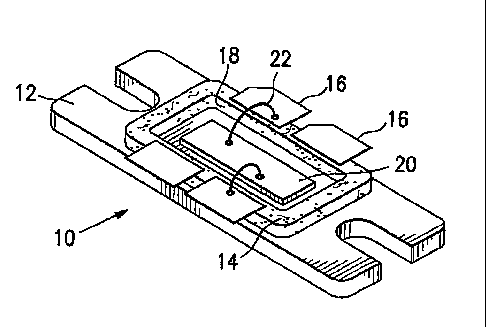
Fig.l shows a semiconductor package 10 in accordance with the
invention. The package 10 of Fig. 1 includes a heat sink flange 12 of
elongated,
flat, generally planar configuration, having a window frame 14 mounted
thereon. A plurality of leads 16 are mounted on the window frame 14 opposite
the flange 12. The window frame 14 has an opening 18 therein exposing a
portion of the flange 12. A semiconductor die 20 is mounted on the flange 12
within the opening 18, and is electrically coupled to the leads 16. Such
electrical coupling may be accomplished with wire bonds 22, two of which are
shown in Fig. 1 for illustration. A single die 20 is shown for purposes of
illustration, and plural dies may be mounted within the opening 18 if desired.
CA 02512845 2005-07-08
WO 2004/064120 PCT/US2004/000621
7
A lid (not shown) may be mounted on the leads l6 so as to extend over and
enclose the opening 18 and the included die 20.
Fig. 2 is an exploded view of several of the components of the
semiconductor package 10 Fig. 1 showing the manner in which they are
assembled to form a header 24. The header 24 includes the flange 12, the
window frame 14 and the lead 1G. The window frame 14 is joined to the flange
12, such as by brazing, following which the leads 16 are mounted in similar
fashion onto the window frame 14 opposite the flange 12. The semiconductor
package 10 is completed by mounting one or more of the dies 20 within the
window frame 14 of the header 24 and electrically coupling the dies 20 to the
leads 16 by wire bonding. Epoxy or other potting compound may then be used
to fill the opening 18, with a lid then being installed over the package 10,
as
desired.
The semiconductor package 10 of Fig. 1 is of conventional configuration,
except for the window frame 14. In accordance with the invention, the window
frame 14, which is shown in enlarged and detailed fashion in Fig. 3, is made
of
non-ceramic based material. Preferably, such material includes a matrix of
principally organic material filled with fibers or other geometrical filler.
The
matrix may comprise PTFE or epoxy. The fibers or filler may consist of glass
or
ceramic.
Unlike the alumina or other ceramic based material typically used for
the window frame in conventional semiconductor packages, the non-ceramic
based material of the window frame 14 according to the invention provides a
number of distinct advantages. The non-ceramic based material of the window
frame 14 provides a close thermal expansion or CTE match to the highly
conductive copper or other materials preferably used for the flange 12. As a
result, when the flange 12, the window frame 14 and the lead 16 are subjected
to high temperature, typically on the order of 400°C or greater, during
brazing
together of such components to form the header 24, the window frame 14
undergoes thermal expansion and contraction at a rate similar to that of the
highly conductive flange 12. As a result, the high thermal stresses present in
prior art structures and methods are avoided (Refer to Table 1 for details).
CA 02512845 2005-07-08
WO 2004/064120 PCT/US2004/000621
8
Moreover, and unlike the ceramic based material of conventional window
frames, the non-ceramic based material of the window frame 14 according to
the invention is not brittle, but rather is flexible in nature, thereby
further
avoiding the fractures and other failures which occur with conventional
structures.
To provide the window frame 14 with a wetable surface for purposes of
brazing or otherwise bonding to the other components, the window frame 14 is
preferably clad with a layer of metal such as copper or aluminum. Due to the
nature of the non-ceramic based material of the window frame 14, it can be
difficult to provide a good bond between the cladding metal and the non-
ceramic
based material. However, a good bond is provided by the technique shown in
Figs. 4A and 4B. Fig. 4A shows the window frame 14 spaced apart from a
cladding layer 24 of metal. A surface 26 of the cladding layer 24 is
roughened,
as shown in Fig. 4A, before the cladding layer 24 is disposed against the
window frame 14. The layer 24 is then laminated to the window frame 14 by
applying pressure and elevated temperature. The non-ceramic based material
of the window frame 14 flows into the roughened surface 26 of the cladding
layer 24. After a sufficient amount of time, the structure is cooled and the
pressure is removed. The final, laminated product is shown in Fig. 4B. As
shown in Fig. 4B, the roughened surface 26 integrates with the window frame
14 to form a very strong bond between materials which are otherwise difficult
to bond together. The cladding layer 24 may then be plated such as with nickel
and gold in preparation for bonding with gold/germanium solder. A preferred
solder has the composition 88Au12Ge, although other solders can be used.
In accordance with a feature of the invention, the cladding and
laminating operation shown in Figs. 4A and 4B can be used to provide the
window frame 14 with a flange attached thereto, at the same time as the
cladding layer is formed. Simply by mal~ing the cladding layer 24 of
sufficient
thickness so as to form a flange of appropriate thickness, such flange is
formed
at the bottom of the window frame 14 as the cladding layer 24 is bonded to the
window frame 14. This eliminates the need to form a separate flange 12 and
attach such flange to the window frame 14.
CA 02512845 2005-07-08
WO 2004/064120 PCT/US2004/000621
9
In accordance with the invention, the flange 12, the window frame 14
and the leads 16 of the header 24 can be joined together using various
processes. As previously noted, gold/germanium solder can be used to join the
window frame 14 to both the flange 12 and the leads 16. Where such method is
used, the window frame 14 is preferably coated with nickel and then gold
following the metal cladding thereof. Alternatively, the window frame 14 can
be bonded without soldering/brazing. This is accomplished using epoxy or any
suitable adhesive. Epoxies have strong adhesion to the non-ceramic based
window frame. At the same time, they are capable of bonding to copper or
aluminum cladding as well as to nickel/gold platting on the window frame 14.
Epoxy can be used to bond the window frame 14 to both the flange 12 and the
lead 16.
As previously described, lamination techniques can be used to join the
flange 12 directly to the non-ceramic based material of the window frame 14.
Also, as previously described in connection with Figs. 4A and 4B, the cladding
layer 24 can be provided with sufficient thickness so that it forms the flange
12
when joined to the window frame 14.
Fig. 5 shows an alternative embodiment of a flange 30 in accordance with
the invention. The flange 30 is like the flange 12 of Figs. 1 and 2 in that it
is of
elongated, relatively thin, generally planar configuration and has a flat
upper
surface 32 thereon. Unlike the flange 12 of Figs. 1 and 2 however, the flange
30
of Fig. 5 has a raised portion or pedestal 34 extending upwardly from a
central
portion of the flat upper surface 32. The pedestal 34 is configured such that
the
outer peripheral thereof fits within the opening 1~ of the window frame 14,
when the window frame 14 is mounted on the flange 30. The pedestal 34 itself
has a flat upper surface 36 defining a die attach area.
Figs. 6A and 6B are sectional views of a portion of a semiconductor
package similar to the package 10 of Fig. 1 but with the flange 30 used
therein.
The flange 30 with its raised pedestal 34 is shown in the lower portion of
Fig.
6B. A portion of the window frame 14 is shown in the upper right hand portion
of Fig. 6B. A lead 16 is bonded on the top of the window frame 14. In the
example of Figs. 6A and 6B, the window frame 14, the lead 16 and the flange 30
CA 02512845 2005-07-08
WO 2004/064120 PCT/US2004/000621
are bonded together by brazing. As can be seen in Fig. 6B, a thin layer 38 of
the brazing material is disposed between the window frame 14 and the lead 16
so as to join such components together. Similarly, a thin layer 40 of the
brazing
material extends along the interface between window frame 14 and the flange
5 30. During bonding of the window frame 14 to the flange 30, the brazing
material of the layer 40 extends along the interface therebetween as shown.
However, the raised pedestal 34 prevents the brazing material from flowing
onto the die attach area formed by the flat upper surface 36 of the pedestal
34.
Dies attached to the header 24 require a relatively smooth surface,
10 typically having a surface roughness of less than 40u. The raised periphery
of
the pedestal 34 of the flange 30 acts as a barrier to prevent flow of the
brazing
material onto the flat upper surface 3G thereof forming the die attach area.
The
pedestal 34 of the flange 30 can be formed by any appropriate technique such
as
by machining or by stamping. Clad material 42 with an optional coating is
shown between the brazing layer 38 and the window frame 14 and also between
brazing layer 40 and the window frame 14.
Again as previously described, lamination techniques can be used to join
the flange directly to the non-ceramic based material of the window frame.
Also, the cladding layer can be provided with sufficient thickness so that it
forms the flange when joined to the window frame. Fig. 7A is a sectional view
of the semiconductor package 10 with the previously described flange 12 which
does not have a pedestal. In Fig. 7B, the window is shown adhered to the
lead 16 and to the flange 12 by cladding. The cladding provides adhesion at
the
interfaces 44 at the opposite surfaces of the window frame 14.
The presently disclosed embodiments are to be considered in all respect
as illustrative and not restrictive, the scope of the invention being
indicated by
the appended claims, rather than the foregoing description, and all changes
which come within the meaning and range of equivalency of the claims are
therefore intended to be embraced herein.