Note : Les descriptions sont présentées dans la langue officielle dans laquelle elles ont été soumises.
CA 02514133 2010-04-16
REVERSE PRINTING
BACKGROUND
Disclosed is a process for forming thin film transistors (TFTs) in
semiconductor devices. More specifically, illustrated herein is a method of
reverse
printing, which involves both deposition and patterning of organic
semiconductor
layers in thin film transistor devices.
Electronic components, including thin film transistors (TFTs) are commonly
formed on silicon-based materials. However, semiconductor devices with organic
active layers and printed electronic components are emerging as an inexpensive
alternative to silicon-based devices. The performance of organic-based devices
may
not match the performance of their silicon-based counterparts in terms of
device
density and reliability under extreme conditions, for example, high or low
temperatures. However, in certain applications, these shortcomings can be
traded
off for economic benefits because organic materials provide the advantage of
producing these devices without the expensive steps associated with silicon
processing. Other advantages of organic-based devices include the greater
mechanical flexibility and easier electronic tunability.
Forming of patterned organic semiconductor layers, which includes deposition
and patterning of organic semiconductor layers, is a significant part of TFT
fabrication. The deposition method has significant effects on the physical
properties
of the resultant semiconductor layer such as the thickness, surface roughness,
film
morphology. These in turn have significant effect on the performance of TFTs.
Patterning of semiconductor layers is also significant, as proper patterning
and
isolating the semiconductor layers into discrete areas may significantly
reduce device
leakage.
Formation of patterned organic semiconductor layers may be achieved by
deposition of semiconductor layers with vacuum deposition, spin coating, dip
coating,
bar coating methods, followed by patterning with conventional
photolithographic
method. Other methods such as vacuum deposition through a shadow and lift-off
patterning, controlling surface energy and spin or dip coating to generate
patterned
organic semiconductor layers have also been reported. However, these methods
are
generally multiple-step processes or complicated. They may not therefore be
1
CA 02514133 2010-04-16
suitable for manufacturing low-cost, large-area devices. An example of the
above-
cited deposition and patterning methods to form a patterned organic
semiconductor
layer is disclosed by H. E. Katz in US Patent 6,403,397. The `397 process
involves
treating a surface to selectively provide regions of greater affinity and
lesser affinity
for an organic semiconductor solution. When the organic semiconductor, or
solution
comprising the semiconductor, is deposited on the treated surface, either the
organic
semiconductor or the organic semiconductor solution de-wets from the lesser
affinity
regions or the resultant film adheres only weakly to the lesser affinity
regions such
that selective removal is readily achieved.
Other references in the field include: C. D. Dimitrakopoulos, et al., US
5,946,551; K. Amundson, et al., US 6,312,971; Suzuki, et al., US 5,079,595.
A method including both deposition and patterning is disclosed by K. E. Paul
in Appl. Phys. Lett. 2003, Vol 83, p2070-2072. Patterned organic semiconductor
layers are formed by directly printing solution of a semiconductor into the
channels
of TFTs via an inkjet printer. However, the method requires a specialized
semiconductor ink that possesses proper viscosity and stability suitable for
printing.
Thus, there is a need for a new process to deposit and pattern organic
semiconductor layers in organic electronic devices.
SUMMARY
Aspects disclosed herein include
a semiconductor device comprising, a surface on a substrate; and a layer of
semiconductor material on the surface, wherein the semiconductor material is
patterned by printing solvents;
a method comprising, providing a surface on a substrate; depositing a
semiconductor layer on the surface; and depositing a pattern of solvent
droplets on
the semiconductor layer via printing to pattern the semiconductor layer on the
surface;
a method comprising, providing a substrate; forming a layer of semiconductor
material on the substrate; and depositing a solvent on the semiconductor layer
to
pattern the semiconductor layer on the substrate;
a method comprising, a) providing a substrate; b) forming gate, source and
drain electrodes; c) forming a gate dielectric layer; d) forming a layer of
semiconductor material in contact with the gate dielectric layer and the
source and
2
CA 02514133 2010-04-16
drain electrodes; e) printing one or more solvents on the semiconductor layer
to
pattern the layer.
According to another aspect of the present invention, there is provided a
reverse inkjet printing method for forming a semiconductor device, comprising:
providing a surface on a substrate;
forming one or more transistor elements on the substrate;
depositing a layer of semiconductor material on the surface of the substrate
and transistor elements;
depositing a pattern of solvent droplets on the semiconductor layer to
substantially dissolve portions of the semiconductor material and form a
patterned
semiconductor layer in accordance with the transistor elements; and
evaporating the solvent, wherein, after the evaporation, portions of the
dissolved semiconductor material resolidifies and redeposits at contact lines
of the
solvent with the semiconductor layer to form sharp patterned semiconductor
features.
According to a further aspect of the present invention, there is provided a
reverse inkjet printing method for forming a semiconductor device, comprising:
providing a substrate;
forming one or more transistor elements on the substrate;
forming a layer of semiconductor material on the substrate;
selectively depositing a solvent on the semiconductor layer to substantially
dissolve portions of the semiconductor material and form a patterned
semiconductor
layer in accordance with the transistor elements; and
evaporating the solvent, wherein, after the evaporation, portions of the
dissolved semiconductor material resolidifies and redeposits at contact lines
of the
solvent with the semiconductor layer to form sharp patterned semiconductor
features.
According to another aspect of the present invention, there is provided a
reverse inkjet printing method for forming a transistor device, comprising:
providing a substrate;
forming gate, source, and drain electrodes;
forming a gate dielectric layer;
forming a layer of semiconductor material in contact with the gate dielectric
layer and the source and drain electrodes;
3
CA 02514133 2010-04-16
selectively depositing one or more solvents on the semiconductor layer to
substantially dissolve portions of the semiconductor material and form a
patterned
semiconductor layer in accordance with the source and drain electrodes; and
evaporating the solvent, wherein, after the evaporation, portions of the
dissolved semiconductor material resolidifies and redeposits at contact lines
of the
solvent with the semiconductor material to form sharp patterned semiconductor
features.
According to another aspect of the present invention, there is provided a
reverse printing method for forming a semiconductor device, comprising
providing a surface on a substrate;
depositing a semiconductor layer on the surface of the substrate; and
depositing a pattern of solvent droplets on the semiconductor layer via
printing to pattern the semiconductor layer in accordance with predetermined
features of the semiconductor device.
According to another aspect of the present invention, there is provided a
reverse printing method for forming a semiconductor device, comprising:
providing a substrate;
forming a layer of semiconductor material on the substrate; and
selectively depositing a solvent on the semiconductor layer to pattern the
semiconductor layer in accordance with predetermined features of the
semiconductor
device.
According to another aspect of the present invention, there is provided a
reverse printing method for forming a transistor device, comprising:
providing a substrate;
forming gate, source and drain electrodes;
forming a gate dielectric layer;
forming a layer of semiconductor material in contact with the gate dielectric
layer and the source and drain electrodes; and
selectively depositing one or more solvents on the semiconductor layer to
pattern the semiconductor layer in accordance with predetermined features of
the
transistor device.
According to another aspect of the present invention, there is provided a
semiconductor device comprising:
a surface on a substrate; and
4
CA 02514133 2010-04-16
a layer of semiconductor material on the surface of the substrate, wherein
the semiconductor material is patterned by selectively depositing one or more
solvents on the semiconductor layer in accordance with predetermined features
of
the semiconductor device.
According to another aspect of the present invention, there is provided a
semiconductor device comprising:
a surface on a substrate;
a gate electrode disposed on the substrate;
a dielectric layer in contact with the substrate and gate electrode;
a source and drain electrode disposed on the dielectric layer;
a layer of semiconductor material in contact with the source and drain
electrodes;
wherein the semiconductor material is patterned by selectively depositing one
or more solvents to substantially dissolve portions of the semiconductor
material on
the semiconductor layer in accordance with the source and drain electrodes,
and,
after the one or more solvents evaporates portions of the dissolved
semiconductor
material resolidifies and redeposits at contact lines of the solvent with the
semiconductor material to form sharp patterned semiconductor features.
BRIEF DESCRIPTION OF DRAWINGS
Figs la-ic is a drawing showing an embodiment of the present invention
employing a two-step reverse printing where an organic semiconductor material
is
first deposited over thin film transistor features without channel
semiconductor on a
substrate, followed by a second step of patterning the semiconductor layer and
where a solvent is used as a printing "ink" agent to form the patterning
corresponding to the desired semiconductor patterns.
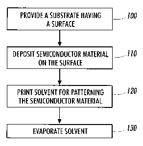
Fig. 2 is a process flow chart showing a two-step method of patterning an
organic semiconductor device employing reverse printing, according to an
embodiment of the present invention.
DETAILED DESCRIPTION
In embodiments there is illustrated methods for depositing and patterning
organic semiconductor layers using a reverse printing method, rather than a
direct
printing process.
5
CA 02514133 2010-04-16
Reverse printing in such methods may provide homogeneity in the film
formed over a semiconductor device, thereby enabling the forming of electronic
components with better performance properties, and may avoid the problems of
printhead blocking that may be encountered in inkjet printing. An aspect of
reverse
printing involves the printing of a solvent at selective locations on a
semiconductor
film for forming the desired semiconductor patterns. At the same time, the
reverse
printing methods may relax otherwise stringent tolerances, thereby making it
more
cost effective than conventional methods in making organic semiconductor
devices.
In one embodiment, the reverse printing method involves patterning a
semiconductor layer by employing a solvent as the "ink" which dissolves a
semiconductor layer already deposited on a substrate to form the desired
patterning
corresponding to the features of a thin film transistor on the substrate. The
method
provides sharper features that improve reliability, and finer lines that
increase the
density of electronic components that can be formed on semiconductor devices.
At
the same time, because the space between transistors is usually larger than
the
channel length of transistors, and that reverse printing can easily
accommodate
lengths of the order of channel lengths, the method can be used to employ
lower
printing resolution and less precise registration to yield cost effective
means for
manufacturing organic semiconductor devices, including active-matrix devices
for
displays such as electronic paper.
In one embodiment, there is a method for spin coating of a solution or
dispersion of the semiconductor materials in a suitable solvent onto a
substrate.
Other deposition methods such as dip coating, solution casting and bar coating
are
also included herein for preparation of the organic semiconductor layer. The
organic
semiconductor layer generally has a thickness from about 5 nanometers to about
1
micrometer, particularly from about 10 nanometers to about 100 nanometers.
The semiconductor in the above method embodiment may first be deposited
on partial or entire surface of the substrate where patterning the
semiconductor
layer into discrete regions is required. After deposition of the semiconductor
layer,
the layer can be optionally dried before printing of solvent to pattern the
layer. The
printing can be performed from about room temperature at 20 C to an elevated
temperature of about 150 C with any suitable printing techniques. Room
temperature printing is preferred. The suitable printing techniques include
screen or
stencil printing, microcontact printing, inkjet printing, and the like.
6
CA 02514133 2010-04-16
Most semiconductor material can be used to form a semiconductor layer. In
one embodiment, the semiconductor is an organic semiconductor, particularly a
soluble organic semiconductor. Exemplary semiconductor materials include
regioregular polythiophenes, oligothiophenes, pentacene precursors, and the
semiconductor polymers disclosed in Beng Ong et al., US Patent Application
Publication No. US 2003/0160230 Al; Beng Ong et al., US Patent Application
Publication No. US 2003/0160234 Al; Beng Ong et al., US Patent Application
Publication No. US 2003/0136958 Al; and "Organic Thin Film Transistors for
Large
Area Electronics" by C. D. Dimitrakopoulos and P. R. L. Malenfant, Adv.
Mater., Vol.
12, No. 2, pp. 99-117 (2002).
The substrate used in the method can be either a "bare" substrate or a
substrate already containing layered material (for example, a conductive layer
and/or
an insulating layer). Accordingly, the surface of the substrate could be a
very
smooth surface or one which has certain features with large surface roughness.
For
example, if a bare substrate is used, the surface roughness can be about
several
angstroms to about 5 nanometers. The substrate of such methods includes
plastic,
glass, or silicon wafer substrate. The organic semiconductor layer may
comprise
polythiophene, oligothiophene, pentacene precursors or thiophene-arylene
copolymer. The solvent droplets may comprise a solvent which is aliphatic
hydrocarbon, aromatic hydrocarbon, alcohol, chlorinated solvent, ketone,
ester,
ether, amide, amine, sulfone, sulfoxide, carboxylic acid, their derivatives,
or mixtures
thereof. The solvent droplets may alternatively comprise a solvent which is
tetrahydrofuran, heptane, octane, cyclohexane, toluene, xylene, mesitylene,
dichloromethane, dichloroethane, chlorobenzene, dichlorobenzene, nitrobenzene,
propanols, butanols, pentanols, dimethylsulfoxide, dimethylformamide,
alkanecarboxylic acids, arenecarboxylic acids, or mixtures thereof. The
dielectric
material may comprise silicon oxide, glass, alumina or plastic, and the gate,
source
and drain electrode materials comprise gold, aluminum, silver, copper, or
PEDOT/PSS.
Illustrative classes of solvents that may be used in the above methods
include, for example, aliphatic hydrocarbons, aromatic hydrocarbons, alcohols,
chlorinated solvents, ketones, esters, ethers, amides, amines, sulfones,
sulfoxides,
carboxylic acids, their derivatives, and mixtures thereof. Illustrative
specific
examples of solvents include for example, tetrahydrofuran, heptane, octane,
7
CA 02514133 2010-04-16
cyclohexane, toluene, xylene, mesitylene, dichioromethane, dichloroethane,
chlorobenzene, dichlorobenzene, nitrobenzene, propanols, butanols, pentanols,
dimethylsulfoxide, dimethylformamide, alkanecarboxylic acids, arenecarboxylic
acids,
and mixtures thereof. If more than one solvents is required, they can be
printed
separately or as a mixture. After printing the solvent onto selective regions
on the
semiconductor layer, the solvent would dissolve the semiconductor layer
locally. The
dissolved semiconductor material would then migrate to the undissolved
semiconductor regions and solidify thereof, thus creating a "void" in the area
where
the solvent is printed.
In fabricating TFTs, it is often desirable to have the semiconductor film
present only at selected regions of a circuit, or selected regions of an
individual
device, to achieve, for example, reduced leakage current and crosstalk. Such
selective formation, or patterning, also enables the use of different
semiconductors
in different regions of a device or in different devices of a circuit.
However, the
organic semiconductor is normally formed as a continuous film covering many
devices when conventional deposition techniques such as spin coating and dip
coating are used. Therefore, subsequent patterning steps are required to form
desired discrete semiconductor layers. It is possible to use established
photoresist
technology to pattern a deposited organic film. However, known methods such as
reactive etching leave unwanted residues and also have the potential danger of
degrading the semiconductor film. As an alternative, for some materials it is
possible
to directly and selectively print, a solution of an organic semiconductor onto
a
substrate such that a semiconductor film is formed upon evaporation of the
solvent.
In contrast to this direct printing, reverse printing involves printing a
solvent onto a
preformed organic semiconductor layer to create "voids" in certain regions on
the
semiconductor layer, resulting in the patterning of the semiconductor layer.
Referring now to the drawings, Figs. 1a-1c disclose a novel method of
forming TFTs using the reverse printing method. The reverse printing is
amenable to
the roll-to-roll manufacturing line, which is a high throughput manufacturing
process.
An embodiment involves the forming of semiconductor materials on a
substrate which may or may not have certain preformed transistor features such
as
electrodes. In Fig. la, two TFTs 10 and 10' are shown for illustrative
purposes.
The TFTs comprising a source electrode 20, a drain electrode 30, and a gate
electrode 60 on a substrate 40. The source and the drain electrodes are
separated
8
CA 02514133 2010-04-16
from the gate electrode by an intervening insulating dielectric material 50 as
shown
in Fig. Ia. Substrate 40 can be conductive, such as silicon, in which case the
substrate can serve as a gate electrode. The substrate can also be an
insulating
material, in which case a gate electrode is formed on the substrate. Suitable
insulating materials include silicon oxide, other oxides such as glass and
alumina,
and polymeric plastic substrates such as polyimide. Typical source, drain and
gate
electrode materials include metals such as gold, silver, copper, chromium,
aluminum,
and conductive polymers such as PEDOT/PSS. Dielectric layer 50 over gate 60
can
be composed of materials including silicon oxide, spin-on glass, and
polyimides.
Materials capable of being handled and applied in a roll-to-roll process are
also used.
The thin film transistors of Fig. Ia, namely 10 and 10', now are covered by a
uniform coating of an organic semiconductor layer 65 shown in Fig. Ib. Layer
65 is
formed by spin coating 15, though any number of other known techniques,
including
dip coating and bar coating, may be used. Following the coating step, the
layer is
optionally dried, to give a homogenous thin layer covering the dielectric
layer 50,
and the source electrode 20 and drain electrode 30 as shown in the same Fig.
Ib.
The organic semiconductor layer 65 in one embodiment is formed by a 1% by
weight solution of a semiconductor polymer such as regioregular poly(3-
hexythiophene) in toluene.
According to one embodiment, a suitable solvent is printed around each
transistor in Fig. lb to pattern the semiconductor layer 65. The step of
printing with
solvent is schematically shown as "ink" droplets 70. In one embodiment of the
present invention, chlorobenzene was used as the solvent to pattern above
semiconductor layer of poly(3-hexythiophene). In another embodiment, the
solvent
of the ink droplet dissolves the semiconductor material around the thin film
transistors 10 and 10'. As a result of the process of reverse printing and
subsequent evaporation of the solvent, the dissolved semiconductor material
resolidifies from the solution and redeposit at the contact line of the
solvent with the
semiconductor material after the evaporative drying takes place. Consequently,
the
solvent printing results in clean and sharp semiconductor features, such as 80
shown
in Fig. Ic.
The two-step process flow of patterning organic semiconductor layers that
may be employed is summarized in Fig. 2. First step 110 involves deposition of
an
organic semiconductor material onto a substrate 100 having certain preformed
TFT
9
CA 02514133 2010-04-16
features followed by a second step 120 of reverse printing a pattern
corresponding
to the features on the substrate. Patterning is complete after evaporation of
the
solvent 130.
Sharper features may improve TFT performance characteristics. On the other
hand, because the space between transistors is usually larger than the channel
length of transistors, and that reverse printing can easily accommodate
lengths of
the order of channel lengths, methods of the present invention may be used
advantageously to employ lower printing resolution and less precise
registration to
yield cost effective means for manufacturing organic semiconductor devices,
including active matrix circuits for displays, such as electronic paper.
Structure and
shape of the semiconductor patterns are not limited only to straight edges,
but
curvilinear, and any other shape used in semiconductor manufacturing are
possible.
The disclosed methods may be employed in other similar process steps that are
too
many to cite. For example, reverse printing can be integrated with other
methods
such as spin or dip coating, vacuum deposition and lift-off patterning to
fabricate
patterned semiconductor devices which are more cost effective for
manufacturing
low cost electronic devices.
It will be appreciated that various of the above-disclosed and other features
and functions, or alternatives thereof, may be desirably combined into many
other
different systems or applications and that alternatives, modifications,
variations or
improvements therein may be subsequently made by those skilled in the art
which
are also intended to be encompassed by the following claims.