Note : Les descriptions sont présentées dans la langue officielle dans laquelle elles ont été soumises.
CA 02514454 2005-07-26
WO 2004/070830 PCT/EP2004/001787
SACRIFICIAL METAL LINER FOR COPPER INTERCONNECTS
Background of Invention
Technical Field
The present invention relates generally to a
semiconductor device and its method of manufacture. More
particularly, the present invention relates to an improved
liner structure, featuring a sacrificial component, especially
for copper metallurgy.
Related Art
The interconnect structure of semiconductor devices
comprises layers (wiring levels) containing conductive wires
separated by interlevel dielectric layers (levels). The
conductive wires are electrically isolated from one another by
the dielectric layers. The conductive wires in each wiring
level are interconnected by conductive vias extending from the
conductive wires in one wiring level, through the interlevel
dielectric layer, to the conductive wires in a second wiring
level. In modern semiconductor devices, the conductiore wires
are partially embedded in or damascened into the dielectric
layers .
As the speed of modern semiconductor devices has
increased, interlevel-wiring capacitance has become a problem.
Methods have been sought to reduce interlevel wiring
capacitance. One solution that is becoming popular is the use
of low-k dielectric materials such as SILKTM (a polyarylene
ether, available from Dow Chemical, Midland, MI), spin on
CA 02514454 2005-07-26
WO 2004/070830 PCT/EP2004/001787
2
glass, polyimide or other polymers. These have replaced
traditional dielectric materials such as silicon oxide and
silicon nitride.
A problem with low-k dielectric materials is that they
are not rigid like the traditional dielectric materials.
Low-k materials are soft, compressible and flexible, have a
low modulus and poor interfacial strength, i.e., they tend to
delaminate or collapse under mechanical and thermal stress
resulting in low yield, poor reliability and higher costs.
Some low-k materials are brittle and tend to crack under
mechanical or thermal stress. Their use in semiconductor
devices presents two problems. First, because the conductive
wires are comprised of metals (such as copper and tungsten),
there is a mismatch in thermal expansion between low-k
dielectrics and the metal which can lead to delamination,
cracking or collapse of the low-k material during manufacture
or in use in the field. Second, since the wires are formed by
a damascene process, which includes a
chemical-mechanical-polish (CMP) step, mechanical stress is
induced into the device during CMP, which can lead to
delamination, cracking or collapse.
Since low-k dielectric materials, damascene wiring
levels, and CMP are basic to the fabrication of high
performance semiconductor devices, a method for reducing or
eliminating stress induced delamination, cracking or collapse
of low-k dielectric layers is highly desirable.
Typically, a barrier or liner structure is deposited in
the via, and a conductive material is deposited in the via on
the liner structure. Prior to disposition of the liner
structure, a cleaning of the via is usually performed,
commonly by sputtering argon into the via. See, e.g., LT. S.
Pat. No. 6,177,347. Because the sputter etching is applied to
sidewalls in the interlevel dielectric, this can lead to
erosion of the dielectric material, which can redeposit on the
CA 02514454 2005-07-26
WO 2004/070830 PCT/EP2004/001787
3
via bottom at the interface with the underlying conductive
wire, resulting in poor reliability.
Thus, there is a need in the industry for an improved
liner structure, particularly for copper metallurical
structures having low-k dielectrics, and an accompanying
method of making such structures
Summary of Invention
It is against this background, that the present invention
introduces a sacrificial component into the liner structure
and its fabrication, which is particularly advantageous for
copper metallurgy with low-k dielectrics. In general, the
improved liner structure includes a combination of liner
layers, where the first liner layer is prozrided prior to via
cleaning. In use, the first liner layer protects the via
sidewalls (usually, low-k dielectric) from erosion during
subsequent processing, such as sputter etching. During such
processing, only first liner material will be removed, rather
than dielectric, and this is not detrimental to interconnect
reliability, robustness or resistance characteristics.
Further, during sputter etching or cleaning, the first liner
layer is removed from the via bottom, to avoid interconnect
contamination during processing and to further enhance
reliability. According to the invention, the via is also
extended into the underlying metalli~ation during etching; and
a second liner layer is provided, which increases surface area
in contact with the underlying metalli~ation. The thicker
liner structure on the via sidewalls adds mechanical strength,
and better adhesion on the via bottom improves reliability,
such as during subsequent thermal cycling. The liner
structure also improves stress migration characteristics,
which are particularly problematic in copper interconnects.
CA 02514454 2005-07-26
WO 2004/070830 PCT/EP2004/001787
4
Tn accordance with the invention, there is provided a method
of forming a liner structure in a via in the fabrication of a
semiconductor device, comprising: providing a metal line over
a semiconductor substrate; providing a dielectric layer over
the metal line; forming in the dielectric layer a via having
sidewalls and a bottom exposing the metal line; depositing a
first liner layer in the via on the sidewalls and the bottom;
anisotropically removing the first liner layer from the
bottom, while leaving the first liner layer on the sidewalls
and while extending the via so that extended portions of the
sidewalls and the bottom penetrate the metal line; and
depositing a second liner layer on the first liner layer left
on the sidewalls and on the extended portions of the sidewalls
and the bottom penetrating the metal line.
Further, in accordance with. the invention, there is
provided a method of forming a metallization structure in the
fabrication of a semiconductor device, comprising: providing a
metal line over a semiconductor substrate; providing a
dielectric layer over the metal line; forming in the
dielectric layer a via having sidewalk and a bottom exposing
the metal line; depositing a first liner layer in the via on
the sidewalls and the bottom; anisotropically removing the
first liner layer from the bottom, while leaving the first
liner layer on the sidewalk and while extending the via so
that extended portions of the sidewalk and the bottom
penetrate the metal line; depositing a second liner layer on
the first liner layer left on the sidewalls and on the
extended portions of the sidewalls and the bottom penetrating
the metal line to form a liner structure in the via; and
depositing a conductor over the liner structure to fill the
via.
Additionally, in accordance with the invention, there
is provided a semiconductor device comprising a liner
structure, comprising: a metal line over a semiconductor
substrate; a dielectric layer over the metal line; the
dielectric layer including a via having sidewalls and a
CA 02514454 2005-07-26
WO 2004/070830 PCT/EP2004/001787
bottom, wherein extended portions of the sidewalls and the
bottom penetrate the metal line; a first liner layer on the
sidewalls but not on the bottom of the via; and a second liner
layer on the first liner layer, the portions of the sidewalls
penetrating the metal line and the bottom of the via.
The foregoing and other features and advantages of the
invention will be apparent from the following more particular
description of embodiments of the invention.
Brief Description of Drawings
The embodiments of this invention will be described in
detail, with reference to the following figures, wherein like
designations denote like elements, and wherein:
Figs. 1A-1E are schematic section views illustrating the
method in accordance with the present invention; and
Figs. 2A and 2B are cross-sectional SEM micrographs of
metalli~ation structures in accordance with the prior art and
the present invention, respectively.
Detailed Description
Referring to the drawings, Fig. 1A shows a semiconductor
structure 1, which comprises a substrate, typically silicon,
Gags or the like, on which devices such as capacitors and
transistors are formed and an insulator thereover. A metal
line 2 is formed over the structure, followed by an insulator
layer 3, which is t~rpically silicon nitride or other suitable
material. ~ne or more additional layers of dielectric 4 are
formed over the insulator layer 3 to provide a dielectric
layer over the metal line 2.
Any suitable dielectric material or materials can be
employed to form the dielectric layer 4, however, it is
preferred that the layer 4 include a low-k dielectric, i.e.
k<3.5, such as spin on glass, porous silicon oxide, polyimide,
CA 02514454 2005-07-26
WO 2004/070830 PCT/EP2004/001787
6
polyimide siloxane, polysilsesquioxane of
p ymer,
benzocyclobutene, parylene N, parylene F, polyolefin,
polynaphthalene, amorphorus teflon, Black Diamond (available
from Applied Materials, Santa Clara, CA), polymer foam or
aerogel, and so forth. In a particularly preferred
embodiment, the low-k dielectric is an oligomer, uncured
polymer or cured polymer comprising the reaction product of
one or more polyfunctional compounds containing two or more
cyclopentadienone groups and at least one polyfunctional
compound containing two or more aromatic acetylene groups
wherein at least one of the polyfunctional compounds contain
three or more groups selected from the group consisting of
acetylene groups and cyclopentadienone groups.
Advantageously, such a material has an ability to fill gaps
and planarize patterned surfaces, while when cured has
relatively high thermal stability and high glass transition
temperature, as well as a low dielectric constant. Additional
details concerning this particular material can be found in
LT.S. Pat. No. 5,965,679, the entire contents of which are
incorporated herein by reference, as well as details
concerning its preparation and use. Other low-k materials
that can be employed will be known to those skilled in the
art, preferably, the metal line 2 comprises copper, although
other metallurgies, such as aluminum, aluminum-copper,
aluminum-copper-silicon, etc., may be used.
Referring to Fig. 1B, a dual damascene opening or via 5
is formed through the dielectric layer 4 and the silicon
nitride layer 3, typically using a conventional two-mask
process. For example, first a trough is formed to a depth.
less than the total thickness of the dielectric layer 4 by
etching regions not covered by a first mask, which is then
removed. Then, a narrower opening is etched in the bottom of
the trough through to the underlying silicon nitride layer 3
using a second mask, which is also removed. Next, the silicon
nitride layer 3 below the narrower opening is removed,
CA 02514454 2005-07-26
WO 2004/070830 PCT/EP2004/001787
7
typically using a CHF3/Oz dry etch. Although the via 5
illustrated in Fig. 1B is a dual damascene feature, it should
be apparent that other features, such as a single damascene
feature, could be formed in accordance with the invention.
Next, as shown in Fig. 1C, a conductive liner is formed
in the via 5. First, a layer 6 comprising a refractory metal
or a compound thereof is deposited, generally conformally, so
as to coat the top surface of the dielectric layer 4 and the
sidewalls 7 and bottom 8 of the via 5. Preferably, the liner
layer 6 is formed from tantalum, tantalum nitride, titanium,
titanium nitride, a titanium-tungsten alloy or a combination
thereof. Advantageously, the liner layer 6 is deposited prior
to any via cleaning, such as by sputtering with argon. In
this manner, the liner layer 6 protects the via sidewalls 7
from erosion, particularly when a low-k material is employed
in the dielectric layer 4. By utilizing a metal film on the
sidewalls 7, erosion protection is achieved, and any knock-off
or re-sputter will removal metal material, which is not
detrimental to interconnect reliability, robustness or
resistance.
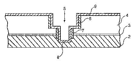
Referring to Fig. 1D, the liner layer 6 is removed from
horizontal surfaces, i.e. from the top surface of the
dielectric layer 4, any horizontal surfaces within the via,
such as formed in a dual damascene feature and the bottom 8 of
the via 5. However, it should be noted that suitable
anisotropic etch conditions are selected so as to leave liner
layer 6 on the via sidewalk 7. In a preferered embodiment,
this can be attained lay carrying out an argon sputter etch.
Importantly, not only is liner layer 6 removed from the via
bottom 5, but additionally there is significant erosion of the
feature into meal line 2. Thus, portions of the via sidewalls
7 and bottom 8 penetrate the metal line 2; in so doing, this
will serve to remove contaminants due to prior processing, and
provide robust interconnect reliability.
CA 02514454 2005-07-26
WO 2004/070830 PCT/EP2004/001787
8
By depositing liner layer 6, prior to any sputter etching
or cleaning, the via sidewalls 7, and thereby dielectric layer
4, are protected from erosion. Performing a sputter cleaning
step on the sidewalls 7, absent any conductive liner, would
likely result in dielectric erosion with re-deposition on the
via bottom 8, leading to poor reliability at the interface
with metal line 2. Additionally, the sidewalls 7 are
protected from re-deposition of metal (e. g. copper), which
could subsequently migrate into the dielectric layer 4,
causing reliability failure or other damage. On the other
hand, by first depositing liner layer 6 on the sidewalls 7,
any re-sputtered metal collects on the surface of the layer 6,
not the dielectric layer 4.
Next, a second liner layer 9 is deposited, generally
conformally, over the dielectric layer 4 and in the via 5, on
the first liner layer 6 left on the via sidewalk 7 and on the
extended portions of the sidewalls 7 and the bottom 8
penetrating the metal line 2, as shown in Fig. 1E. The second
liner layer 9 preferably comprises a refractory metal or a
compound thereof, more preferably, tantalum, tantalum nitride,
titanium, titanium nitride, a titanium-tungsten alloy or a
combination thereof.
Referring to Fig. 1F, after removal of the second liner
layer 9 from the dielectric layer 4, such as by CMP, a
conductive material 10 is deposited, as to fill the via 5, as
well as coating the top surface of the dielectric layer 4.
Then, another CMP process is performed. to remove conductive
material 10 from the top surface of the dielectric layer 4 and
form a coplanar surface of conductive material 10, liner
structure and dielectric layer 4. Any suitable conductive
material 10 may be employed; however, tungsten, aluminum,
aluminum-copper, aluminum-copper-silicon, and copper, are
typical.
CA 02514454 2005-07-26
WO 2004/070830 PCT/EP2004/001787
9
Preferably, the conductive material 10 comprises copper,
where the copper content of the conductive material 10 is
relatively high, generally at least 50%, and preferably above
about 65%, so that the conductive material 10 has a relatively
low resistivity. Tn~h.ile substantially pure copper is generally
preferred, small amounts of other materials may be included
with the copper to, for example, improve resistance to
corrosion. Other materials which may be employed in
accordance with alternate embodiments of the present invention
include, for example, gold, silver, nickel, and so forth.
Preferably, the conductive material 10 is deposited by
electroplating, but other techniques, such as electroless
plating can be employed, as will be apparent to those skilled
in the art. In accordance with the embodiment of Fig. 1F, a
plating base or seed layer is deposited over the second liner
layer 9, using sputter deposition techniques, or other similar
techniques, such as chemical vapor deposition, physical vapor
deposition, etc. In this embodiment, the seed layer is
copper, however, other materials may also be used, such as
tungsten, titanium, tantalum, etc., depending on the form of
plating technique used. Conductive material 10 is then
deposited within the via 5 using an electrolytic plating
technique. In particular, the structure which includes the
via 5 is placed in a container of electroplate solution, an
external current is applied, and the conductive material 10
grows onto the seed layer. Since the seed layer and the
conductive material 10 are both copper in this example, as the
conductive material 10 grows on to the seed layer the division
between the seed layer and the conductive material 10 is
eliminated. Once the via 5 has been filled with conductive
material 10, the surface is planarized using chemical
mechanical polishing or other suitable technique.
It should be noted that by forming the conductive liner
structure in accordance with the invention, a thicker
CA 02514454 2005-07-26
WO 2004/070830 PCT/EP2004/001787
conductive liner results on the via sidewalls 7, providing
enhanced mechanical strength, further improving reliability.
Tn addition, by using a relatively heavy amount of sputtering,
there is significant erosion of the feature into metal line 2,
as noted hereinabove. Preferably, when the metal line 2
comprises copper, the extended portions of the via sidewalls 7
and the via bottom 8 penetrate the metal line 2 by a distance
of at least about 200A, and preferably about 200-1000A. This
results in the conductive liner, as having a greater surface
area in contact with the metal line 2, increasing adhesive
strength of the interconnect, further improving reliability,
such as from thermal cycling during processing.
Without being bound by theory, it is also believed that
improved stress migration results from significant sputter
etch removal in the feature bottom, so as to provide a
recessed feature in the metal line 2 having a stepped
interface. Such improvement in stress migration is
particularly significant as this is a typical failure mode in
a conventional copper interconnect. For example, copper
stress migration results from the movement of vacancies
existing in the copper, and they typically diffuse along grain
boundaries. However, these vacancies can diffuse much faster
along a copper/silicon nitride interface, particularly if
there is poor adhesion between the copper and silicon nitride.
By having a stepped via sidewall/bottom penetrating the copper
line, a blocl~age is created along the copper/silicon nitride
interface, so that vacancies are blocked from moving past this
location. See Figs. 2A and 2B for a comparison of a
metallization structure produced in accordance with the
present invention (Fig. 2B) and. a conventional structure (Fig.
2A) .
While this invention has been described in conjunction
with the specific embodiments outlined above, it is evident
that many alternatives, modifications and variations will be
CA 02514454 2005-07-26
WO 2004/070830 PCT/EP2004/001787
11
apparent to those skilled in the art. For example, the
present invention may be used in conjunction with
semiconductor structures having various features, such as
single damascene, and it is in no way intended to be limited
to use with dual damascene features. It should also be
understood that the conductive liner may comprise, in addition
to the refractory metals or refractory metal compounds
described above, other metals and metal compounds such as WN,
MoN, WSiN, WSi, Nb, NbN, Cr, CrN, TaC, TaSiN, TiSiN, and so
forth. Accordingly, the embodiments of the invention as set
forth above are intended to be illustrative, not limiting.
Various changes may be made without departing from the spirit
and scope of the invention as defined in the following claims.