Note : Les descriptions sont présentées dans la langue officielle dans laquelle elles ont été soumises.
CA 02514869 2005-07-29
WO 2004/068158 PCT/EP2003/001518
Device for sensin a magnetic field
Field of the Invention
The invention relates to a device for sensing a magnetic field.
More specifically, the invention relates to a sensor of magnetic flux using a
superconducting pick-up loop.
Thus the sensor can be used in any magnetic sensor application where the
cooling of the sensor to below the superconducting transition temperature T~
of the
superconducting loop is possible.
Description of the related art
Magnetic sensors are routinely used in many technical applications such as
position, velocity, acceleration, and angle detectors, for example. There is a
large
variety of magnetic sensor types based on different physical principles. The
prior
art relevant to the present invention comprises two kind of sensors:
magnetoresistive (MR) sensors, and sensors based on superconductivity and
SQUIDs (Superconducting Quantum Interference Device). Sensors based on
magnetoresistive elements (MRE) are compact and easy to use with very simple
read-out electronics. The characteristic feature of a SQUID based magnetometer
is
its ultrahigh sensitivity.
The operation of a magnetoresistive element (MRE) is based on the
anisotropic magnetoresistance effect: the resistance of the magnetoresistor
depends on the relative orientation angle between the probing current and the
magnetization vector in the resistor material. A magnetizing field, H, applied
in
the plane of the thin film MRE causes the magnetization vector to rotate, and
a
relative resistance change OR",~/R, typically about 2% is seen over a range of
a
few mT.
Recently MREs based on the so called "giant magnetoresistive effect"
(GMR) have been demonstrated, for example spin valves consisting of two
adjacent magnetic layers. In these GMR devices OR",Q~R-values as large as 15%
have been documented.
The performance of a magnetic sensor is determined by its sensitivity to
the magnetizing field, and the internal noise of the sensor. The sensitivity
of a
GMR element to magnetizing field, defined as S = OR/(R*~Ii), is of the order
of
10~ m/A(corresponding to a resistance change of 0,8% per Oersted). The
intrinsic
noise level of the sensor is defined by converting the apparent resistance
CA 02514869 2005-07-29
WO 2004/068158 PCT/EP2003/001518
2
variations, Rn, due to an internal thermodynamic process into an equivalent
field
noise, B~, using the definition of sensitivity. This leads to B~ _ ~ *H~ _
*R~/(SR), where ~,° is the vacuum permeability.
When measuring a resistor there are two basic mechanisms of
thermodynamic origin resulting in apparent resistance variations: the thermal
voltage noise (white "Johnson noise") and the conductance fluctuations
contributing to the so called 1/f noise dominating at low frequencies.
The spectral density of the white Johnson noise is Un = ~4kTR, where k is
the Bolzmann constant and T the absolute temperature of the resistor. The
field
noise corresponding to this Un is Bn ~,°*(U~/U°)/S, where
U° is the bias voltage of
the MRE resistor. Assuming R=600 Ohms, T=300 K, and Uo 1 Volt we get
Bn 4* 10-Il T/~Hz. This gives the resolution in the white noise range of a
magnetic
sensor based on GMR.
The spectral density of the conductance fluctuations responsible for the
intrinsic 1/f noise, is described by the Hooge relation ~R/R = (~yH/N/f)1/2.
Here N is
a number proportional to the volume of the resistor. In several studies on the
1/f
noise (F. N. Hooge in IEEE Transactions on Electron Devices, vol. 41, no. 11,
1994, and references therein) it has been shown that by .identifying N with
the
total number of current carriers (conduction electrons) in the resistor a
"Hooge
constant ", yH, can be defined, which is universal in the sense that it equals
to 10~
to 10-3 for most resistance materials relatively free of defects and
impurities. For
GMR elements Hooge constants of 6* 10-3 have been measured at room
temperature (based on an assumption of a free electron density of 1/(2*10-
'°m)3).
With these numbers a 1/f field-noise of Bn ~ *(~yH/N/f)I~Z/S=5*10-
1°T/f"Z is obtained
for a typical size GMR element having length of 120 ~,m, width of 6 ~,m, and
thickness of 50 nm.
By far the most sensitive magnetic sensors available at present are those
based on superconductivity and SQUIDS. These sensors utilize two phenomena
associated with superconductivity: the Josephson effect, and the Meissner
effect.
The Josephson effect is a quantum mechanical interference effect
characteristic to an electron system in the superconducting state . This state
is
achieved when the superconducting material is cooled to below its
superconducting transition temperature T~. For classical superconductors T~
is. less
than 10 K. This cooling requirement, of course, limits the technical
applicability
of these magnetic sensors. The limitation is much less stringent if the
recently
CA 02514869 2005-07-29
WO 2004/068158 PCT/EP2003/001518
3
discovered high-T~ superconductors can be used. For these materials T~ is
higher
than SOK, which is achievable by relatively simple cooling techniques.
The technical device utilizing the Josephson effect in measuring weak
magnetic fields is called Superconducting Quantum Interference Device (SQUID).
The apparent resistance of the SQUID depends periodically on the magnetic flux
~SQ B*ASQ flowing through the SQUID loop of area ASQ. As compared to MREs,
this dependence of resistance on the flux is very steep because the period of
the
resistance variation is extremely .small, equal to a constant of nature called
"flux
quantum", ~o = 2*10-'S Wb. Typically, for any SQUID OR/O~S~/R = DU/O~SQIU
is equal to a few times 1/~0. It is this steep dependence of the resistance on
the
magnetic flux that is responsible for the superior sensitivity of the SQUID-
based
magnetic sensors.
The sensitivity of a SQUID to be compared with that of an MRE is
S=OR/R/~H=~.o*~U/LTIOB=~ *(DU/0~5~/U)*ASQ. Optimal internal noise
properties are obtained with a SQUID loop having a rather low inductance, LSQ,
of
the order of 10 pH, which requires a surface area ASQ as small as 10* 10 ~,m2.
Even
for such a small SQUID the sensitivity is 0,1 m/A, which is by a factor 1000
better
than the sensitivity of a GMR device.
Even this high sensitivity of the "bare" SQUID is not sufficient for the
. most demanding applications like biomagnetism, for example. Therefore, a
flux
transformer technique based on the Meissner effect is applied. The idea in
this
technique is to magnify the magnetic flux through the SQUID by effectively
increasing the surface area of the sensor beyond the small ASQ of the bare
SQUID
loop.
The flux transformer is simply a closed superconducting loop. As a
manifestation of the Meissner effect a persistent current arises in such a
loop when
an effort is made to alter the magnetic flux flowing through the loop by any
external source of magnetic field in the vicinity. This persistent current
running in
the loop does not decay with time but stays at the level needed to exactly
compensate for the flux due to the external cause. In the flux transformer
technique this current that is proportional to the momentary external magnetic
flux
through the relatively large flux transformer loop is inductively coupled to
the
SQUID-loop as effectively as possible.
The maximal flux transfer coefficient that can be obtained with the flux
transformer technique is T = ~SQ/~f~ _ (LSQ/2L~)'~2, where ~SQ and LSQ, and
~f~ and
Lf~ are the magnetic fluxes and inductances of the SQUID loop and the flux
CA 02514869 2005-07-29
WO 2004/068158 PCT/EP2003/001518
4
transformer loop, respectively. The best achievable SQUID sensitivity when
using
a flux transformer is the sensitivity of the bare SQUID multiplied by
T*Af~ASQ,
where Aft is the area of the large pick-up coil of the flux transformer.
As mentioned above, to optimize the internal flux noise properties of the
SQUID a low LSQ = 10 pH is preferred. On the other hand, to maximize the flux
~~, and thus the signal of the sensor a pick-up coil area A~ as large as
possible is
chosen. In the biomagnetic applications, for example, where the samples are
large
and extreme sensitivity is necessary, the diameter. of the pick-up loop may be
a
couple of centimeters, so that A~= 4 cmz. Typically, this results in L~ 200
nH,
which means a rather large inductance mismatch between the flux transformer
and
the SQUID, thus limiting the maximal achievable flux transfer coefficient to
.as
low as 7*10-3. In this example the total enhancement by factor T*A~/ASQ 25000
over the sensitivity of the "bare" SQUID is obtained. This results in S = 200
m/A, a sensitivity by factor 3*10' larger than that achievable with a GMR.
A modern low-Tc SQUID with LSQ =lOpH has an intrinsic flux noise
density of ~n = 10-6*~~/~Hz. This limits the intrinsic field resolution of a
SQU>D
based magnetometer utilizing a superconducting flux transformer with a 4 cm2
pick-up coil area to B~ _ ~n/T/Af~ = 10'5 T/~Hz. In practical devices made for
biomagnetic applications this resolution, obtained ~by assuming ideal
inductive
coupling, is not quite reached. A typical technically feasible number is
rather 2 to
3 * 10-'5 T/~Hz. This resolution is by factor 2* 105 better than the
resolution
achieved with a conventional GMR sensor.
The 1/f noise spectral density of a SQUID+flux transformer-based
magnetic sensor determined by the 1/f flux noise intrinsic to a 10 pH SQUID
itself
is of the order of 2 fT/f"2 if ideal inductive coupling is assumed and about 4
f'T/f"2,
assuming a technically feasible coupling.
The SQU)D-based sensors of the prior art utilizing low temperature
superconductors, like niobium, have an excellent noise performance, but the
cryogenics technology required for cooling the sensors to the working
temperature
below T~ is expensive and may even be impossible to implement in some
applications. Relatively heavy dewars are a prerequisite of liquid helium
based
cryogenics. Cooling a geomagnetic flux-gate to liquid helium temperature every
time the device is used in the field is not practical.
Consequently, a lighter technology based on high-Tc superconductors and
liquid nitrogen as the cooling agent has been considered as a promising step
forward in the field of ultrasensitive magnetic sensors. Biomagnetic sensors
based
CA 02514869 2005-07-29
WO 2004/068158 PCT/EP2003/001518
on high-Tc SQUIDS with internal white noise performance in the range of 10
fT~Hz have been reported (ref. : Robin Cantor, Luke ~ P. Lee, Mark Teepe,
Vladimir Vinetskiy, and Joseph Longo, "Low Noise Single-Layer YBaCuO DC
SQUID Magnetometers at 77 K, IEEE Transactions on Applied
5 Superconductivity, vol 5, no. 2 June, 1995, pages 2927-2930).
The problems with the high-Tc SQUID technology are associated with the
low yield, lack of chemical stability, and high price of the high-T~ SQUIDs.
Efficient mass production of high-T~ SQUIDs is difficult because of the
techniques used in making the weak links necessary for the quantum
interference
phenomenon. Whereas the weak links in the niobium SQUIDs are simply realized
by a thin insulator layer between two niobium layers on top of each other
similar
multilayer structures of high-T~ material have turned out to be difficult to
make.
The lack of multilayer high- T~ technology also prevents the fabrication of
efficient multi-turn fluxtransformers .
Because of these technical limitations associated with the mass production
of high-Tc SQUIDs, "hybrid" magnetic sensors based on combination of pick-up
antennae made of a single layer high- T~ film, and "bare" magnetic sensors,
Hall
sensors and GMRs, have been proposed in the prior art (Kaiser et al.,
Cryogenics
38, (1998), patents DE 19944586 C1, DE10041797).
The Cryogenics article introduces an idea of a high-T~ superconducting
pick-up loop coupled inductively to a Hall sensor fabricated by lithographic
technique on the same substrate adjacent to the loop. To enhance the inductive
coupling the pick-up loop is equipped with a narrow "incoupling line" next to
the
Hall sensor, and the superconducting contact leads of the Hall sensor are used
to
further guide the flux through the Hall element. By this construction a field
gain
by factor 100 is obtained for a 4*4 mmz pick-up loop. A sensitivity better
than 20
pT/~Hz above 100 Hz and better than 10 pT~Hz above 500 Hz is reported.
In the patent DE 19944586 C1 a reference is made to the Cryogenics
article and the idea is further developed. The main claim defines a
symmetrized
gradiometer device utilizing a double loop pick-up coil and a Hall element
synunetrically divided on both sides of the incoupling line. An idea of using
the
pick-up loop as one of the Hall electrodes is also introduced. The use of MRE
or
GMR is presented in a subclairn referring to the main claim on symmetrized
device provided with a divided sensing element. The patent DE 10041797 refers
to the preceding one and claims further refinement of the pick-up coil
arrangement
aiming at balancing the sensor against uniform magnetic field.
CA 02514869 2005-07-29
WO 2004/068158 PCT/EP2003/001518
6
In all this prior art the magnetic sensor elements are located adjacent to the
incoupling line, or in the gaps between the multiple antenna loops. This is
the
natural geometry enabling the use of Hall sensors: the amplified magnetic
field is
orthogonal to the plane of the Hall sensor.
Summary of the invention
The present invention aims at overcoming the above-mentioned drawbacks
and in particular at avoiding the use of Hall sensors or SQUIDs whilst
allowing
the production of a sensing device having comparable or better performances
than
the known magnetometers.
The invention further aims at providing a compact and reliable sensor.of
magnetic flux which is easy to produce and may be used in any magnetic sensor
application including biomagnetic detection.
The invention further aims at improving the sensitivity of the sensing
devices for sensing a magnetic field in different applications.
These aims are achieved due to a device for sensing a magnetic field,
wherein it comprises a closed superconducting pick-up loop having a path width
d etched out of a single layer superconducting. thin film of thickness el, and
provided with a constriction having a width w of narrow dimension smaller than
said path width d, said closed superconducting pick-up loop constituting a
flux-to-
field transformer (FFI~T), and wherein at least one magnetoresistive element
is
placed on top of or below said superconducting thin film, is isolated from
said
superconducting thin film by a thin insulating layer of thickness e4 smaller
than
said width w, and is located so that an active part of the magnetoresistive
element
is at the location of the constriction and has a width W~,,,~ equal to or less
than the
width w of the constriction, the active part of the inagnetoresistive element
being
oriented so that the bias current in said active part is directed essentially
along the
constriction, orthogonally to the width w of narrow dimension.
Preferably, the magnetoresistive element is based on the giant
magnetoresistive effect and constitutes a GMR resistor.
It may also consist of Tunneling Magnetoresistive (TMR) element or
Colossal Magnetoresistive (CMR) element.
Advantageously, the superconducting pick-up loop is made of high-T
superconductor having a superconducting transition temperature T~ higher than
50 K.
CA 02514869 2005-07-29
WO 2004/068158 PCT/EP2003/001518
7
Thus cooling of the sensor to below 9 K is required if the loop is made of a
material which is a low-Tc superconductor such as niobium, whereas cooling is
required only to below values such as 50 to 90 K, e.g. ~0 K if the pick-up
loop is
made of high-T~ superconductors.
The magnetoresistive element has a thickness (e2) of a few tens of
nanometers.
According to a specific embodiment of the invention, the constriction of
the pick-up loop is wounded in a coil, whose self induction is of the same
order of
magnitude (ideally equal) than the self induction of the rest of the pick-up
loop
constituting the receiving loop, said coil being wound around a core
comprising a
magnetoresistive bar constituting the field sensox.
Preferably, the constriction has a reduced width comprised between a few
tenths of micrometer and a few micrometers.
According to a preferred embodiment, the circumferential path of the
superconducting pick-up loop defines a circumferential path which is
essentially a
convex loop, like a square or a circle having a mean diameter D.
According to an advantageous embodiment, the superconducting pick-up
loop is essentially a symmetrical double loop having a eight shape and the
constriction of the superconducting pick-up loop is located on the central
common
branch of the eight-shaped loop, defining two elementary flux-to-field
transformers (FFDT).
Advantageously, the additional coil inductively coupled to the pick-up
loop is a plane type coil only coupled to one of the elementary flux-to-field
transformers.
According to a specific embodiment, the device according to the invention
further comprises a negative feed-back loop having a feed-back current driven
into
an additional coil inductively coupled to the pick-up loop to counteract an
external
magnetic flux and to thus prevent the appearance of a Meissner current in the
pick-up loop.
According to still another specific embodiment, the device according to the
invention further comprises means for providing a negative feedback, said
means
comprising a normal metal bridge placed on top of the magnetoresistive element
and means for driving a current through said normal metal bridge to create a
flux
density used to cancel the flux density caused by an induced Meissner current.
The mean diameter (D) of the circumferential path of the superconducting
pick-up loop is comprised between a few millimeters and a few centimeters.
CA 02514869 2005-07-29
WO 2004/068158 PCT/EP2003/001518
g
More specifically, the mean diameter (D) of the circumferential path of the
superconducting pick-up loop is comprised between about 1 and 3 centimeters
and
the device is applied to biomagnetic detection.
The invention thus concerns an optimal way of combining a thin film
superconductor loop with a magnetoresistive sensor into a hybrid sensor having
a
performance comparable to state of the art SQUID based magnetometers.
The hybrid sensor consists of a pick-up-loop patterned from a
superconducting thin film and provided with a narrow incoupling line. The
innovation of the present invention is based on the fact that whereas the
signal of a
SQUID or a Hall sensor is proportional to the total flux through these sensors
the
signal of a magnetoresistive element such as a GMR element is proportional to
the
magnetic flux density in the plane of the sensor. Thus, contrary to the case
of
SQUID and Hall sensor a large total flux is not needed because the GMR sensors
are very thin, typically 50 nanometers thick. It is sufficient to place such a
sensor
at the "hot spot" where the flux density is at its maximum. When the GMR
sensor
having the same width as the incoupling line is placed directly on top of the
incoupling line a high field gain efficiently controlled by choosing the width
of
the incoupling line is obtained. In this way one gets out of a single layer of
thin
film High-Tc superconductor a very efficient "flux-to-field transformer"
(FFDT).
No flux guiding structures such as the superconducting electrode planes
characteristic to the prior art Hall devices are needed.
Because of the efficient inductive coupling geometry the field gain,
obtained by a given incoupling line width, exceeds that of a superconducting
loop
+ Hall sensor hybrid by a factor of ten. This results in a sensor performance
comparable with the state of the art low- T~ SQUID based sensors if
magnetoresistive elements having a sensitivity of 6*10~4 (5%/Oe) are
available.
In the present invention a superconducting loop etched out of a single layer
thin film is used as a FFDT that transforms the magnetic flux flowing through
the
pick-up loop into a high local field B~,~ at a singular point on the
circumference
of the loop. The tiny GMR element is then placed at this "hot spot".
Contrary to the case of the flux transformers used in the SQUID-based
devices of prior art where only less than 1 % of the total flux of the flux
transformer is transmitted through the SQUID loop, the FFDT is able to enhance
the magnetic field locally at the site of the GMR element roughly by a factor
of
BG~Bo (~ to ~t12)*(D/w~~), where D is the mean diameter of the
CA 02514869 2005-07-29
WO 2004/068158 PCT/EP2003/001518
9
superconducting loop and w~,,,m is the common width of the narrow incoupling
line
and of the GMR element sitting on top of this constriction.
For the large FFDT-loops where D = 2 to 3 cm that can be used in the
biomagnetic application the field enhancement B~~Bo can be of the order of
10000, if for example w~~ 4 ~.m. This results in a corresponding enhancement
in
the sensitivity as compared to using a "bare" GMR. If, in addition to the
field
gain, the reduction in the thermal voltage noise - resulting from the cooling
of the
GMR from 300 to g0 K - is taken into account, a resolution of the GMR in the
white noise regime is improved to Bn=5*10-'S T/~Hz, which would be sufficient
even for the biomagnetic application.
It is possible to reduce the l/f noise, by a modulation of the AC current
and by choosing a working point for the GMR where the second derivative of
R(H) is maximal. In that case, low frequency fluctuations are measured around
the
second harmonics of the AC frequency. The improvement is the suppression of
the 1/f noise with a decrease of the sensitivity by a factor about 4.
In the flux gate applications where larger field variations must be dealt
with and the extreme fT-level sensitivity is not necessary a smaller size FFDT
with a wider constriction can be used. In this way the working range of the
sensor
can be moved toward higher fields. The dynamic range will stay the same
because
an FFDT with smaller loop and wider constriction tolerates a higher flux
without
exceeding the critical current of the constriction.
The sensitivity of 1 pTl~Hz, can still be achieved with devices as small as
10 ~.m about in diameter. This exceeds the sensitivity of the prior art flux-
gates by
a factor of more than ten. The frequency range covered by the sensor ranges
from
DC to an upper limit determined by the speed of the reading electronics.
The dynamic range may be further modified by using negative feedback.
In this technique a flux density associated with a current driven through a
normal
metal bridge on top of the GMR element is used to cancel the flux density
caused
by the induced Meissner current. In this case the dynamic range and
sensitivity of
the device is determined by those of the current source used for feedback.
Brief description of the drawing-s
These and other objects and features of the present invention will become
clearer from the following description of specific embodiments given by way of
example with reference to the accompanying drawings, in which:
CA 02514869 2005-07-29
WO 2004/068158 PCT/EP2003/001518
- Figure 1 is a schematic view of an example of a sensor according to the
invention with a square shaped superconducting flux guide loop provided with a
narrow constriction,
- Figure 2 is an enlarged view of a portion of the sensor of Figure 1
5 showing a close-up of the constriction with a GMR element on top of it,
- Figure 3 is a cut view along line III-III of Figure 2 showing at the level
of
the constriction the GMR element on top of the superconductor separated from
it
by an insulator thin film
- Figure 4 is a cut view similar to the cut view of Figure 3 at the level of a
10 constriction corresponding to a variant embodiment where a negative
feedback
technique is used.
- Figure 5 is a schematic view of another example of sensor according to
the invention with a superconducting flux guide consisting of two symmetric
loops, and
- Figure 6 is a schematic view of another example of sensor according to
the invention with a superconducting constriction extended and wired around a
magnetoresistive element.
Detailed description of preferred embodiments
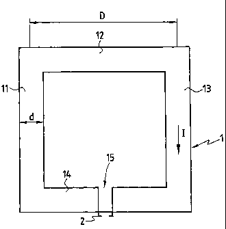
The physical working principle and basic design of a magnetic sensor
based on the present invention is shown in Fig. 1. The superconducting flux
guide
1 consists of a square shaped closed loop lithographically etched out of, for
example, a high-Tc superconductor thin film. The loop comprises a
circumferential path with a first branch 12, two lateral branches 11, 13 and a
fourth branch 14 which is parallel to the first branch 12.
A change ~B in the magnetic field component perpendicular to the plane
of the loop 1 induces a change DI in the persistent current I circulating in
the loop
1. The magnitude of DI is determined by the requirement that the total flux
through the closed superconducting loop stays constant (Meissner effect).
Therefore, 0I = OB*A~.,IL~T, where ACT and LET are the surface area and
inductance of the loop 1.
The inductance of a square shaped loop of superconducting thin film is
LET = (~,~/2~)*D*[Ln(4D/d)-2.35] (see Fig. 1). To simplify the formulas below
we choose d=0.14*D, whence LET = (~,~/2rt)*D.
D which is called the mean diameter of the loop represents in this example
the distance between two parallel branches 11, 13 of the circumferential path
of
CA 02514869 2005-07-29
WO 2004/068158 PCT/EP2003/001518
11
the square-shaped superconducting pick-up loop 1. D may be comprised between
a few millimeters and a few centimeters.
The width d of the branches 11, 12, 13, 14 of the circumferential path of
the pick-up loop 1 is related to D and as explained above may be for example
chosen as d = 0.14*D.
The circumferential path of the pick-up loop 1 has a small thickness e,, e.g.
a few tens of nanometers.
The pick-up loop 1 constitutes a flux-to-field transformer (FFDT) loop
having a portion 15 that transforms the magnetic flux flowing through the pick-
up
loop 1 into a high local magnetic field at a singular point on the
circumferential
path of the superconducting pick-up loop 1.
At least one magnetoresistive element 2 such as a GMR element is placed
on top of the singular point constituting a narrow constriction 15 having a
width
w«d (Figures 1 to 3) and the magnetoresistive element 2 is isolated by a thin
insulating layer 4 of thickness e4 which is smaller than the width w and also
preferably smaller than the thickness e, of the superconducting film 1 and/or
the
thickness e2 of the magnetoresistive element 2.
The narrow constriction 15 having a strongly reduced width w compared
to the defined path width d is formed in the complete thickness e, of the
circumferential path of the loop 1 and the magnetoresistive element 2 is
located on
the top of the constriction 15 of the reduced width.
The magnetoresistive element 2 is located so that the active part of the
magnetoresistive element 2 is at the location of the constriction 15 and has a
width
W~",~ equal to or less than the width w of the constriction 15. The active
part of
the magnetoresistive element 2 is oriented so that the bias current in the
active part
is directed essentially along the constriction 15, orthogonal to the width w
of
narrow dimension.
The narrow constriction 15 can be located at any technically convenient
location on the circumference of the FFDT -loop. Usually, the loop has a
rectangular shape and the narrow constriction is located towards the middle of
one
of the great sides.
The yoke-type shape embodiment of the GMR-element 2 is a standard
design used in MREs to stabilize the magnetization pattern. The active area of
the
element, having a resistance R, is the middle section between the biasing
electrodes 3. This area is chosen some distance away from the corners to make
CA 02514869 2005-07-29
WO 2004/068158 PCT/EP2003/001518
12
sure it is free of magnetic domain walls. This is to avoid extra resistance
fluctuations arising from moving magnetic walls.
The positioning of the GMR element 2 on top of the constriction 15 may
be done mechanically, if it is on a different substrate or, preferably, it may
be
patterned by using lithographic technique directly on top of the constriction
15.
The latter method guarantees an optimal tight coupling to the FFDT-loop.
Alternatively, the magnetoresistive element 2 may be placed below the
superconducting thin film 1.
The GMR element 2 contains high permeability material, with ~,t 8000,
typically. Deposition of even a small amount of such material on top of the
FFDT
-loop will increase the inductance of the loop by an amount L~~, and result in
a
decrease of the induced DI. L~~ is proportional to the volume of the GMR
element, which should therefore be kept reasonably small. On the other hand
the
amplitude of the 1/f voltage noise associated with the conductance
fluctuations is
proportional to the inverse square root of the volume of the active area of
the
GMR resistor. The optimal signal to noise ratio at low frequencies is thus
obtained
with a GMR so large that L~~ = LET, so that the current change induced by the
change in field, OB, is reduced to DI = 0B*A~.ll(2*L~T).
By Ampere's law the circulation of the magnetic field around a closed path
is equal to ~,o times the total current through the loop of the path. When
this is
applied to the closed path 3 in Figure .3, having a total length of
approximately
2*w~,~, the change in the magnetic field at the location of the GMR element 2,
as
a response to 0B through the loop, is approximately
~c~ ~0~~(2~~'~'c~)=~-~o~Ar-w~('~~'L~T~wc~)*~=(~2)~(D/w~~)~~~
when a square shaped FFDT-loop is assumed (ACT D2).
The resulting field gain factor (~c/2)*(D/w~MR) for a given size of FFDT
loop is controlled by choosing the width w~,~,R. For a large loop with D= 2 cm
applicable in biomagnetic detection the gain factor can be as large as 10000.
This
is an important advantage of the present invention.
The magnetoresistive element 2 may have a thickness e2 of a few tens of
nanometers.
The dynamic range may be further modified by using negative feedback.
As shown in Figure 4, the flux density associated with a current driven
through a
normal metal bridge 6 on top of the GMR element 2 is used to cancel the flux
CA 02514869 2005-07-29
WO 2004/068158 PCT/EP2003/001518
13
density caused by the induced Meissner current. An insulating layer 5 is
deposited
in between to avoid electrical contact. In this case the dynamic range and
sensitivity of the device is determined by those of the current source used
for
feedback.
One may also provide the device with negative feed-back by a feed-back
current driven into an additional coil equivalent to bridge 6 and inductively
coupled to the FFDT-loop to counteract the external magnetic flux and to thus
prevent the appearance of the Meissner current in the FFDT-loop.
A variant of an FFDT geometry intended for measurement of the gradients
of the magnetic field is a symmetrical double loop having a eight shape whose
each of the two elementary loops is a' square, and the constriction settles in
the
portion of conductor common to those two elementary loops, as shown in Figure
5. This kind of a sensor results in a better signal to noise ratio in
conditions where
signals from sources at a short distance are to be resolved from large
background
fields arising from sources far away.
The superconducting flux guide 101 of Figure 5 consists of two elementary
symmetric loops. In this geometry, the current running through the
constriction
115 in the center branch 114 is proportional to the gradient aB~/ay of the
magnetic
field.
Thus in the embodiment of Figure 5, the superconducting pick-up loop 101
is essentially a symmetrical double loop having a eight shape and the portion
1.15
at a singular point of the pick-up loop 101 is located on the central common
branch 114 of the eight-shaped pick-up loop 101.
On Figure 5, the "upper" loop comprises an upper branch 112a, two
parallel lateral branches llla,113a which may define a distance D or "mean
diameter" as on Figure 1 and the common branch 114 which is parallel to the
upper branch 112a.
The "lower" loop comprises a lower branch 112b, two parallel lateral
branches 117b, 113b which are extensions of branches llla, 113a and the
common branch 114 which is parallel to the lower branch 112b.
The path width d of branchesllla, lllb, 112a, 112b, 113a, 113b, 114 is
defined as a function of D as explained with reference to Figure 1 in
connection
with loop 1.
The width w of the constriction 115 is much smaller than the path width d
as also previously explained with reference to Figure 1 in connection with
constriction 15.
CA 02514869 2005-07-29
WO 2004/068158 PCT/EP2003/001518
14
The features of the magnetoresistive element 2 located on top of the
constriction 115 are similar to the features of the magnetoresistive element 2
of
Figure 1 and will not be repeated. The explanations given with reference to
Figures 2 to 4 thus apply also to the embodiment of Figure 5.
However, as shown on Figure 5, the constriction 115 is designed in such a
manner that the pick-up loop 101 is symmetrical. The constriction 115 is thus
arranged at mid-height of the path width d in the common branch 114. Moreover,
the portions 114, 117 of the common branch 114 contiguous to the constriction
115 preferably have a V-shape.
Thus the sensor according to the invention may sense a very small
magnetic field with a magnetoresistive element 2 located at' the level of the
constriction 115 which is common to the loops of the eight-shaped loop 101
without any need for delocalizing such transducer.
In case of need, two or more magnetoresistive elements 2 may be located
along the constriction 15 (Figure 1) or 115 (Figure 5) whose length should be
adapted accordingly.
One may combine the FFDT geometry intended for measurement of the
gradients of the magnetic field, as shown on Figure 5, with the above negative
feed-back device using an additional coil inductively coupled to the FFDT pick-
up
loop. In this case, the additional coil must be not symmetrically coupled to
the two
elementary loops of the gradient sensor. In a preferred embodiment, this
additional
coil is a plane type one, positioned in a plane parallel to FFDT plane, and
only
coupled to one of the FFDT elementary loops. For instance, it is a single turn
coil
covering one fourth of one of the elementary FFDT loops. The negative feedback
loop having a feed back current driven into the additional coil inductively
coupled
to the pick-up loop as mentioned above counteracts the external magnetic flux
and
thus prevents the appearance of a Meissner current in the FFDT pick-up loop.
Figure 6 relates to another embodiment of the present invention and shows
how the constriction 215 can be elongated to a wire 211 and wounded around a
magnetoresistive element 212 constituting a bar, either with lithography
techniques or mechanically. The coil 211 may be made of a wire having a
smaller
diameter than the main coil (not shown) cooperating with the superconducting
pick-up loop 201 to allow a higher number of turns. In lithography techniques,
the
number of turns is limited. The number of turns has also to be limited so that
the
inductance of the wound constriction 211 does not exceed too much the
inductance of the rest of the main loop 201.
CA 02514869 2005-07-29
WO 2004/068158 PCT/EP2003/001518
Figure 6 shows a superconducting pick-up loop 201 comprising a
circumferential path which essentially defines a ring or circle having a mean
diameter D and a path width d which is substantially greater than the diameter
of
the wire 211 of the coil defining the constriction 215.
5