Note : Les descriptions sont présentées dans la langue officielle dans laquelle elles ont été soumises.
CA 02518613 2005-09-09
WO 03/092119 PCT/IB03/02272
1 P/63086.WOP5
ANTENNA FOR A WIRELESS LOCATION DEVICE AND METHOD
This application relates to wireless communication device. Such devices are
described in our U.S.Patents Nos. 6,483,473 and 6,501,435, the disclosures of
which are
hereby incorporated by reference in their entireties.
The present invention relates to an apparatus, system and methods of providing
a
wireless communication device and communicating information concerning an item
containing the wireless communication device.
It is often desired to track and identify items, such as packages, containers,
etc., and to communicate information concerning such items wirelessly. One
method of
tracking and providing information concerning packages is to attach a wireless
1o communication device, such as a radio frequency identification (RFID)
transponder or
other identification device, to packages. The information communicated
concerning the
packages may include expiration dates, "born on" dates, lot numbers,
manufacturing
information, and the like. A wireless communication device may be attached to
an
individual package or to a container containing multiple packages.
15 A problem exists when a wireless communication device is attached to
packaging or containers constructed out of a conductive material such as foil.
A pole
antenna connected to the wireless communication device will not radiate
properly if the
wireless communication device is attached on the outside of the package. The
pole
antenna will be shielded if the wireless communication device is placed inside
the
2o package.
It may be advantageous for such a wireless communication device to
communicate on different frequencies so that one device can be used for
various
CA 02518613 2005-09-09
WO 03/092119 PCT/IB03/02272
2 P/63086.WOP5
applications. For instance, an operating frequency of 2.45 GHz is used
frequently
outside the United States, but an operating frequency of 915 MHz is frequently
used in
the United States. Many companies manufacture wireless communication devices
that
are capable of operating at both 915 MHz and 2.45 GHz frequencies so that
either
frequency can be chosen for operation. However, wireless communications device
applications, such as attaching wireless communication devices to packages for
informative and tracking purposes, configure the device to communicate on only
one
frequency -- either a frequency for the United States or a frequency for use
abroad. It
would be advantageous to construct a wireless communication device with an
antenna
1o structure that is capable of communicating at more than one frequency. This
would
allow one wireless communication device to be applicable for uses in both the
United
States and abroad.
In addition to conductive materials, wireless communication devices are also
used with many other substrates. Each substrate has its own dielectric
characteristics,
15 which typically affect the impedance matching between the wireless
communication
device and its antenna. Impedance matching ensures the most efficient energy
transfer
between an antenna and the wireless communication device.
Further, there are occasions when it may be desirable to change the impedance
of the antenna to achieve better impedance matching between the antenna and
the
2o wireless communication electronics. While many techniques are known, other
techniques, such as those in the present invention, are not and have not been
applied to a
wireless communication device. Thus, there is a need to provide a variety of
techniques
to achieve the desired impedance matching so that there are more opportunities
available to a designer, such as choice of geometry, size, or the like, to
achieve the
CA 02518613 2005-09-09
WO 03/092119 PCT/IB03/02272
3 P/63086.WOP5
desired operating frequency without compromising the performance of the
wireless
communication device.
The present invention relates to a wireless communication device comprising
an antenna, a wireless communication chip, and a substrate. In particular, the
present
invention provides a number of alternate antenna structures that have varied
impedances
from the previously suggested antenna structures to effectuate proper
impedance
matching between the wireless communication chip and the antenna.
In a first embodiment, the antenna is a linear conductor to which the wireless
communication chip is coupled at a point removed from the center of the
antenna. The
to chip and one end of the antenna element are shorted to a ground plane. The
other end of
the antenna element is an open circuit.
In a second embodiment, the wireless communication chip is positioned on a
second conductive strip that is shorted to the ground plane at one end. The
second
conductive strip is capacitively coupled to an antenna element, and the
antenna element
15 is additionally shorted to the other side of the ground plane from the
second conductive
strip.
In a third embodiment, a Co-Planar Waveguide Ground plane (CPWG) is used
with the wireless communication chip. The CPWG is located on the same side of
the
substrate as the wireless communication chip. The wireless communication chip
is
2o coupled to the CPWG section that in turns acts as a radiating element.
In a fourth embodiment, an inter digital capacitive structure is used to vary
the
relative capacitive cross coupling between the elements as needed.
Specifically, a tab
extends from the wireless communication device and proximate to the antenna
element.
CA 02518613 2005-09-09
WO 03/092119 PCT/IB03/02272
4 P/63086.WOP5
The antenna element is spaced from the tab, but capacitively couples to the
tab on a
plurality of sides.
In a fifth embodiment, the tabs or coupling strips act as an antenna for a
second
operating frequency in conjunction with a CPWG antenna or other radiating
element.
This may be done with an inter digital capacitive structure or by other
coupling as
needed or desired. In particular, the tabs or coupling strips form a dipole
antenna
operating at a first frequency and the CPWG antenna or other antenna element
operates
at a second frequency.
In all of these embodiments, it is possible that the antenna is not
electrically
1o shorted per se, but rather has a very low impedance reactive or resistive
connection
between the ground plane and one end of the antenna.
Further, methods of constructing these embodiments are provided. In
particular,
a substrate of a desired sire is prepared. Two conductive strips are prepared.
The first
conductive strip is cut to act as a ground plane and the antenna element. The
second
15 conductive strip comprises the tabs and the wireless communication chip.
The two
conductive strips may comprise an adhesive layer and are wrapped around the
substrate
in order to form the wireless communication device.
It should be appreciated that the U.S. Patents referred to discussed wireless
communication devices associated with a package, container or other material
to
2o communicate information concerning the package, container or other
material. A
wireless communication device is provided that contains a control system,
communication electronics, memory, and an antenna. The wireless communication
device may contain a sensor to sense environmental conditions surrounding the
wireless
communication device. The wireless communication device contains one or more
tabs
CA 02518613 2005-09-09
WO 03/092119 PCT/IB03/02272
P/63086.WOP5
constructed out of conductive material. The tabs) may serve as both a pole
antenna and
may attach the wireless communication device to a slot, thereby forming a slot
antenna.
While helpful in some embodiments such is not required in all the embodiments
herein
presented.
In one embodiment, the wireless communication device is a transponder that is
interrogated by an interrogation reader for communication purposes. The
wireless
communication device is attached to a package that may be constructed out of a
conductive material, such as foil packaging used for food or liquid.
The tabs) attach to the surface of the package. In one embodiment, the tabs)
1o are attached to the surface of a package. In a different embodiment, the
tabs) are
reactively coupled to the surface of the package through a dielectric
material. The
dielectric material can be an adhesive material placed on the tabs) to attach
the wireless
communication device to a package.
In another embodiment, the tabs) form a pole antenna to communicate in a first
mode at one frequency, and the tabs) are attached across a slot in a package
to
communicate in a second mode at a second frequency. One tab is used in one
embodiment to form a monopole type antenna, and two tabs are used in another
embodiment to form a dipole antenna. In anothex embodiment, the tabs) can be
varied
in shape and size to adjust to surfaces that vary in form.
2o An asymmetrical antenna arrangement may be provided so that the impedance
of the antenna is not substantially affected by the substrate to which the
wireless
communication device is attached. In one embodiment, the asymmetrical antenna
arrangement is an asymmetrical dipole antenna formed by asymmetrical tabs. For
example, the wireless communication device may be placed in an indentation in
the
CA 02518613 2005-09-09
WO 03/092119 PCT/IB03/02272
6 P/630g6.WOP5
substrate so that the wireless communication device does not protrude from the
substrate surface. Asymmetrical tabs are placed on the surface of the
substrate. The
asymmetrical tabs are connected to the wireless communication device with feed
lines
to provide an asymmetrical dipole antenna. In a second embodiment, the
asymmetrical
antenna arrangement is an asymmetrical slot antenna.
Ways of carrying out the invention will now be described in detail, by way
of example, with reference to the accompanying drawings, in which:
Figure 1 is a schematic diagram illustrating communication between a
wireless communication device and an interrogation reader;
1o Figure 2 is an illustration of the wireless communication device with slot
antenna on a foil food package;
Figure 3A is a schematic top view diagram of the wireless communication
device with coupling tab devices containing a dielectric, adhesive material;
Figure 3B is a schematic side view diagram of the wireless communication
15 device in Figure 3A;
Figure 3C is a schematic diagram of the wireless communication device having
its own slot;
Figure 4 is a schematic diagram of the wireless communication device attached
across a slot to form a slot antenna;
2o Figure 5A is a schematic diagram of the wireless communication device
having
a slot antenna of a particular width to match the impedance between the
wireless
communication device and the slot;
Figure 5B is a schematic diagram of the wireless communication device
illustrated in Figure 5A with a slot of different width;
CA 02518613 2005-09-09
WO 03/092119 PCT/IB03/02272
7 P/63086.WOP5
Figure 6 is a schematic diagram of a circularly polarized slot antenna;
Figure 7 is a schematic diagram of another type of packaging containing a
wireless communication device;
Figure 8A is a schematic diagram of the wireless communication device having
a slot antenna formed by a foil package closing;
Figure 8B is a schematic diagram of the wireless communication device
illustrated in Figure 8A with the foil package having an additional seal below
the
wireless communication device;
Figure 9 is a flowchart illustrating the operation of the wireless
communication
device when sensing to detect its presence outside of a package;
Figure 10 is a schematic diagram of wireless communication devices mounted
on a carrier or support for stamping into packages in an assembly line;
Figure 11A is a top plan view of a wireless communication device with an
asymmetrical antenna arrangement;
Figure 11B is a side elevational view of the wireless communication device of
Figure 11A;
Figure 12A is a schematic diagram of a particular asymmetrical antenna
arrangement;
Figure 12B is a schematic diagram of the matched gain of the particular
2o asymmetrical antenna arrangement in Figure 12A;
Figure 12C is a schematic diagram of the matched gain of the particular
asymmetrical antenna arrangement in Figure 12A with lossless FR4;
Figure 13 is a schematic diagram of an alternative asymmetrical antenna
arrangement;
CA 02518613 2005-09-09
WO 03/092119 PCT/IB03/02272
8 P/63086.WOP5
Figure 14A is a schematic diagram of another alternative asymmetrical antenna
arrangement;
Figure 14B is a schematic diagram of a second embodiment of the alternative
asymmetrical antenna arrangement of Figure 14A;
Figure 15A is a schematic diagram of a wireless communication device having
an asymmetrical antenna arrangement on a side of an aluminum beverage can;
Figure 15B is a schematic diagram of wireless communication device having an
asymmetrical antenna arrangement on the bottom dome of an aluminum beverage
can;
Figure 16 is a schematic diagram of a wireless communication device mounting
arrangement;
Figure 17 is a schematic diagram of a wireless communication device using an
asymmetrical slot antenna;
Figure 18 illustrates a first embodiment of a quarter wavelength resonator
with a
grounded radiator;
Figure 19 illustrates a second embodiment of a quarter wavelength resonator
with a grounded radiator;
Figure 20 illustrates a third embodiment of a quarter wavelength resonator
with
a grounded radiator using a Co Planar Waveguide Ground plane;
Figure 21 illustrates an alternate coupling technique for use with the quarter
2o wavelength resonators;
Figure 22 illustrates a second alternate coupling technique for use with the
quarter wavelength resonators;
Figure 23 illustrates a multifrequency antenna arrangement for use with the
wireless communication device;
CA 02518613 2005-09-09
WO 03/092119 PCT/IB03/02272
9 P/63086.WOP5
Figure 24 illustrates an alternate multifrequency antenna arrangement for use
with the wireless communication device;
Figure 25 illustrates a kit to assemble a quarter wavelength antenna according
to
one embodiment of the present invention;
Figure 26 illustrates a first step in assembling the kit of Figure 25;
Figure 27 illustrates a second step in assembling the kit of Figure 25; and
Figure 28 illustrates an assembled quarter wavelength antenna arrangement as
assembled from the kit of Figure 25.
The present invention is directed to several new antenna arrangements on
1o wireless communication devices. However, this technology builds on a line
of patent
applications with related subject matter. This related subject matter is
presented in full
below, with the new material described with reference to Figures 18 - 28
following.
The prior inventions were directed to a device, system and method of attaching
a
wireless communication device, such as a radio frequency identification device
(RFII?),
to a package or container to communicate information about the package or
container.
The package may be an individual package containing specific contents, or an
individual, exterior package containing a group of additional, interior
individual
packages. The word "package" arid "container" are used interchangeably herein
to
describe a material that houses contents, such as goods or other individual
packages,
2o and equivalent structures. The present invention should not be limited to
any particular
meaning or method when either "package" or "container" is used.
As illustrated in Figure 1, the invention includes a wireless communication
device 10 for electronic communication. Some wireless communication devices 10
have both a transmitter and receiver. Other wireless communication devices 10,
known
CA 02518613 2005-09-09
WO 03/092119 PCT/IB03/02272
P/63086.WOP5
in the art as "transponders," are interrogated by interrogation reader 50,
whereby the
txansponder communicates back by altering field 58 containing interrogation
signal 56.
This description refers to the terms "transponder" and wireless communication
device
10 interchangeably, and the use of the term transponder is not intended to
limit the type
5 of wireless communication device 10 applicable to the present invention.
Wireless
communication devices 10 are available that communicate at various
frequencies,
including UHF and VHF. One embodiment of the present invention uses a wireless
communication device 10, also called a "transponder," that is a passive radio-
frequency
device with the ability to rectify incoming radio energy and provide power to
power the
1o device for communication and operation. The invention is also applicable to
active
devices that have their own power source for communications. It should be
readily
understood to one of ordinary skill in the art that there are many other
different types of
wireless communication devices 10 that allow electronic communication and thus
the
present invention is not limited to any one particular type.
Transponder 10 includes a control system 12 and communication electronics 14.
Transponder 10 may also contain memory 18 for storage of information to be
communicated to an interrogation reader 50. Alternatively, transponder 10 may
store
information such as an identification number or other information by using
diodes, dip
switches or some other like circuitry in lieu of erasable memory 18. Antenna
16 is
2o provided to receive the interrogation signal 56 from interrogation reader
50. Antenna
16 may be either external to or internal to transponder 10. The particular
type and
location of antenna 16 will depend on the operating frequency of transponder
10 and the
particular design desired. Transponder 10 may also be connected to sensor 20
for
sensing ambient or environmental information surrounding transponder 10,
package 200
CA 02518613 2005-09-09
WO 03/092119 PCT/IB03/02272
11 P/63086.WOP5
containing transponder 10, or the contents of package 200. One example of
sensor 20
may be a quartz crystal resonator like that described in U.S. Patent No.
5,922,550,
entitled "Biosensing devices which produce diffraction images," incorporated
herein by
reference its entirety. A quartz crystal resonator detects analytes that may
be present in
food. Analytes include, but are not limited to, microorganisms such as
bacteria, yeasts,
fungi and viruses.
Antenna 16 receives signal 56 through the radiated interrogation field 58.
Antenna 16 passes received signals 56 to communication electronics 14.
Communication electronics 14 contain circuitry necessary to interpret signal
56 from
1o field 58 and to further communicate the interpreted signal to control
system 12. Control
system 12 is an integrated circuit, printed circuit board, or other type of
microprocessor
or micro-controller electronics that controls the operations of the
transponder 10.
Control system 12 is connected to communication electronics 14 to communicate
and
receive transmissions. Control system 12 is also connected to memory 18 for
storing
and retrieving information. Control system 12 may further include a clock (not
shown).
Control system 12 determines if any actions are needed in response to the
communications received from communication electronics 14.
Figure 1 also depicts how communication is achieved with transponder 10 using
an interrogation reader 50. Interrogation reader 50 contains interrogation
2o communication electronics 52 and an interrogation antenna 54. Interrogation
reader 50
communicates with the transponder 10 by emitting an electronic signal 56
modulated in
a frequency by interrogation communication electronics 52 through
interrogation
antenna 54. Interrogation antenna 54 may be any type of antenna that can
radiate signal
56 through a field 58 so that a compatible device, such as transponder 10, can
receive
CA 02518613 2005-09-09
WO 03/092119 PCT/IB03/02272
12 P/63086.WOP5
such signal 56 through its own antenna 16. Field 58 could be electro-magnetic,
magnetic, or electric. Signal 56 is a message containing information or a
specific
request for the transponder 10.
When antenna 16 is in the presence of field 58 emitted by interrogation reader
50, communication electronics 14 are energized by signal 56, thereby
energizing
transponder 10. Transponder 10 remains energized so long as antenna 16 is in
the field
58 of interrogation reader 50. Communication electronics 14 demodulates signal
56 and
sends the message containing information or request to control system 12 for
appropriate actions. For example, the request may be for transponder 10 to
communicate its identification, or information about a material or package
containing
transponder 10, such as date of manufacture, place of manufacture, and/or lot
number.
The message may also be a request for information regarding ambient or
environmental
measurements sensed by sensor 20.
Another description of a transponder 10 that may be used with the present
invention is located in U.S. Patent No. 5,347,280, entitled "Frequency
diversity
transponder arrangement," incorporated herein by reference in its entirety.
Transponder
10 is one type of wireless communication device. Other types of wireless
communication devices 10 may be used with the present invention. For instance,
transponder 10 may have a transmitter that can send information to
interrogation reader
50 without having to alter signal 56. Transponder 10 may contain a battery to
power the
transmitter, or an energy storage unit that is charged by energy received from
signal 56
when wireless communication device 10 is in the range of field 58. It is
readily
understood to one of ordinary skill in the art that there are many other types
of wireless
communications devices and communication techniques than those described
herein,
CA 02518613 2005-09-09
WO 03/092119 PCT/IB03/02272
13 P/630~6.WOP5
and the present invention is not limited to a particular type of device,
technique or
method.
Transponder 10 may be attached on any type of device or package to identify
and communicate information concerning the device or package. For instance,
transponder 10 can be attached to a food package and may contain
identification
information and other information about the food contained inside the package,
such as
its date of manufacture, "born on" date, expiration date for sale or
consumption and lot
number. For example, transponder 10 can be attached to a wine bottle and
contain
information concerning the type of wine and its ingredients or make up, the
date of
manufacture, and expiration dates, if applicable. Transponder 10 can be
attached to
virtually any device or package conceivable.
Figure 2 illustrates transponder 10 attached to a food package 200. Antenna 16
can either be a slot antenna 16A, as illustrated in Figure 2, or a pole
antenna 16B, as
illustrated in Figures 3A and 3B. A slot 300 is provided in package 200 to
provide a
slot antenna 16A. Package 200 includes a surface 202. At least one tab, made
out of
conductive material, such as a metallic material, is attached to transponder
10, and more
particularly to communication electronics 14 inside transponder 10. Two or
more tabs
100 may also be attached to transponder 10 to provide antenna 16. The use of
"tab" is
used in singular and plural herein, and reference in either form is not
intended to limit
2o the invention to only one tab 100, or more than one tab 100.
Tabs 100 are attached to slot 300 to form a slot antenna 16A. For the purposes
of this specification, the word "attached" is used generically to mean either
attached
directly or connected to slot 300. The tabs 100 may either be attached on slot
300 or
proximate to slot 300. Tabs 100 may also serve as pole antenna 16B. Tabs 100
may
CA 02518613 2005-09-09
WO 03/092119 PCT/IB03/02272
14 P/630g6.WOP5
also be constructed by applying a conductive fluid (e.g. conductive ink) onto
surface
202.
The present invention can also be used with transponder 10 containing one tab
100 to form either slot antenna 16A or pole antenna 16B. One tab 100 can be
used to
form pole antenna 16B in the form of an antenna having monopole-like radiation
pattern. If one tab 100 is used to form slot antenna 16B, tab 100 is attached
to slot 300,
and transponder 10 is attached, in the form of grounding, to slot 300 to form
a ground
plane. Using one tab 100 as a slot antenna 16B will create a monopole-like
radiation
pattern.
1o If surface 202 is constructed out of a conductive material, it may be
advantageous to use tabs 100 to create a slot antenna 16A rather than a pole
antenna
16B. Examples of conductive surfaces 202 include food foil packaging, wine
bottles
cork foil, jewelry, watches, cigar label foil, and alcoholic bottle foil
labels. If tabs 100
are attached on a conductive surface 202 without forming a slot antenna 16A,
the
is radiation pattern of the resulting pole antenna 16B created by tabs 100 may
not be
properly tuned to the operating frequency of transponder 10. Factors such as
the
conductivity and surface area of surface 202 affect the radiation pattern of a
pole
antenna 16B formed by tabs 100 when tabs 100 are attached to surface 202.
Packages
200 vary greatly in size, shape, and area. It is desirable for transponder 10
and tabs 100
2o to be manufactured such that transponder 10 operates at a desired frequency
when using
tabs 100 as a pole antenna 16B, regardless of the particular characteristics
of package
200.
Packages 200 that are constructed out of conductive material, such as foil,
containing transponder 10 inside the package 200 cannot use a pole antenna
16B. The
CA 02518613 2005-09-09
WO 03/092119 PCT/IB03/02272
15 P/63086.WOP5
radiation pattern of pole antenna 16B is shielded by the conductive material.
Therefore,
another reason for using tabs 100 to create a slot antenna 16A rather than a
pole antenna
16B may be so that packages constructed out of conductive material and
containing
transponder 10 inside package 200 can effectively communicate desired
information
wirelessly.
If tabs 100 are attached on surface 202 that is not conductive, tabs 100 can
function at the desired operating frequency as a pole antenna 16B, regardless
of the
characteristics of package 200. If two tabs 100 are used, the tabs 100 serve
as a dipole
antenna 16B. One tab 100, instead of two tabs 100, may also be used to serve
as
antenna 16, creating a monopole type radiation pattern as previously described
above.
A ground plane may be provided between transponder 10 and surface 202 such
that
communication electronics 12 is attached to surface 202 to from a ground. In
summary,
tabs 100 can serve to provide either a pole antenna 16B or slot antenna 16A
depending
on the package 200 and its characteristics.
Figures 3A, 3B and 3G illustrate transponder 10 shown in Figure 2 in more
detail. Figure 3A illustrates transponder 10 from a top view perspective. Tabs
100 are
made out of a conductive material. For example, tabs 100 may be constructed
out of
metals, such as aluminum or copper. Figure 3B illustrates transponder 100 from
a side
view perspective. Tabs 100 can either be attached directly to surface 202 or
coupled to
2o surface 202 by placing tabs 100 on an optional dielectric adhesive material
102 that is
attached to surface 202. Use of adhesive material 102 may be necessary to
attach the
transponder 10 to surface 202. If transponder 10 is attached on a package 200
constructed out of a conductive material without a slot 300, such that tabs
100 act as a
dipole antenna 16B, a dielectric material 102 may be attached between the
surface 202
CA 02518613 2005-09-09
WO 03/092119 PCT/IB03/02272
16 P/63086.WOP5
and tabs 100 so that the radiation pattern of the dipole antenna 16B is not
affected by
the conductive package 200. If such a dielectric material 102 is used, tabs
100 are
reactively coupled, rather than directly connected, to surface 202. One tab
100, instead
of two tabs 100, may also be used to serve as antenna 16, creating a monopole
type
radiation pattern. If transponder 10, with tabs 100, is attached across a slot
300 in a
conductive surface 202, a slot antenna 16A is formed for antenna 16.
A transponder 10 may be attached to a slot antenna 16A as part of its
construction, instead of using a slot 300 created in package 200 to form a
slot antenna
16A. Figure 3C illustrates slot 300 as a rectangular, conductive material 250
having a
to hollow portion cut out to form an inner, non-conductive portion 252. Tabs
100 are
attached to non-conductive portion 252. Slot 300 may be constructed in any
shape
desired so long as slot 300 is constructed out of a conductive material 250
that contains
an inner, non-conductive portion 252. This inner, non-conductive portion 252
can be
air, formed by a cut out as illustrated in Figure 3C, or can be formed by
placing a non-
15 conductive material, such as plastic, onto or inside conductive material
250. The
conductive material 250 may also contain an adhesive 102, so that slot 300,
with
transponder 10 attached, can be easily attached to package 200. It may be
desirable to
provide slot 300 as part of transponder 10, instead of package 200, insofar as
this
eliminates the requirement to create a slot 300 in package 200 as part of the
construction
20 of package 200. For example, it may be impractical or impossible to provide
a slot 300
in package 200, but still desirable to attach transponder 10 to package 200
using a slot
antenna 16A. As an additional advantage of this embodiment illustrated in
Figure 3C,
since slot 300 is provided as part of transponder 10, package 200 can be
constructed out
of non-conductive material.
CA 02518613 2005-09-09
WO 03/092119 PCT/IB03/02272
17 P/63086.WOP5
Figure 4 illustrates transponder 10 with tabs 100 acting as both a pole
antenna
16B and slot antenna 16A. A slot 300 is provided by cutting out a portion of
conductive
surface 202. The length of the tabs 100 define the operating frequency of the
antenna
16 if tabs 100 are configured to act as a pole antenna 16B. In one embodiment,
the tabs
100 are each 1/4 in length, or 30.6 millimeters each, to form a dipole antenna
16B with a
total length of 1/2 and an operating frequency of 2.45 GHz.
As previously discussed, tabs 100 may also serve to form a slot antenna 16A if
attached across a slot 300 in a conductive surface 202. The slot 300 length
defines the
operating frequency of the slot antenna 16A. In one embodiment, the slot 300
length is
1/2 or 164 millimeters so that the transponder 10 operates at a frequency of
915 MHz.
More information on slot antennas 16A and their operation is described in U.S.
Patent
No. 4,975,711, entitled "Slot antenna device for portable radiophone,"
incorporated
herein by reference in its entirety.
In this manner, the transponder 10 has two antenna 16 configurations that are
capable of communicating at two frequencies. If transponder 10 is capable of
communicating at two different frequencies, as discussed above, the pole
antenna 16B
and slot antenna 16A can be configured to communicate at different frequencies
as well,
enabling the transponder 10 to effectively communicative at both frequencies.
This
arrangement provides an advantage in particular if 915 Mliz is a desired
frequency.
915 MHz is frequently used as an operating frequency for electronic
communication in
the United States, but 2.45 GHz is frequently used outside the United States.
Therefore,
providing transponder 10 with the capability of communicating at both 915 MHz
and
2.45 GHz is advantageous so that transponder 10 can be used for applications
in both
the United States and abroad. However, if this dual capability is not
required,
CA 02518613 2005-09-09
WO 03/092119 PCT/IB03/02272
18 P/63086.WOP5
transponder 10 can be configured to operate solely using a pole antenna 16B or
slot
antenna 16A.
Figures 5A and 5B illustrate transponder 10 attached across slots 300 of
varying
widths. The width of slot 300 affects the impedance of slot 300. For example,
a wider
slot 300, illustrated in Figure 5A, may have a higher impedance than the
narrower slot
300, illustrated in Figure 5B. Varying the slot 300 width varies the impedance
of the
slot antenna 16B to maximize antenna 16 strength. It is desirable to match the
impedance of slot 300 to the impedance of transponder 10. In the one
embodiment, the
slot antenna 16A has a fairly low impedance. Therefore, it is desirable to
transform the
1o slot 300 impedance so as to match the impedance of transponder 10, thereby
maximizing energy transfer between transponder 10 and slot 300 and maximizing
the
strength of the radiation pattern emitted by the slot antenna 16A. Matching
the
impedances also minimizes reflection in the radiation pattern of slot antenna
16A.
Transponder 10 may comprise more than one layer, including conductive,
dielectric and
magnetic materials, such as ferrites, to introduce inductance, thereby aiding
modification of the characteristics of surface 202 for impedance matching
purposes.
In addition to the composition of transponder 10, the area of tabs 100 affect
the
impedance of transponder 10. As discussed above, it is desirable to match the
impedance of transponder 10 and slot 300. Tabs 100 can also be varied to
ensure
optimal coupling to surface 202. The impedance of slot 300 may be varied for
matching
purposes by modifying relevant characteristics of surface 202. For example, a
conductive package for food (e.g. foil) may have a surface 202 that is
variable in width,
dielectric or metallic characteristics. Capacitance of tabs 100 may be taken
into
consideration for impedance matching when attaching tabs 100 to a particular
surface
CA 02518613 2005-09-09
WO 03/092119 PCT/IB03/02272
19 P/630~6.WOP5
202. The capacitance of tabs 100 affects the impedance of transponder 10. The
total
volume of tabs 100 (surface area times thickness) affects their capacitance.
Tabs 100
are similar to parallel plate capacitors in series with wireless communication
device 10.
The larger the volume of tabs 100, the larger their capacitance. It is
therefore desirable
to design and construct tabs 100 with a capacitance that is commensurate with
surface
202 to match impedance of transponder 10 and slot 300 for optimal performance.
An impedance matching network may also be used to match slot 300 impedance
to transponder 10 impedance, as discussed in our International Patent
Application No.
WO 01/73675, entitled "Remote Communication Using Slot Antenna", and
1o incorporated herein by reference in its entirety. .
Figure 6 illustrates two slots 300A, 300B in surface 202 that are
substantially
perpendicular to each other, with tabs 100 attached across the slots 300A and
300B.
The tabs 100 are attached to slots 300A, 3008 at vertical angles, but tabs 100
can also
attach to slots 300A, 300B adjacent to each othex. This structure creates a
circularly
15 polarized slot antenna 16A. Tabs 100 are attached to each of slots 300A and
300B.
The length of the first slot 300A, a, is slightly shorter than 1/2. The length
of the second
slot 300B, b, is slightly greater than 1/2. The two slots 300A, 300B provide
antennas 16
that can be considered resonant circuits, with their associated phase delay at
the
operating frequency of ~ 45 degrees to each other. This causes transponder 10
to
2o receive efficiently radiation in more than one dimension and, specifically,
in the form of
a circular pattern so that the orientation of transponder 10 on surface 202 is
somewhat
irrelevant for communication.
Figure 7 illustrates another type of package 200 containing transponder 10.
Package 200 is configured to contain gum sticks (not shown). The package 200
is
CA 02518613 2005-09-09
WO 03/092119 PCT/IB03/02272
20 P/63086.WOP5
constructed out of a conductive material. Gum sticks are wrapped in their own
individual foil wrappers and are placed inside paper non-conductive wrappings
900
contained inside package 200. Parts of the non-conductive wrappings 900 touch
or
couple to the interior of package 200. Such attaching or coupling provides a
slot
antenna 300 as previously discussed, where the non-conductive wrappings
provide slot
300 and the package 200 inside provides the surrounding conductive material.
Figure 7
illustrates transponder 10 placed inside package 200. Tabs 100 are attached to
slot 300,
as previously described, to provide communication. Again, tabs 100 are also
capable of
operating as a pole antenna 16A. The package 200 could also be a cigarette
package
200. Again, the tabs 100 may be attached to a slot 300, formed by conductive
material
of the package 200 surrounding to an internal non-conductive portion internal
to
package 200, to form slot antenna 16A. In a variation on this embodiment, the
slot 300
may be the dielectric that forms the tear away strip that allows such packages
to be
opened.
Figures 8A and 8B illustrate particular manners in which transponder 10 is
placed inside package 200. Figure 8A illustrates transponder 10 located inside
the top
of package 200 where package 200 opens and seals in a pouch-like fashion.
Transponder 10 and tabs 100 are placed inside the top 300. The inside surface
202 of
package 200 is a conductive material, such as a foil, including the sides of
package 200
2o that come together when package 200 is closed and sealed. As discussed
previously, it
is desirable to configure transponder 10 to communicate using a slot antenna
16A when
transponder 10 is inside a package 200 constructed out of conductive material.
In this
embodiment, slot antenna 16A is not formed by cutting out a portion of surface
202, but
rather by inserting a non-conductive material 302, such as a dielectric,
inside package
CA 02518613 2005-09-09
WO 03/092119 PCT/IB03/02272
21 P163086.WOP5
200 at the top to form a seal 306 where the sides come together. In this
manner, a slot
300 is formed by the separation of the conductive material of inner surface
202 when
the sides of package 200, are closed and sealed. Such a method of placing a
transponder
inside a package 200 may be advantageous where it is desired to protect
transponder
5 10 from theft, tampering or other unwanted elements.
Placing transponder 10 inside package 200 may also be useful to indicate if
package 200 has been opened, and, therefore, possibly contaminated. Packages
200 that
contain food for consumption or medical devices and equipment requiring
sterility are
also possible applications. Transponder 10 is placed inside package 200 as
previously
10 discussed and illustrated in Figures 8A and 8B.
One embodiment to detect the opening of package 200 is to provide tabs 100
constructed out of a material that reacts to ambient air. When package 200 is
opened,
tabs 100 become exposed to the outside air. If tabs 100 are constructed out of
a material
that loses its conductivity when exposed to air, transponder 10 cannot be
interrogated
is and/or communicate as effectively since tabs 100 are attached to slot 300
to provide a
slot antenna 16A for communication. Thus, lack of communication or degraded
communication can be used as an indicator that package 200 has been previously
opened.
Figure 8B illustrates an embodiment where it is not only desirable to place
transponder 10 inside package 200, but also to separate transponder 10 from
the
contents of package 200. In this embodiment, a second seal 304 is provided in
package
200. The transponder 10 is located in first seal 306 as previously described
above. The
transponder 10 is still exposed to air when package 200 is opened, but
transponder 10 is
not contained in the same portion of package 200 where the contents of package
200 are
CA 02518613 2005-09-09
WO 03/092119 PCT/IB03/02272
22 P/63086.WOP5
contained. This embodiment may be desirable when the contents of package 200
are
food or liquid fox consumption, or other materials where it is not safe or
desirable for
transponder 10 to come in contact with the contents of package 200.
.Another embodiment uses sensor 20 to determine when package 200 is opened.
Sensor 20 may be any type of sensor that senses elements of air in the area on
the
outside of package 200. Air contains oxygen, nitrogen and other gaseous
elements. For
instance, sensor 20 may be an oxygen sensor, including the sensor described in
U.S.
Patent 6,027,622, entitled "Sensor element," incorporated herein by reference
in its
entirety. Further, sensor 20 can be any type of sensor that senses an
environmental
to factor, such as a gaseous element, that is not contained inside package 200
when sealed
with transponder 10 therein.
Figure 9 illustrates a flow chart of one embodiment of transponder 10 using
sensor 20 to determine if package 200 has been opened. The process starts
(block 400)
and control system 12 receives signals from sensor 20 indicating a reading
(block 402).
The control system 12 determines if reading from sensor 20 indicates that
package 200
is opened (decision 404). If package 200 is opened, control system 102 stores
this event
in memory 18 to communicate it the next time transponder 10 is interrogated by
interrogation reader 50 (block 406). If transponder 10 has transmission
capability,
transponder 10 may transmit the event of package 200 being open immediately.
The
2o process then ends (block 408). Alternatively, if it is determined that the
package 200 is
not open (decision 404), transponder 10 takes another reading from sensor
(block 402),
repeating the process again.
Figure 10 illustrates an embodiment of providing transponders 10 for stamping
onto packages 200 in an assembly line or other manufacturing capacity. A
carrier 700 is
CA 02518613 2005-09-09
WO 03/092119 PCT/IB03/02272
23 P/630~6.WOP5
provided that contains individual slides 702. Carrier 700 may be a film or
other similar
type of material. Transponder 10 is manufactured and placed on carrier 700
during
assembly whereby each portion 702 contains one transponder 10. The carrier 700
is
constructed out of a conductive material. Carrier 700 may also contain, as
part of its
construction, one or more conductive tabs 100. Since carrier 700 is a
conductive
material, tabs 100 are conductive. Transponder 10 is placed onto carrier
during
assembly and connected to tabs 100 formed in carrier 700. Later during the
manufacture or assembly process, transponder 10 is placed onto packages 200.
Carrier
700 may have perforations 704 for movement by a machine in an assembly line
when
to mounting transponders 10 to portions 702. Transpondex 10, attached to one
or more
tabs 100 formed in carrier 700, is stamped onto packages 200 in an assembly
line by
placing carrier 700 proximate to packages 200. The carrier 700 is stamped in
such a
manner that transponder 10, with tabs 100 attached, is placed onto packages
200. When
desired, a stamping process places carrier 700 and a particular portion 702 in
contact
with package 200 so that transponder 10 is more easily attached to package
200. The
package 200 may contain slot 300, whereby transponder 10 is stamped across the
slot
300. Transponder 10, tabs 100, or both, may also contain an adhesive 102, as
previously discussed, so that transponder 10 attaches to package 200 securely.
Figure 11A illustrates a top view of transponder 10 having an asymmetrical
2o dipole antenna 16. An asymmetrical dipole antenna 16 is an antenna having a
first pole
different in shape, including, but not necessarily limited to length, width,
volume,
and/or density, from the second pole. In Figure 11A, transponder 10 is coupled
to two
conductive tabs 100A,100B. The first conductive tab 100A is asymmetrical with
CA 02518613 2005-09-09
WO 03/092119 PCT/IB03/02272
24 P/63086.WOP5
respect to the second conductive tab 100B. The two symmetrical tabs 100A,100B
comprises asymmetrical dipole antenna 16.
Figure 11B illustrates a side view of one embodiment of the transponder 10
illustrated in Figure 11A. Tabs 100A,100B are placed on a dielectric 102.
Dielectric
102 acts as an insulator between tabs 100A, 100B and substrate 202. Dielectric
102 is a
material that is substantially non-conductive. Examples of materials that may
be used to
form a dielectric 102 include, but are not limited to: cardboard, plastic,
Lexan plastic,
fabric, and polypropylene.
If substrate 202 is constructed out of a conductive material, a separate
dielectric
102 is provided between substrate 202 and transponder 10 as illustrated in
Figure 11B.
If substrate 202 is constructed out of a non-conductive material, substrate
202 may
additionally act as dielectric 102. In this case, a ground plane (not shown)
may be
placed on the opposite side of substrate 202, so that substrate 202, acting as
a dielectric
102, is in between transponder 10 and the ground plane. Note that the ground
plane
may be placed on other places on substrate 202 and not necessarily on the
opposite side
from transponder 10.
The shape, type, and characteristics of antenna 16 affect the impedance of
transponder 10. The substrate 202 also affects the impedance presented to
transponder
10 by antenna 16. This is especially true when a thin dielectric 102 is used,
because
2o there is less insulation between the transponder 10/antenna 16 and
substrate 202. A thin
dielectric 102 is between approximately 0.1 rnm and 2.0 mm. For transponder 10
to
transfer radiation energy from antenna 16 at the highest radiation level
possible without
losses, the impedance of the transponder 10 should be matched to the impedance
of
antenna 16 as placed onto substrate 202. For example, in one embodiment, the
CA 02518613 2005-09-09
WO 03/092119 PCT/IB03/02272
25 P/63086.WOP5
transponder 10 may have an impedance of 15 - j60 ohms. To get optimum transfer
of
energy between antenna 16 and transponder 10, antenna 16, as placed onto
substrate
202, would need to have a conjugate impedance of transponder 10. In practice,
impedance matching between transponder 10 and antenna 16 does not have to be
exact
to have energy transfer between transponder 10 and antenna 16 necessary for
communication. Impedances between transponder 10 and antenna 16 that are
substantially the same will still allow good energy transfer between antenna
16 and
transponder 10.
The transponder 10 may be used with a variety of different substrates 202. To
to minimize the protrusion of transponder 10 from substrate 202, a thin
dielectric 102 is
used. Empirical and modeling data have shown that the operation of an
asymmetric
antenna 16 is substantially insensitive to the size and/or dimensions of
substrate 202
when using a dielectric 102 that is relatively thin. Materials with poorly
defined
structures and/or dielectric constants, such as cardboard, can be used as
dielectric 102
materials, which also serve as substrate 202. This discovery allows antenna 16
and
transponder 10 impedance to be matched more easily during manufacture without
having to take characteristics of substrate 202 into consideration, such as
substrate 202
size, thickness, and/or dielectric constant. Substrate 202 does have a certain
dielectric
constant depending on its material of manufacture and the amount of air
present in
2o substrate 202. The dielectric constant is the amount of permissivity of a
particular
material. In addition, antenna 16 elements, such as tabs 100, do not need
precise
dimensional control, allowing less precise and less expensive materials and
methods to
be used to define such elements. For example, tabs 100 may be constructed
using label
printing techniques and conductive ink, such as described in U.S. Patent No.
5,566,441,
CA 02518613 2005-09-09
WO 03/092119 PCT/IB03/02272
26 P/63086.WOP5
entitled "Attaching an electronic circuit to a substrate," incorporated herein
by reference
in its entirety.
In the embodiment illustrated in Figures 11A and 11B, asymmetrical tabs 100A,
100B act as the asymmetrical antenna 16. Although the impedance of tabs
100A,100B
are substantially insensitive to substrate 202, tabs 100A,100B may be
increased or
decreased in size, length, and/or width depending on variations in the
thickness and
dielectric constant of substrate 202 to provide optimal impedance matching to
transponder 10.
Figure 12A illustrates one modeled example of asymmetrical tabs 100A,100B
1o used on a substrate 202. Substrate 202 is a common printed circuit board
(PCB)
material FR4 with an approximate dielectric constant of 4.65. Two additional
tabs
101A,101B are added to tabs 100A,100B respectively to allow proper modeling
and
have no effect on results of the asymmetrical antenna 16. Figure 12B
illustrates the
predicted gain of antenna 16, which is -0.85 dBi at 915 MHz. Figure 12C
illustrates the
modeled gain of an asymmetrical antenna 16, using tabs 100A,100B, on a
substrate 202
having the same dielectric constant as FR4 without losses. The predicted gain
for this
model is 5.3 dBi at 915 MHz.
As previously stated, tabs 100A,100B may vary in size in different manners to
provide an asymmetrical antenna 16. Figures 13,14A and 14B illustrate other
2o embodiments of asymmetrical antennas 16. Figure 13 illustrates an
embodiment of an
asymmetrical antenna 16, whereby tabs 100A,100B are at right angles to each
other.
One tab 100A is substantially thinner than the other tab 100B. The performance
of the
asymmetrical antenna 16 illustrated in Figure 13 was found to have similar
performance
characteristics of the asymmetrical antenna 16 illustrated in Figure 12A.
CA 02518613 2005-09-09
WO 03/092119 PCT/IB03/02272
27 P/63086. WOP5
Figures 14A and 14B illustrate two other embodiments of an asymmetrical
antenna 16. In Figure 14A, one tab 100B, hereto represented as being thicker
than tab
100A, is in the shape of a ring, and the other tab 100A is nested inside the
area bounded
by tab 100B. This asymmetrical antenna 16 is almost on~half the total length
of the
asymmetrical antenna 16 illustrated in Figure 12A, and may be used in
applications
where a shorter asymmetrical antenna 16 is desired. Similarly, Figure 14B
depicts
another alternate embodiment of asymmetrical antenna 16. In contrast to the
embodiment of Figure 14A, a relatively thick tab 100B is nested within tab
100A,
which is arranged in the shape'of a ring or loop. Again, asymmetrical antenna
16 in
to Figure 14 B, is almost one-half the total length of the asymmetrical
antenna 16
illustrated in Figure 12A, and may be used in applications where a shorter
asymmetrical
antenna 16 is desired. For example, a shorter asymmetrical antenna 16 may be
advantageous for design or manufacturing reasons.
Figure 15A illustrates another embodiment of an asymmetrical antenna dipole
antenna 16, whereby substrate 202 is an aluminum can 600. A separate
dielectric 102 is
provided between transponder 10 having tabs 100A,100B and can 600, because can
600 is constructed out of a conductive material namely aluminum (as previously
discussed). In this particular embodiment, an asymmetrical antenna 16 is
created by
using tab 100B that is longer in length than tab 100A. Figure 15B illustrates
another
2o asymmetrical antenna embodiment, again using a can 600 as substrate 202.
Transponder 10 is placed on the underneath dome 602 of can 600. Two
asymmetrical
tabs 100A,100B are provided to form a dipole antenna 16. The resultant dipole
antenna
16 is asymmetrical. Tab 100A is shorter in length than tab 100B, and tab 100B
is wider
than tab 100A.
CA 02518613 2005-09-09
WO 03/092119 PCT/IB03/02272
2~ P/630~6.WOP5
Figure 16 illustrates another embodiment of an asymmetrical dipole antenna 16.
In this embodiment, transponder 10 is placed into an indentation 500 of
substrate 202 so
that transponder 10 will not protrude from substrate 202. Transponder 10 may
be
damaged or hit by an outside force if it protrudes from substrate 202. Tabs
100A,100B
are provided on the surface of substrate 202 on each side of indentation 500.
Conductive leads 502 are placed on the inside of indentation 500 and are
electrically
coupled to tabs 100A,100B. Such coupling may be accomplished by direct
connection,
capacitive coupling or inductive coupling. Tabs 100A,100B are asymmetrical to
one
another. Transponder 10 has feed lines 504 on each side that couple to
conductive leads
502 to couple transponder 10 and tabs 100A,100B together. In this manner,
transponder 10 uses tabs 100A,100B to form an asymmetrical dipole antenna 16.
As
illustrated, transponder 10 has not yet been positioned inside indentation 500
below the
surface level of substrate 202. When properly positioned, transponder 10 does
not
protrude from the surface of substrate 202.
Figure 17 illustrates another embodiment of an asymmetrical antenna 16. In
this
embodiment, the asymmetrical antenna 16 is provided using a slot 300 to form
an
asymmetrical slot antenna 16. In this particular embodiment, slot 3001ength is
~,/4 and
slot 300 width is 3.625 mm, although other lengths and widths may be used.
Transponder 10 is placed across the slot 300 using tabs 100 to form a slot
antenna 16.
2o The asymmetrical nature of the slot antenna 16 is controlled by the
location of the
placement of tabs 100 across slot 300, and not by differences in the size,
width, and/or
density of tabs 100. Tabs 100 are placed off center of slot 300, thereby
forming an
asymmetrical slot 300. An asymmetrical slot 300 is a slot that is split intoat
least two
separate portions whereby each portion is of different size, width, and/or
depth. If
CA 02518613 2005-09-09
WO 03/092119 PCT/IB03/02272
29 P/63086.WOP5
substrate 202 is constructed out of a conductive material, a separate
dielectric 102 is
provided between transponder 10 and substrate 202. If substrate 202 is
constructed out
of a non-conductive material, substrate 202 is dielectric 102 with a ground
plane
provided (not shown). Again, this asymmetrical antenna 16 is substantially
insensitive
to substrate 202 when using a thin dielectric 102, as previously discussed
above.
An alternative embodiment to Figure 17 is to only couple one tab 100 to
transponder 10 to provide a monopole asymmetric antenna 16. Again, tab 100 is
placed
off-center across slot 300. A ground plane is provided and coupled to
transponder 10 so
as to ground transponder 10.
to The focus of the present invention is on the provision of quarter
wavelength
resonators in a number of different embodiments so as to provide designers of
wireless
communication devices more options to meet design and performance
requirements.
For the purposes of the present claims and the following discussion, some of
the terms
previously used may be used in a slightly different context.
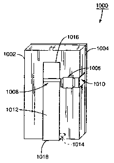
Turning now to Figure 18, a wireless communication device 1000 is illustrated.
Wireless communication device 1000 may comprise a substrate 1002, a ground
plane
1004, a wireless communication chip 1006, a feed line 1008, a chip grounding
line
1010, an antenna 1012, and an antenna grounding element 1014.
In particular, wireless communication device 1000 may be either active or
2o passive as described with reference to U.S. Patents 5,347,280 (previously
incorporated)
and 5,585,953, the latter of which is expressly incorporated by reference.
Substrate
1002 may be almost any time of dielectric material, although polypropylene or
comparable plastics are specifically contemplated.
CA 02518613 2005-09-09
WO 03/092119 PCT/IB03/02272
30 P/63086.WOP5
Ground plane 1004 may be a foil tape, a conductive material secured to
substrate
1002 through other means, or other conductive surface as previously described.
Ground
plane 1004 may cover substantially all of the rear or bottom surface of
substrate 1002.
While in this embodiment, the ground plane 1004 is parallel to the antenna
1012
opposite the antenna 1012, other embodiments below show the ground plane 1004
in the
same plane as the antenna 1012 and it is also possible to position the antenna
1012
perpendicular to the ground plane 1004.
Wireless communication chip 1006 may comprise a device from INTERMEC as
used in their IntellitagC~ labels and those devices from SCS as used in their
DL100 label
to although other devices are certainly possible, especially in light of the
present
invention's suitability to both active and passive wireless communication
devices 1000.
Wireless communication chip 1006 may comprise a control system 12, memory 18,
a
battery, a sensor 20, and other conventional components, as illustrated in
Figure 1.
Feed line 1008 may be a conductive strip with a non-conductive adhesive or
material securing it to substrate 1002 and antenna 1012. The non conductive
material
or adhesive allows feed line 1008 to couple capacitively to antenna 1012
without
creating a short at frequencies at or near DC. Some wireless communication
chips 1006
do not operate with shorts at these low frequencies, hence the need far the
insulation. If
chip 1006 does work with a low frequency short, the insulation of the adhesive
or
2o material may be foregone if needed or desired. The placement, width, and
length of
feed line 1008 controls the impedance matching between wireless communication
chip
1006 and antenna 1012. This structure, and the others presented herein provide
an
acceptably wide bandwidth functionality in a relatively thin and small
structure in close
proximity to the ground plane of the structure. Alternative coupling elements
instead of
CA 02518613 2005-09-09
WO 03/092119 PCT/IB03/02272
31 P/63086.WOP5
feed line 1008 may also be used. These may be added components such as a
surface
mounted capacitor or the like as needed or desired.
Chip grounding line 1010 electrically connects wireless communication chip
1006 to ground plane 1004 and may be made from any appropriate conductive
material.
Antenna 1012 may be formed from any conductive material, such as a foil tape,
or printed, such as through the previously described conductive ink or the
like as needed
or desired. First end 1016 is an open circuit, while second end 1018 is short
circuited to
ground plane 1004 by antenna grounding element 1014. It is further possible in
this,
and the other embodiments presented herein to indirectly connect the second
end 1018
1o to the ground plane 1004 by inductive or capacitive coupling. Note that it
is possible in
the capacitive coupling embodiment just mentioned to position a separate
wireless
communication chip 1006 (not shown) with a non-conducting glue as the
connector
between the antenna 1012 and the ground plane 1004. This may simplify the
assembly
process in certain assembly techniques. It should be appreciated that almost
every
element will have some small impedance and the term "electrically shorted" as
used
herein includes such low impedance resistive or reactive elements. While
antenna
grounding element 1014 is illustrated as a conductive strip wrapping around
the edge,
alternative shorting methods are also contemplated, such as copper plated
through holes,
commonly used in printed circuit board (PCB) processes, or a conductive
material
2o sucked through a hole.
Antenna 1012 may be a quarter wavelength long for the desired operating
frequency. This distance is measured from first end 1016 to second end 1018.
The
actual length will vary on a number of factors, such as the effective length
of the
antenna grounding element 1014 around the edge of the substrate 1002,
thickness of the
CA 02518613 2005-09-09
WO 03/092119 PCT/IB03/02272
32 P/63086.WOP5
substrate 1002, width of the resonant element, dielectric constant of the
substrate 1002,
thickness of the substrate 1002, desired impedance at the coupling point, and
other
factors understood in the art.
In this embodiment, wireless communication chip 1006 is generally
perpendicular to the primary axis of antenna 1012.
In contrast, as illustrated in Figure 19, the elements of wireless
communication
device 1000A remain essentially unchanged, however, the position of wireless
communication chip 1006 has changed so that now chip 1006 is substantially
parallel to
antenna 1012. Also note that ship grounding line 1010 has been extended and
feed line
1008 couples to chip grounding line 1010 instead of the pins of chip 1006 as
illustrated
in wireless communication device 1000.
The main advantage of this approach is that the structure may be simpler to
produce, with feed line 1008 fabricated as a separate label added during
production.
A third embodiment, wireless communication device 1000B, is illustrated in
Figure 20, wherein quarter wavelength antenna 1012 is formed by a length of
Coplanar
Waveguide Ground plane (CPWG) 1020 positioned on the same surface of substrate
1002 as antenna 1012. First end 1016 is still an open circuit, and second end
1018 is
still shorted electrically to ground. Gap 1022 separates antenna 1012 from
CPWG
1020.
2o In CPWG technology, the fields associated with the RF signal are contained
between a central strip (antenna 1012) and two planar areas of ground plane
(1020). A
rear ground plane (not shown) underneath the dielectric is not required but
can be
accommodated. An advantage of this embodiment is that a connection from the
top
surface to the back surface is no longer required, simplifying construction.
CA 02518613 2005-09-09
WO 03/092119 PCT/IB03/02272
33 PJ63086.WOP5
Alternatively, different impedance matching characteristics may be possible
with this
arrangement or certain design parameters may be enabled with this arrangement
Instead of feed line 1008 coupling wireless communication chip 1006 to antenna
1012, an inter digital capacitive structure may be used as illustrated in
Figures 21 and
22. Inter digital capacitive structures include those that have a stub similar
to a finger
(digital) that extends into the general space of another element (inter). The
structures
capacitively couple to one another. A further discussion of inter digital
structures may
be found in IEEE TRANSACTIONS ON MICROWAVE THEORY AND
TECHNIQUES A PUBLICATION OF THE IEEE MICROWAVE THEORY AND
to TECHNIQUES SOCIETY March 2000, Volume 48, Number 03 ACCURATE
CIRCUIT MODEL OF INTERDIGITAL CAPACITOR AND ITS APPLICATION TO
DESIGN OF NEW QUASI-LUMPED MINIATURIZED FILTERS WITH
SUPPRESSION OF HARMONIC RESONANCE by L. Zhu and K. Wu.
In particular, Figure 21 illustrates a wireless communication device 10000
comprising a wireless communication chip 1006 mounted on substrate 1002 and
grounded via chip grounding line 1010. Antenna 1012 is likewise grounded via
antenna
grounding element 1014. In place of feed line 1008, a stub 1024 extends into
the area
of antenna 1012. Gap 1026 allows stub 1024 to couple capacitively to antenna
1012.
Figure 22, in contrast, discloses a wireless communication device 1000D
2o comprising a plurality of stubs 1028 that extend into the area of antenna
1012. The gap,
size and number of inter stubs 1024 or 1028 determines the relative capacitive
cross
coupling between stubs 1024,1028 and antenna 1012. The more circumferential
length
in close proximity increases the capacitance. The narrower the gap between the
elements increases the capacitance. The size of the stubs may affect at which
CA 02518613 2005-09-09
WO 03/092119 PCT/IB03/02272
34 P/63086.W~P5
frequencies the capacitance is maximized. As long as the elements are short in
comparison to a wavelength at the operating frequency the inter digital area's
electrical
characteristics are primarily those of a capacitor.
It should be appreciated that both of these techniques may be used with any of
the techniques described with respect to Figures 18-20.
This method of proving a non-contacting feed line 1008 or stubs 1024 or 1028
has some interesting variants that can give mufti-frequency operation for a
wireless
communication device 1000. For example, consider wireless communication device
1000F disclosed in Figure 23.
In particular, wireless communication device 1000F comprises a substrate 1002
with a rear ground plane 1004. Wireless communication chip 1006 is connected
to
ground plane 1004 by a chip grounding line 1010. Antenna 1012A acts (with
ground
plane 1004) as a half wavelength patch antenna at a first operating frequency,
such as
915 MHz. The operating frequency and dielectric constant of substrate 1002
determine
the dimensions of the square patch.
A short section of CPWG transmission feed line 1008A feeds patch antenna
1012A capacitively at the first frequency but acts as an antenna at a second
frequency,
allowing the device to work efficiently at both frequencies. If increased
capacitance for
the feed is required a inter digital structure with more fingers can be used
either along
2o the entire length of the feed line or at its end. In an exemplary
embodiment, the antenna
1012A is approximately 53 mm to a side allowing operation at 915 MHz, and the
transmission feed line 1008A is approximately 16 mm long allowing operation at
2.45
GHz. Patch antennas are well understood in the antenna art, and are popular
for low
profile applications. They commonly consist of a rectangular metal patch on a
CA 02518613 2005-09-09
WO 03/092119 PCT/IB03/02272
35 P/63086.WOP5
dielectric-coated ground plane. For a further discussion of patch antennas,
reference is
made to U.S. Patent No. 6,140,969, which is hereby incorporated by reference.
This structure can also potentially be used with a 1/4 resonant element, as
shown
in the earlier diagrams. An example of this ability is illustrated in Figure
24. In this
embodiment, in wireless communication device 10006, substrate 1002, ground
plane
1004, and wireless communication chip 1006 remain essentially unchanged as are
chip
grounding line 1010 and antenna grounding element 1014. Feed line 1008B acts
as a
feeding element at UHF, but acts as an antenna at microwave frequencies.
Antenna
1012B acts as an antenna at UHF frequencies and has an open circuit at first
end 1016.
to Construction of one embodiment of these antenna arrangements is illustrated
in
Figures 25-28. A kit 1050, illustrated in Figure 25, for assembling an quarter
wavelength antenna comprises a substrate 1002, a chip component 1052, and a
ground
plane/antenna component 1054. Substrate 1002 may be of any suitable dielectric
material. Chip component 1052 comprises a conductive strip comprising antenna
feed
line 1008 and chip grounding line 1010 coupled to wireless communication chip
1006.
As previously noted, there may be a non-conductive adhesive or material
disposed on
antenna feed line 1008.
Groundplane/antenna component 1054 comprises a conductive material with
ground plane 1004 and antenna 1012, coupled by antenna grounding element 1014.
As illustrated in Figure 26, ground plane/antenna component 1054 is wrapped
around substrate 1002 with groundplane 1004 substantially covering a rear
surface of
substrate 1002 and antenna 1012 being disposed on the opposite surface, A
suitable
adhesive may secure component 1054 to substrate 1002.
CA 02518613 2005-09-09
WO 03/092119 PCT/IB03/02272
36 P/63086. WOPS
Having wrapped ground plane/antenna component 1054 around substrate 1002,
chip component 1052 is then wrapped around the side of substrate 1002. Antenna
feed
line 1008 may be coupled to antenna 1012 and chip grounding line 1010 coupling
chip
1006 to ground plane 1004.
This assembly routine results in an assembled wireless communication device
1000 as illustrated in Figure 28. Exemplary dimensions for the components are
as
follows. For substrate 1002, 63 mm long x 25 mm wide, with the thickness
determined
by the desired operating frequencies. For chip component 1052, a feed line
1008
approximately 10 mm long and a ground line 1010 approximately 20 mm long. For
1o ground plane/antenna component 1054, an antenna 1012 and ground element
1014
approximately 53.5 mm long and having a width of 10 mm. Ground plane 1004 may
be
63 mm long by 25 mm wide. These dimensions provide operation at one desired
frequency, and it should be appreciated that other operating frequencies may
require
different dimensions. They are not intended to be limiting, but rather
exemplary of one
embodiment of the present invention.
Certain modifications and improvements will occur to those skilled in the art
upon a reading of the foregoing description. It should be understood that the
present
invention is not limited to any particular type of wireless communication
device, tabs,
packaging, or slot arrangement. For the purposes of this application, couple,
coupled, or
2o coupling is defined as either directly connecting or reactive coupling.
Reactive
coupling is defined as either capacitive or inductive coupling.
One of ordinary skill in the art will recognize that there are different
manners in which
these elements can provide to accomplish the present invention. The present
invention
is intended to cover what is claimed and any equivalents. The specific
embodiments
CA 02518613 2005-09-09
WO 03/092119 PCT/IB03/02272
37 P/630~6.WOP5
used herein are to aid in the understanding of the present invention, and
should not be
used to limit the scope of the invention in a manner narrower than the claims
and their
equivalents.