Note : Les descriptions sont présentées dans la langue officielle dans laquelle elles ont été soumises.
' CA 02518768 2005-09-12
- 1 - 2004P08915US-Rai
Electronic ballast having a pump circuit for a discharge lamp
having preheatable electrodes
Field of the invention
The present invention relates to an electronic ballast that is
designed for operating lamps having preheatable electrodes.
Background of the invention
Such lamps and ballasts have been known per se for a long time.
Use is made in one group of appliances of a so called PTC
element (a resistor with a decidedly positive temperature
coefficient) for stipulating a preheating time when such a lamp
is restarted. The PTC element is heated up during preheating by
a current and terminates the preheating operation by increasing
its electric resistance.
The control of the converters, in particular of the switching
transistors used therein, can be performed, on the one hand, by
feedback, in which case a so called self-excited converter is
spoken of. On the other hand, it is also known to control
converters externally by means of a sequential control system
and, in the process, particularly to influence the operating
frequency of the converter, for example in order to control the
lamp current in continuous operation.
As a rule, the ballasts are designed for operating on an ac
voltage supply system. A rectifier is used to generate an
intermediate circuit do voltage that is used to supply a
converter which, in turn, generates a supply of power of higher
frequency than the system frequency for the purpose of
operating the lamp.
An important property of such ballasts is the way in which
power is drawn from the ac voltage supply system. When the
CA 02518768 2005-09-12
- 2 - 2004P08915US-Rai
rectifier charges an intermediate circuit storage capacitor,
abrupt charging processes come about in the intermediate
circuit storage capacitor without any further measures when the
instantaneous system voltage is above the capacitor voltage.
This generates line current harmonics and causes a poor power
factor.
There are various possibilities for improving the power factor,
that is to say for reducing the line current harmonics. The
corresponding properties of electronic ballasts are also
covered in part by regulations, for example IEC1000-3-2. In
addition to dedicated converters for charging the intermediate
circuit storage capacitor (or, more generally, main energy
store) from the rectified system voltage, so called pump
circuits also come into consideration. The latter require a
comparatively low outlay on circuitry.
It is inherent in the topology of a pump circuit that the power
rectifier is coupled to the intermediate circuit storage
capacitor via at least one electronic pump switch. This results
in a pump node between the power rectifier and the electronic
pump switch. Said pump node is coupled to the converter output
via a pump network. The pump network can include components
that at the same time can be assigned to a matching network for
coupling the lamp to the converter output. The principle of the
pump circuit consists in withdrawing energy from the rectified
system voltage via the pump node during a half period of the
converter frequency, and buffering it in the pump network. In
the subsequent half period, the buffered energy is fed to the
intermediate circuit storage capacitor via the electronic pump
switch.
Energy is consequently withdrawn from the rectified supply
voltage in step with the converter frequency. In general, the
electronic ballast includes filter circuits that suppress
spectral components of the line current in the region of the
converter frequency and above. The pump circuit or circuits can
CA 02518768 2005-09-12
- 3 - 2004P08915US-Rai
be designed such that the line current harmonics comply with
the abovementioned regulations or other requirements.
As regards pump circuits, reference may otherwise be made to
the prior art, specifically in particular to the applications
DE 103 03 276.2 and DE 103 03 277.0 from the same applicant and
to the citations there.
Summary of the Invention
The invention is based on the technical problem of specifying
an electronic ballast that is improved with regard to the
preheating of lamp electrodes and which has a pump circuit.
The invention is directed to an electronic ballast for a
discharge lamp having preheatable electrodes, which ballast
has:
- an ac voltage supply terminal,
- a rectifier connected to the supply terminal,
- a converter for generating a higher-frequency supply power
for the discharge lamp from the supply power, rectified by
the rectifier, of the supply terminal,
- a pump circuit for improving the power factor of the
ballast by drawing energy from the ac voltage supply
terminal,
characterized in that the ballast includes a preheating
transformer that is designed to supply a preheating power to
the preheatable electrodes, which are connected on the
secondary side to the lamp, doing so during a preheating phase
before said lamp is ignited, the ballast being designed to
operate the converter during preheating with a frequency that
is raised by comparison with the open circuit resonant
frequency of the ballast, in order to supply the primary side
of the preheating transformer, and to a corresponding method
for operating a lamp.
CA 02518768 2005-09-12
- 4 - 2004P08915US-Rai
Preferred refinements of the invention are specified in the
dependent claims and are explained in more detail below. The
disclosure always relates here both to the method category and
to the device category of the invention. The inventor has
proceeded from the fundamental consideration that a pump
circuit continues to constitute a possibility for power factor
correction that is attractive because it is simple and
effective.
He has further looked for a solution in which a sequential
control system is used instead of a PTC element for defining
the preheating phase. The main problem arising here is that the
energy dissipated by the PTC element in the course of the
heating process is eliminated. The energy pumped by the pump
circuit must therefore be dissipated in another way during
preheating. It has been observed that the pump action of the
pump circuit can generally pump more energy than is required
for preheating the electrodes. Components, in particular the
intermediate circuit storage capacitor, can experience
overloading in this case through the voltage rising to
impermissible values.
However, this can be prevented by reducing the pump action of
the pump circuit, specifically in a particularly simple and
efficient way by raising the frequency. Thus, the invention
provides that a substantially higher converter frequency is
used during preheating by comparison with the open circuit
resonant frequency.
Expressed in a simplified way, the lowering of the effective
pump action with the frequency is associated with the fact that
the resonant behavior of the resonant circuit including the
lamp has a frequency dependence that overcompensates the
frequency dependence of the capacitive pumping and inductive
pumping. In approximate terms, the effective pump power is
lowered in a fashion approximately proportional to the
reciprocal of the square of the frequency in the case of
CA 02518768 2005-09-12
- 5 -_ 2004P08915US-Rai
capacitive pump circuits, and in a fashion approximately
inversely proportional to the frequency in the case of
inductive pump circuits.
In particular, the frequency used during preheating can be 1.3
times higher than the open circuit resonant frequency,
frequencies 1.4, 1.5, 1.6, 1.7, 1.8, 1.9 times higher or
approximately at or above two times higher increasingly being
preferred so that the pump action is significantly reduced by
comparison with the operation. The open circuit resonant
frequency is in this case the resonant frequency, usually so
denoted, of the lamp circuit without a lamp connected, which
results in the way generally known essentially from the
inductance of the lamp inductor and the capacitance of the
resonance capacitor.
Finally, the invention provides a preheating transformer with
the aid of which it is possible to generate a current that is
sufficiently strong for preheating. Otherwise, there is the
risk that because of the inductor effect of the lamp inductor,
the current will become too small at the preferred relatively
high preheating frequencies, this rendering it impossible to
attain an adequate preheating effect with regard to the current
(not the energy). The raising of the preheating frequency in
accordance with the invention thus initially counteracts the
generation of sufficiently strong preheating currents. This
problem can be eliminated, however, by means of the
abovementioned preheating transformer.
It can therefore be achieved overall that in the case of
preheating with an electronic ballast having a pu:~p circuit and
without a PTC element, so high a converter freaaency is used
that the preheating energy produced by the converter lies at
most at the maximum permissible preheating energy of the
respective lamp electrodes. Such preheating energies can, for
example, be assigned to each lamp electrode in accordance with
CA 02518768 2005-09-12
- 6 - 2004P08915US-Rai
the energy-controlled preheating in compliance with IEC81 or
IEC901.
Furthermore, the preheating transformer offers a do isolation
relative to the electrodes, which is likewise advantageous in
many instances.
It is possible, overall, to avoid the disadvantages of the
frequently used PTC elements that are, for example, still hot
and of high resistance after relatively short system pauses
such that there is then insufficient preheating of the lamp
electrodes and therefore a deleterious cold start. Furthermore,
PTC elements exhibit losses that on the one hand worsen the
efficiency of the ballast, and on the other hand lead to a
frequently undesired additional heating associated with
correspondingly greater problems with reference to waste heat
and the durability of the components and soldering points.
Furthermore, in the case of more modern lamps (for example T5
design), substantial voltage loads occur in the case of series
circuits, above a11, which likewise can no longer be
implemented directly with PTC elements. Finally, switching off
the pump circuit during preheating is superfluous, and thus
also is the necessity for correspondingly designed switches
and, in particular, for stress-proof driver circuits (high side
drivers).
On the other hand, it is preferred within the scope of the
invention to provide a switch for switching off the preheating
transformer. It is possible thereby after preheating also to
avoid withdrawing energy by the preheating circuit no matter
how small the amount. This is important chiefly whenever the
aim is to operate lamps in the case of which there are
particularly critical requirements with reference to lamp
temperature and the aim is therefore to suppress (cut off) any
sort of additional introduction of heat, for example owing to a
small residual heating current during continuous operation.
When this is not so decisive, or there is another possibility
CA 02518768 2005-09-12
- 7 - 2004P08915US-Rai
for suppressing residual heating currents in continuous
operation, it is preferred to make use of the lamp inductor,
which is present in any case, as primary winding of the
preheating transformer, that is to say provide the lamp
inductor with a few additional windings that are possible with
a very low cost outlay. One possibility of at least reducing
residual heating currents in continuous operation consists, for
example, in switching a capacitor into the preheating circuit,
that is to say on the secondary side of the preheating
transformer. In the case of the raised preheating frequencies
according to the invention, said capacitor has a relatively low
impedance and therefore does not interfere much; however, its
impedance rises in normal operation owing to the frequency
reduction. Such ~a capacitor also has other advantages,
specifically do current blocking. This can be important, for
example, in conjunction with the detection of filament breakage
(not discussed in detail within the scope of this invention),
in the case of which use is made of the ability of the lamp
electrodes to conduct direct current. Here, the secondary
windings lying in parallel in the preheating circuits can
interfere, but would be isolated in terms of direct current by
the capacitor.
A further possibility, which is, however, less preferred within
the scope of this invention for various reasons, consists in
utilizing a resonance in the case of the preheating frequency,
particularly in the preheating circuit itself. However,
problems can also arise in continuous operation owing to
excitation of resonance by harmonics, in which case it has also
to be borne in mind that the voltage characteristics produced
by the converter in continuous operation are regularly not
sinusoidal and therefore rich in harmonics.
In the case of the ballast according to the invention, it is
preferred to provide a lamp current or lamp power control that
varies the converter frequency during continuous operation of
the lamp such that a specific desired value is met. This is
CA 02518768 2005-09-12
- 8 - 2004P08915US-Rai
ultimately performed by bringing the converter frequency nearer
to, or removing it from the resonant frequency of the lamp
resonant circuit including the lamp.
Furthermore, a preferred refinement of the invention provides a
voltage control circuit that is used to set the starting
voltage of the lamp resonant circuit via the frequency of the
converter of the ballast. This voltage control circuit is
advantageous because a relatively accurate setting of frequency
is required when starting via resonance excitation because of
the quality of the lamp resonant circuit. The control circuit
can now match the frequency to the resonance behavior of the
lamp resonant circuit, or "move it subsequently", and, in
particular, in so doing operate by limiting the starting
voltage through varying the frequency.
The previously mentioned control circuit for the lamp current
or power can be combined with the voltage control circuit to
the extent that both access the same control input for
controlling the operating frequency of the converter. It can
preferably be provided in this case that the circuit functions
as a current or power control circuit (that is to say
continuous-operation control circuit) as soon as appreciable
lamp currents flow, that is to say the lamp has started, while
in the other case the voltage regulation "takes precedence".
The abovementioned combination of continuous-operation circuit
and voltage control circuit can, furthermore, be designed in
order to apply the lamp voltage, a potential derived therefrom
or another variable correlating therewith to an input of the
control amplifier or switching transistor of the continuous-
operation control circuit. Of course, it can also suffice to
use only a temporal component of the lamp voltage or of the
correlating variable. The object of this is to deactivate the
continuous-operation control circuit during preheating and
starting until the lamp has switched on and reached its running
voltage. The preheating and starting operations can therefore
CA 02518768 2005-09-12
- 9 - 2004P08915US-Rai
proceed without disturbance, and the continuous-operation
control circuit is used only in continuous operation.
Furthermore, it is preferred to advance relatively quickly to
the ignition after the actual preheating process, that is to
say after the lamp electrodes have reached the required
temperature. Specifically, when the frequency drop then present
results too slowly starting at the preheating frequency, the
overloading of components mentioned at the beginning can occur
even in this transition phase owing to the excessive pump
action of the pump circuit. Transition times of at most 10 ms,
preferably below 8, 6, 4, 2 or 1 ms, have proved themselves
here. It is conventional here to make use, however, of time
intervals of the order of magnitude of 100 ms.
The invention is explained below in more detail with the aid of
exemplary embodiments, the individual features being important,
as already mentioned, both for the device category and for the
method category, and also possibly being essential to the
invention in other combinations, in addition.
Brief Description of the Drawings)
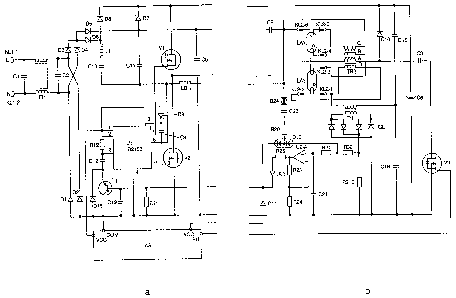
figures la-b show a circuit diagram of a first exemplary
embodiment according to the invention. For
reasons of space, the circuit diagram is split
into figures la and lb. In what follows,
references to figure 1 are understood as a
reference to the respective subfigure la or lb.
figures 2a-b show a circuit diagram of a second exemplary
embodiment according to the invention. For
reasons of space, the circuit diagram is split
into figures 2a and 2b. In what follows,
references to figure 2 are understood as a
reference to the respective subfigure 2a or 2b.
CA 02518768 2005-09-12
- 10 - 2004P08915US-Rai
figure 3 shows actual measurement curves for quantitative
illustration of the second exemplary embodiment.
figure 4 shows actual measurement curves for quantitative
illustration of the second exemplary embodiment.
Detailed description of the Invention
Figure 1 shows a first exemplary embodiment. Drawn in at the
left are two terminals KL1-1 and KLl-2 to which a system
voltage is to be connected. A filter composed of two capacitors
Cl and C2 and two coupled coils denoted by F11 connects the
system voltage terminals to a full bridge rectifier composed of
the diodes Dl-D4. A pump circuit has two pump branches that
include diodes D5-D8 via which the rectified supply voltage is
applied to an intermediate circuit storage capacitor C6, which
is depicted at the far right in the figure.
The intermediate circuit capacitor C6 feeds the converter,
which is constructed here as a half bridge composed of two
switching transistors Vl and V2. By being clocked appropriately
in phase opposition, the half-bridge transistors Vl and V2
generate at their center tap an ac voltage that oscillates
between the two potentials of the rectifier output. This ac
voltage is connected to the supply branches via a lamp inductor
LDl and, in the present case, a series circuit of two discharge
lamps LA1 and LA2 and a measurement transformer TRl, explained
in still greater detail below, via two coupling capacitors C15,
C16.
Figure 1 shows that not only a current can flow through the
discharge plasma in the lamps LA1 and LA2, but that also a
preheating current can flow through the upper electrode of the
upper lamp LA1, the lower electrode of the lower lamp LA2, the
two interconnected electrodes of the lamp LAl and the lamp LA2,
CA 02518768 2005-09-12
- 11 - 2004P08915US-Rai
and a respective secondary winding of a heating transformer
TR2.
In order to meet relevant regulations with reference to line
current harmonics, for example IEC 1000-3-2, use is made here
of a pump circuit having two pump branches and which proffers a
comparatively low outlay on circuitry. In principle, the
rectifier is coupled here to the main energy store, the
intermediate circuit storage capacitor C6, via an electronic
pump switch D6/D8 or D5/D7. The pump nodes lying between the
diodes D5 and D7, and D6 and D8, are coupled via a pump network
to the output of a converter or inverter that is explained in
more detail later. Consequently, during a half period of the
inverter frequency, energy is drawn from the system voltage via
the pump nodes and buffered in a pump network. In the half
period following thereupon, the buffered energy is fed to the
intermediate circuit storage capacitor C6 via the electronic
pump switch, here the diodes D8 and D7. Energy is thereby
withdrawn from the system in time with the inverter frequency.
The abovementioned filter elements largely suppress higher
spectral components, and so line current is ultimately consumed
in a quasi-sinusoidal fashion.
The details of the pump circuit are not important for the
present invention. Reference is made here to the prior art and,
in particular, to the applications DE 103 03 276.2 and
DE 103 03 277.0 from the same applicant. What is important is
that the pump branches can pump energy into the circuit with
each period of the inverter, but cannot return it.
In addition to the already mentioned lamp inductor LD1, the
lamp resonant circuit has resonance capacitors C5 and C9.
The lamp resonant circuit is used firstly to raise the voltage
by means of an excitation close to resonance. After ignition,
the lamp resonant circuit secondly acts as a matching network
CA 02518768 2005-09-12
- 12 - 2004P08915US-Rai
that transforms the output impedance of the inverter into an
impedance suitable for operating the discharge lamps.
Otherwise, the lamp resonant circuit also acts as a pump
network. If the voltage at the pump nodes already mentioned is
lower than the instantaneous system voltage, the pump network
draws energy from the system. In the inverse case, the energy
drawn is output to the intermediate circuit capacitor C6. A
further pump action proceeds from the capacitor C8. The
capacitor C8 acts as a so called trapezoidal capacitor for
relieving the switching load on the half-bridge transistors V1
and V2. The pump network for the second pump branch comprises a
series circuit of a pump inductor L1 and a pump capacitor C10.
The half-bridge transistors Vl and V2, which are designed as
MOSFETs, are driven at their gates by an integrated driver
circuit, for example International Rectifier type IR2153. This
IC also includes a high side driver for driving the ~~high"
half-bridge transistor Vl. The diode D9 and the capacitor C4
are provided in this context.
Apart from the driver circuits for the half-bridge transistors
Vl and V2, the IC includes an oscillator whose frequency can be
set via the terminals 2 and 3 (RT and CT). The frequency in
accordance with RT and CT corresponds to the lowest operating
frequency of the half bridge. A frequency-determining resistor
R12 is connected between the terminals 2 and 3. Connected
between the terminal 3 and the lower supply branch serving as
reference potential is a frequency-determining capacitor C12,
and connected in series therewith is the emitter-collector path
of a bipolar transistor T3. A diode D15 is connected in
parallel with the emitter-collector path in order to be able to
charge and discharge C12. The half-bridge frequency can be set
by means of a voltage between the base terminal of the bipolar
transistor T3 and the reference potential, and thereby forms a
manipulated variable for a control loop. The base terminal of
the bipolar transistor T3 is driven by circuit parts depicted
CA 02518768 2005-09-12
- 13 - 2004P08915US-Rai
further right in figure 1. The bipolar transistor and the IC as
well as the associated wiring therefore form a controller.
The functions of the IC and the associated wiring can also be
implemented by any desired voltage- or current-controlled
oscillator circuit that accomplishes the drive of converter
transistors via driver circuits. Otherwise, the inverter
described is controlled by a sequential control system AS that
is depicted at the bottom in figure 1.
In the exemplary embodiment, the controller acquires the lamp
current as controlled variable, specifically the discharge
current, to put it more precisely. The latter is acquired via a
measurement transformer TR1. A further known lamp current
measurement that can also be applied could be performed via one
of the two coupling capacitors C15, C16 or a component thereof
acquired on a measuring shunt. A full-bridge rectifier GL
rectifies the current and leads it to the reference potential
via a low-resistance measuring shunt R21D. The voltage drop
across R21D is entered into the input of a non-inverting
measuring amplifier in the form of an operational amplifier
U2-A via a lowpass filter composed of the resistor R21 and the
capacitor C21, which serves for averaging. This measuring
amplifier is connected in a known way by the resistors R23-R25
and passes its output signal to the controller input
(manipulated variable node) described via the diode D23. This
closes the current control loop which was denoted previously as
the continuous-operation control circuit. The diode D23 in this
case decouples the output of the measuring amplifier U2-A from
the voltage divider D24, C20, R20, D16, R11, when the potential
at the tie point LD1-D24 is sufficiently high. According to the
invention, the circuit arrangement is designed in this case
such that without a discharge current the voltage at the anode
of the diode D23 assumes a value defined by the output VCO of
the sequential control system AS via a diode D11, that is to
say the sequential control system AS determines the start
frequency.
CA 02518768 2005-09-12
- 14 - 2004P08915US-Rai
The sequential control system AS thus stipulates via the output
VCO a frequency value that is more than double the open circuit
resonant frequency.
The inverter is therefore operated at a prescribed preheating
frequency and is applied correspondingly to the primary winding
A of the preheating transformer TR2. Consequently,
corresponding preheating currents flow into the secondary
windings B, C and D.
In this arrangement, the capacitor C3 serves for setting an
average voltage between the voltages across the intermediate
circuit storage capacitor C6 as reference potential for the
right-hand terminal for the primary winding A.
After a preheating time prescribed by the sequential control
system AS, the sequential control system AS goes over into the
ignition mode within approximately 1 ms and generates the
required starting voltage by means of resonant amplification in
the lamp resonant circuit. The preheating circuits can be
switched off simply after preheating by means of the switch V3
that is in series with the primary winding A of the preheating
transformer TR2 and can be controlled via the output PH of the
sequential control system AS. Any further dissipation of energy
in the preheating circuits is thereby suppressed in common with
an unnecessary introduction of heat into the lamps LRl and LR2
by the electrodes.
Since the starting phase for the half-bridge switches VI and V2
and the lamp resonant circuit (LD1, C5, C9) which follows the
preheating constitutes a high load, a protective circuit is
provided here for avoiding excessively high starting voltages.
However, this protective circuit simultaneously also forms a
voltage control circuit for setting the starting voltage to a
suitable value. This purpose is served by a suppressor diode
D24 at the lamp-side terminal of the lamp inductor LDl. It will
CA 02518768 2005-09-12
- 15 - 2004P08915US-Rai
also be possible here to use a metal oxide varistor or a zener
diode instead of a suppressor diode. It is therefore a
threshold switch that is involved. The threshold switch, which
here lies in the high voltage range, can, however, also be
omitted, and an appropriate threshold circuit can be provided
in the low voltage range, that is to say in the range of the
evaluation. This is not depicted here, but is immediately clear
to the person skilled in the art.
Via a series circuit having a capacitor C20 and a resistor R20,
the lamp voltage is given starting from a specific threshold
value between two diodes D16. The anode of the left-hand diode
constitutes a second control input. The value of the resistor
R20 influences the level of influence of the intervention in
the control loop, which is outlined below.
The lamp voltage tapped via the suppressor diode D24 forms a
measure of the reactive energy oscillating in the lamp resonant
circuit, and of the starting voltage. If this voltage exceeds
the threshold value of the suppressor diode D24, the half-
bridge frequency is raised, and the reactive energy oscillating
in the resonant circuit is thereby reduced, and on the other
hand the lamp voltage is diminished.
A typical value for the threshold of the suppressor diode D24
is 250 V, for example. The voltage control circuit then exerts
control above this voltage.
Rfter ignition, a lamp current flows that raises the potential
of the anode of the diode D23 to a value that is in the
operating range of the bipolar transistor T3, and thereby
closes the control loop of the continuous-operation control
circuit (for the lamp current).
On the other hand, in the case of a lamp voltage lying above
the threshold value of the suppressor diode D24, the voltage at
the positive input of the control amplifier U2-A is raised via
CA 02518768 2005-09-12
- 16 - 200~P08915US-Rai
the right-hand diode D16, which drives a tap between the
resistors R22 and R32 at said input. The continuous-operation
control circuit can thereby be rendered inoperative when a
starting attempt is being made. This is a factor o~ interest in
order not to permit any disturbances during starting. For
example, in the exemplary embodiment outlined the control of
the lamp current, that is to say the continuous-operation
control circuit, operates with a time constant of the order of
magnitude of 1 ms. On the one hand, with this setting the
substantially faster converter frequencies are adequately
filtered, while on the other hand the control is thereby
approximately one order of magnitude faster than the 100 Hz
modulation, unavoidable owing to the rectified system voltage,
of the intermediate circuit voltage across the storage
capacitor C6. However, under poor conditions, v~n particular
with older lamps, a starting burst exceeding 1 ms may be
required in order to achieve reliable starting. It is thus then
an advantage to switch off the current control.
By applying a (negative) component of the high lamp voltage via
the components D24, C20, R20, D16 to the non-inver~ing input of
the control amplifier U2-A, the continuous-operation control
circuit is blocked in this case such that the voltage control
circuit already described remains operative.
Figure 2 shows a second exemplary embodiment for which the
explanations relating to the first exemplary er~.aodiment are
largely valid. The same reference symbols are entered for
identical or corresponding parts.
The differences are as follows: for the purpose of
simplification, the lamp inductor LDl and the preheating
transformer TR2 from figure 1 are combined here. The lamp
inductor LDl thus corresponds to the primary wincing A of the
preheating transformer. Its function otherwise remains
unchanged, but it can no longer be switched off, t~at is to say
the switch V3 and the corresponding control ou~put PH from
CA 02518768 2005-09-12
- 17 - 2004P08915US-Rai
figure 1 are absent. As a consequence of the unification of the
primary winding and the lamp inductor, it would also be
possible, specifically, for the preheating circuits to be
switched off only on the secondary side, and this would be
complicated because of the participating voltages and the
corresponding effects on the driver circuits required. Instead
of this, the individual preheating circuits each include a
capacitor C7, C11 and C13, respectively. Said capacitor has the
function already outlined earlier of forming a higher impedance
in continuous operation than during preheating. Furthermore,
the capacitors C7, C11 and C13 for a filament breakage
detection (not depicted here) have, owing to the do
conductivity, the advantage of do disconnection despite
secondary windings B, C and D lying in parallel with the
electrodes. Moreover, this last-named function can also be
implemented in the case of the exemplary embodiment from
figure 1, in which case it would also be possible to use diodes
instead of the capacitors.
The first exemplary embodiment has the advantage of a complete
disconnection of the preheating circuits, and is therefore
especially suitable for particularly efficiency-optimized lamps
that are sensitive to the introduction of heat with regard to
their efficiency. The second exemplary embodiment from figure 2
is particularly simple and cost effective because in fact only
three capacitors (which are, however, optional in any case) and
three additional windings on the lamp inductor are required.
The invention may be illustrated with a few quantitative data
with the first exemplary embodiment (figure 1). Two 36 W
tubular fluorescent lamps are operated in this example, the
elements determining the pump effect being dimensioned as
follows:
LD1 = 1 mH
Ll = 1.8 mH
C5 = 10 nF
C9 = 14 nF
CA 02518768 2005-09-12
- 18 - 2004P08915US-Rai
C10 = 220 nF
C15 = C16 = 100 nF.
The lamp current actually oscillating at the operating
frequency in continuous operation is shown by the surface
(channel 3) filled by hatching in figure 3. Here, the lamp
current has a root-mean-square value of approximately 335 mA
given nominal conditions of 230 V supply voltage at 50 Hz.
Channel C, that is to say the continuous black line, shows the
operating frequency fluctuating between a minimum value of
approximately 47.3 kHz and a maximum value of approximately
61.5 kHz. The fluctuations originate from the lamp current
control via the operating frequency. The remaining fluctuations
in the lamp current are caused, inter alia, by the time
constant of the control.
The open circuit resonant frequency (determined by LD1 and C9)
is at 42.6 kHz, and the starting frequency (given an open-
circuit voltage of 700 V) is approximately 48 kHz.
Figure 4 shows, using the channel B, represented by hatching,
the characteristic of the intermediate circuit voltage U~6 in
the vicinity of a starting process. The preheating frequency
here is 98.5 kHz, that is to say more than double the open
circuit resonant frequency.
It is well in evidence that the intermediate circuit voltage
U~6 does not exceed the peak value of the system voltage
(approximately 325 V) until after the starting in the middle of
the diagram, which can be detected from the lamp current
represented in channel C, and before that remains below this
amplitude. The lamp current in channel C of figure 4
corresponds to channel 3 in figure 3.