Note : Les descriptions sont présentées dans la langue officielle dans laquelle elles ont été soumises.
CA 02519339 2008-05-15
= WO 2004/094098 PCT/US2004/006725
SINTER-BONDED DIRECT PIN CONNECTIONS FOR INERT ANODES
Field of the Invention
[0001] This invention relates to low resistance electricaI connections between
a solid
metallic pin conductor and the interior of a ceramic or cermet inert anode
used in the
production of metal, such as aluminum, by an electrolytic process.
Background of the Invention
[0002] A number of metals including aluminum, lead, magnesium, zinc,
zirconium,
titanium, and silicon can be produced by electrolytic processes. Each of these
electrolytic
processes employs an electrode in a highly corrosive environment.
[0003] One example of an electrolytic process for metal production is the well-
known
Hall-Heroult process producing aluminum in which alumina dissolved in a molten
fluoride
bath is electrolyzed at temperatures of about 960 C-1000 C. As generally
practiced today,
the process relies upon carbon as an anode to reduce alumina to molten
aluminum. The
carbon electrode is oxidized to form primarily C02, which is given off as a
gas. Despite the
common usage of carbon as an electrode material in practicing the process,
there are a
number of disadvantages to its use, and so, attempts are being made to replace
them with
inert (not containing carbon) anode electrodes made of for example a ceramic,
metal-ceramic
"cermet" or metal containing material.
[0004] Ceramic and cermet electrodes are inert, non-consumable and
dimensionally
stable under cell operating conditions. Replacement of carbon anodes with
inert anodes
allows a highly productive cell design to be utilized, thereby reducing costs.
Significant
environmental benefits are achievable because inert electrodes produce
essentially no C02 or
fluorocarbon or hydrocarbon emissions. Some examples of inert anode
compositions are
found in United States Patent Specification Nos. 4,374,761; 5,279,715;
6,126,799; 6,372,119;
6,416,649; 6,423,204; and 6,423;195, all assigned to Alcoa Inc.
[0005] Although ceramic and cermet electrodes are capable of producing
aluminum
having an acceptably low impurity content, they are susceptible to cracking
during cell start-
up when subjected to temperature differentials on the order of about 900 C-
1000 C. In
addition, ceramic components of the anode support structure assembly are also
subject to
damage from thermal shock during cell start-up and from corrosion during cell
operation.
One example of an inert anode assembly for an aluminum smelting cell is shown
in Fig. 3 of
CA 02519339 2005-09-15
WO 2004/094098 PCT/US2004/006725
2
United States Patent Application Publication 2001/0035344 Al (D'Astolfo, Jr.
et al.) where
cup shaped anodes can be filled with a protective material and then attached
to an insulating
lid or plate.
[0006] Making a low resistance electrical connection between a ceramic or
ceramic-
metallic electrode and a metallic conductor has always been a challenge. The
connection
must be maintained with good integrity (low electrical resistance) over a wide
range of
temperatures and operating conditions. Various attempts have been made with
brazing,
diffusion bonding, and mechanically connecting with limited success. Examples
of sinter
threading and electromechanical attachment are shown, for example, in United
States Patent
Specification Nos. 4,626,333 and 6,264,810 B1 (Secrist et al., and Stol et al.
respectively).
Also, differential thermal growth between the pin and ceramic or cermet, over
the assembly
and process temperature range can cause the inert material to crack and/or the
electrical
connection to increase in resistance; rendering the assembly unfit for
continued use.
[0007] What is needed is a pin-to inert material interior connection that is
simple, not
labor intensive to assemble and which will provide a low electrical resistance
connection that
will not deteriorate over time or cause cracking of the anode. It is a main
object of this
invention to provide a low electrical resistance connection of the pin
conductor and inert
anode electrode. It is another object to reduce assembly costs and provide a
simplified design
and method.
Summary of the Invention
[0008] The above needs are met and objects accomplished by providing, a
sintered
electrode assembly comprising: an inert electrode containing a sealed metal
conductor, the
conductor having a surface feature to aid in bond formation, where the
conductor is directly
contacted by and is substantially surrounded by the inert electrode. No metal
foam or metal
powder is needed in this invention to achieve good bonding. The invention also
resides in a
sintered electrode assembly comprising: an inert electrode having a hollow
interior with a top
portion and interior bottom and sidewalls; a metal pin conductor having bottom
and side
surfaces, disposed within the hollow electrode interior and directly
contacting the electrode
interior walls with the aid of a surface feature on the conductor to aid in
bond formation.
There is no need for a seal surrounding the metal pin conductor at the top
portion of the
electrode. This surface feature can be a textural, chemical/mechanical
(including
mechanical/electrical) surface feature or an internal or external flux
feature, and the like and
the term "surface feature" is herein meant to include all of the above.
CA 02519339 2005-09-15
WO 2004/094098 PCT/US2004/006725
3
[0009] The inert electrode is preferably selected from the group consisting of
a
ceramic or a cermet inert anode, and the metal pin conductor is selected from
the group
consisting of nickel, nickel alloy, Inconel, copper, copper alloy, or a
corrosion protected steel,
preferably having a circular cross-section. The surface feature can be an
additive/coating and
is preferably a layer selected from the group consisting of nickel, nickel-
copper alloy, copper,
copper alloy, tin alloy, silver or silver alloy, which has been pre-applied to
the metal pin
conductor by means of a spray coating, dip coating, paint coating or wrapping.
A surface
coating of a flux material, pre-applied or which migrates to the interface
between the
conductor and the anode during sintering is also possible. The anode assembly
is useful for
an electrolytic cell.
[0010] The invention also resides in a method of producing an electrode
assembly
comprising: (1) providing an inert anode electrode having a hollow interior
with a top portion
and interior and bottom and sidewalls; (2) providing a metal pin conductor
having a surface
feature on the surface of or within the conductor; (3) inserting said
conductor into said inert
electrode, and (4) sintering to achieve a chemical/mechanical connection,
where, during the
sintering the surface feature aids bonding.
[0011] The preferred metal pin conductor can be inserted at ambient
temperatures.
The assembly is then sintered and a mechanical-electrical bond is forrned as
the electrode
material shrinks around the metal pin.
[0012] The preferred connection design alleviates cracked anodes due to
differential
thermal growth, provides a stable electrical joint resistance that does not
degrade with age,
and requires only a coating between the pin and ceramic or cermet. This allows
reduced
materials and assembly costs and supports simplified automated assembly.
Brief Description of the Drawings
[0013] A full understanding of the invention can be gained from the above and
following description when read in conjunction with the accompanying drawings
in which:
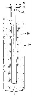
[0014] Fig. 1 is a cross-sectional view of one embodiment of an inert anode
assembly
showing the green anode 10 before sintering, with a metal pin conductor 20,
having an
external surface additive, preferably a bond-coating 30 on the pin surface,
where the pin is,
inserted within the anode. There is a gap 35 between the pin outside diameter
50 and the
green anode inside diameter 40;
CA 02519339 2005-09-15
WO 2004/094098 PCT/US2004/006725
4
[0015] Fig. 2 is a cross-sectional view of the densified inert anode assembly
of Fig. 1
after sintering, showing the intimate bond at interface 45 between the
conductor and sintered
anode;
100161 Fig. 3 is a cross-sectional view of another embodiment of an inert
anode
assembly showing the green anode 60 before sintering, with a bond-coated metal
pin
conductor 70 pressed into the green anode body 60;
[0017] Fig. 4 is a cross-sectional view of the densified inert anode assembly
of Fig. 3
after sintering, showing the intimate bond at interface 45 between the
conductor and sintered
anode;
100181 Fig. 5 is a cross-sectional view of another embodiment of an inert
anode
assembly showing a green anode 80 having a top cavity 85 before sintering, and
preferably a
bond/flux coated metal pin conductor 90 inserted within the anode 80; and
[00191 Fig. 6 is a cross-sectional view of the densified inert anode assembly
of Fig. 5
after sintering, in which the pin material 100 has melted into the cavity 85
and internal
migrational flux material and/or external flux material, shown as dots 120 has
helped
establish an intimate bond at interface 45 between the conductor and sintered
anode.
Detailed Description of Preferred Embodiments
[0020] The metal pin conductor-inert anode connection shown in Figs. 1-6 can
be
made in at least three ways: In the first embodiment, shown in Figs. 1-2,
generally, a hole is
cast or green machined into the ceramic body 10 during fabrication. Then a
specially
designed metallic conductor 20 is inserted into the hole, with a calculated
clearance. The
hole is sized such that during sintering, the ceramic body will shrink around
the conductor
rod, as shown in Fig. 2, providing a well protected, strong connection at
interface 45. The
metallic conductor in cases shown in Figs. 1-6, may be constructed with
"surface feature" 30,
on the conductor defined as one, or a combination, of a non-smooth surface
features, such as
longitudinal grooves or screw threads to provide better adherence of the
ceramic around the
part; or in cases shown in Figs. 1-6, a metallic alloy material, in the form
of a sprayed, dipped
or painted coating, wire or ribbon wrapping, applied around the outside of the
conductor rod,
or internal or external flux material, to provide a bond coating/layer between
the metal and
cermet or ceramic materials to enhance the electrical connection. The coating
is good for all
the Figs. shown. The wire or ribbon wrapping is best for Figs. 3-4. The total
thickness of
male threads, coating, wire, ribbon, or the like "surface feature" after
sintering will range
from about 0.1 to 50 mils (0.00025 to 0.127 cm) preferably 10 to 30 mils
(0.025 to 0.076 cm).
CA 02519339 2005-09-15
WO 2004/094098 PCT/US2004/006725
This material is preferably a metal consisting of a copper, nickel, tin,
silver, palladium,
platinum or an alloy thereof, which melts at the appropriate temperature,
usually between
about 1050 C and about 1450 C during the sintering process, to effect the
interface bond.
[0021] In the second embodiment, shown in Figs. 3-4, generally, the coated
metallic
conductor 70 with surface additive 30 is pressed into the ceramic body 60
before sintering.
The whole part is then sintered together as shown in Fig. 4. In this case,
there is no clearance
between the conductor and ceramic and a strong connection at the interface 45
is still
achieved. Similar surface preparation as in the first embodiment is used.
[0022] In the third embodiment, shown in Figs. 5-6, generally, the ceramic
body is
prepared in the same way, with an oversized hole. This time, a solid low
melting metallic
conductor 90, having a melting point of from about 1050 C to about 1450 C,
such as pure
copper, nickel, or copper-nickel alloy, is inserted into the hole before
sintering. The
conductor rod can have a coating of flux 120 on its surface or which is within
the rod and will
migrate to the surface effective to improve contact with the ceramic of the
inert anode and
provide a surface additive in the form of flux 120 or the like, and may
decrease surface
tension and may allow some metal micro permeation/penetration into the ceramic
surface
pores. This flux type 120 surface additive is shown as dots on the conductor
surface or
gravitating to the surface in Figs. 5-6. This may also be accomplished by
providing flux
interior to the conductor which flux which tends to exit the metal upon
melting, forming an
initial coating on the ceramic improving metal permeability. Useful flux
materials, that is
materials which can/may promote flow and fusing into the ceramic can include,
for example
Sn, Ag and other effective fluxes. The conductor rod melts during sintering,
but is contained
within the hole, providing a continuous, well conformed joint at the interface
45 between the
ceramic body and conductor. The top of the conductor and a metal pool in the
cavity 85 at
the top of the anode may be machined to accept an extension to bring the
current from the
source to the anode. In the above embodiments, it may be desirable to design
the metal
conductor using an outer pipe composed of a stronger material, such as Inconel
or steel to
provide structural integrity and oxidation resistance, with a more
electrically conductive
material, such as copper filling the inside. In the proposed connection
technique, a
connection is achieved during the sintering process, and little or no post-
machining is
required. The connection is also capable of providing both electrical contact
and mechanical
support.
CA 02519339 2005-09-15
WO 2004/094098 PCT/US2004/006725
6
[0023] For convenience, this invention will be described in more detail than
above,
with reference to an electrode assembly for producing aluminum by an
electrolytic process.
As used herein, the term "inert anode" refers to a substantially non-
consumable, non-carbon
anode having satisfactory resistance to corrosion and dimensional stability
during the metal
production process. This can be a ceramic or cermet (ceramic/metal) material,
both of which
are well known in the art. Initial porosity of inert anodes powder is reduced
to 40 vol.%
porosity (60 vol.% of theoretical density) after isostatic or other
pressing/molding possibly
around a mandrel or the like to form a "green" anode. Upon sintering at about
1150 C to
about 1500 C, preferably 1200 C to 1400 C, the ceramic powder consolidates to
from about
1 vol.% to 10 vol.% porosity (90 vol.% to 99 vol.% of theoretical density).
[0024] The metal conductor is usually of a pin/rod design having a circular
cross-
section as shown in Fig. 1. Here, the conductor rod is made smaller than the
hole in the green
anode before sintering. The gap is carefully sized such that during sintering,
said gap closes
and the anode material comes into contact with the metal conductor pin and
surface additive
30. The additive bond coat or wrapping on the pin softens or melts at a
temperature,
achieved during the sintering process, such that it becomes a bonding agent
between the
metal conductor and anode at interface 45, shown in Fig. 2. The gap 35 between
the inert
anode and the metal pin conductor is selected to provide complete interference
fit after
sintering. The anode material does not crack due to the stresses imparted to
it from the metal
pin because of the compliance and ductility of the anode material at the
sintering temperature.
The gap 35 between the inert anode and the metal conductor pin can range from
nearly zero
to 30 mm. Once the connection is achieved at the highest sintering
temperatures, somewhere
between about 1200 C to 1500 C, both metal pin and anode shrink together
during the cool
down process to provide a reduced, highly densified anode, as shown in Fig. 2,
and also Figs.
4, and 6. In all cases the metal pin material is selected to have a higher
coefficient of thermal
expansion (CTE) than the sintered anode material that is about 2% to 50%
higher. The usual
coefficient of expansion of inert anode material is, very generally, from
about 8 to 30 x 10-6
per degree Celsius ( C). In this way, very importantly, no stress is added to
the anode
material during cool down. Some minor disengagement may occur between the pin
and
anode during cool down, but this has been shown not to affect the quality of
the connection.
Over about a 50% higher CTE the disengagement may become a problem. In any
case,
during operation of the anode in electrolysis cells at high temperatures, the
gap is
substantially closed again.
CA 02519339 2005-09-15
WO 2004/094098 PCT/US2004/006725
7
[0025] In the second embodiment shown in Fig, 3-4, the metal conductor pin 70,
with
surface additive 30, is directly compression pressed into the green anode 60
before sintering.
In this case, there is not a gap between the pin and the anode. The compliance
and ductility
of the anode material as it sinters completely absorbs the energy of
interference with the pin
during shrinkage, such that the anode does not crack.
[0026] In the third embodiment Fig. 5-6, the metal pin material 90 is selected
to have
a melting temperature below the ultimate sintering temperature of the anode
80. In this case,
no stress is imparted to the anode material at all during sintering. The
dimensions of the
initial hole in the anode are sized such that after shrinking is complete; the
metal provided
completely fills the cavity including part of top cavity 85. The top surface
of the metal may
have to be machined to a smooth surface 110 in order to attach an extension
piece of the
desired length. As mentioned previously, a flux material 120 either from the
interior of the
metal or as an initial coating on the surface of the pin 90 provides a surface
additive at the
interface 45.
EXAMPLE 1
[0027] An electrode assembly was prepared using a hollow inert anode, a metal
conductor comprised of Inconel 600 alloy, and a coating on the conductor of a
copper-nickel
alloy. The anode was isostatically pressed from powder to have a hollow
opening of 0.813
inches (2.06 cm) diameter. Anode porosity after pressing was about 40 vol.%.
The pin
diameter was 0.75 inches (1.9 cm) and the surface additive coating was applied
as a flame
spray to a thickness of 0.030 inches (0.076 cm) around the pin. The coating
composition was
67.8 wt.% copper, 30.6 wt.% nickel with the balance Fe, Mn, Ti and other
impurities. The
anode was sintered at 1250 C in an argon atmosphere until a full density,
about 1 vol.% to 5
vol.% porosity, was achieved. The concurrent shrinkage allowed the sintered
anode material
to come in contact with the pin and coating and establish a continuous,
coherent electrical
contact at the interface. The bonding was good enough to serve as a mechanical
support.
Final anode dimensions were 6 inches (15.24 cm) long by 3 inches (7.62 cm) in
diameter,
with a hemispherical bottom.
[0028] A group of 12 of these anodes were arranged in an assembly consisting
of a
square array on 4.2-inch (10.6 cm) centers. The anodes were set in an
externally heated cell
with a graphite crucible and an alumina inner sidewall liner. Bath and
aluminum metal were
pre-charged as solid materials, and the anode assembly was mounted above the
bath. Cell
and anodes were preheated simultaneously to an operating temperature of
approximately
CA 02519339 2005-09-15
WO 2004/094098 PCT/US2004/006725
8
960 C. Once the bath and metal were molten, the anodes were lowered into the
bath at an
immersion level of 3.25 inches (8.2 cm), and DC current was applied.
Approximately 1086
amperes total, or 90.5 amperes per anode of DC current was applied. The cell
was
continuously fed with alumina to maintain alumina concentration about 6%. The
cell was
operated for 334 hours under stable conditions. Average cell voltage was 4.77
volts, and was
stable to slowly falling throughout the test, and ranged from 5.3 to 4.5
volts. After the test,
the anodes and cell were slowly cooled. Inspection of the anodes afterwards
revealed that
they were in excellent condition with no cracking and minimal wear.
EXAMPLE 2
[0029] A series of 24 anodes were produced and tested in a statistically
designed
matrix of experiments. The electrode assemblies were prepared using hollow
inert anodes, a
metal conductor, and an additive coating on the conductor. The conductor
comprised a
copper-nickel alloy. The anode was isostatically pressed from powder to have a
hollow
opening of various diameters. The coating composition was 67.8 wt.% copper,
30.6 wt.%
nickel with the balance of Fe, Mn, Ti and other impurities. The anodes were
sintered at
1250 C in an argon atmosphere until a full density was achieved, about 1 vol.%
to 5 vol.%
porosity. The concurrent shrinkage allowed the sintered anode material to come
in contact
with the pin and coating and establish a continuous, coherent electrical
contact at their
interface. The bonding was good enough to serve as a mechanical support. Final
anode
dimensions were 6 inches long (15.24 cm) by 3 inches (7.62 cm) in diameter,
with a
hemispherical bottom.
[0030] The anodes were isostatically pressed from powder to have a hollow
opening.
Variables included the gap between the pin and green anode, the pin material,
the pin
diameter, and the coating thickness. Three levels of gap were produced, such
that the final
calculated radial interference was 10, 20 and 30 mils (0.025, 0.050 and 0.15
cm respectively).
The pin material was varied between Inconel 600 and nickel. The pin diameter
was varied
between 0.75 and 1.5 inches (1.9 and 3.8 respectively). The coating was a
copper-nickel
alloy applied by flame spray, and was varied between 5 and 30 mils (0.013 and
0.15 cm
respectively).
[0031] Each electrode assembly was tested under electrolysis conditions to
determine
the resulting resistance. The electrode assemblies were tested one at a time.
Each was set in
an externally heated cell with a graphite crucible and an alumina inner
sidewall liner. Bath
and aluminum metal were precharged as solid materials and the anode assembly
was
CA 02519339 2005-09-15
WO 2004/094098 PCT/US2004/006725
9
mounted above the bath. Cell and anodes were preheated simultaneously to an
operating
temperature of approximately 960 C. Once bath and metal were molten, the
anodes were
lowered into the bath and DC current was applied. Current was varied from zero
to 120
amperes to allow the calculation of resistance, as shown in Table I below.
Test Radial Interference Pin Material Pin Diameter Additive Resistance in
mils inch Coating m92 (milli
thickness ohms)
mils
1 10 Inconel 0.75 5 23.16
2 20 Inconel 0.75 5 20.79
3 30 Inconel 0.75 5 22.52
4 10 Nickel 0.75 5 23.71
20 Nickel 0.75 5 20.73
6 30 Nickel 0.75 5 20.11
7 20 Inconel 1.5 5 20.43
8 30 Inconel 1.5 5 20.13
9 10 Nickel 1.5 5 19.82
20 Nickel 1.5 5 21.97
11 10 Inconel 0.75 30 22.11
12 20 Inconel 0.75 30 21.57
13 10 Nickel 0.75 30 23.06
14 20 Nickel 0.75 30 19.73
30 Nickel 0.75 30 20.13
16 10 Inconel 1.5 30 22.32
17 20 Inconel 1.5 30 20.57
18 30 Inconel 1.5 30 Did not bond
well
19 10 Nickel 1.5 30 21.89
20 Nickel 1.5 30 21.7
21 30 Nickel 1.5 30 21.35
The data indicates that there is little difference between the Inconel 600 and
the nickel pin
materials. Likewise, the diameter of the pin may vary between 0.75 and 1.5
inches (1.9 and
3.8 cm respectively) with little effect. Additive coating thickness can also
be varied between
5 and 30 mils (0.013 and 0.15 cm respectively) with no detrimental effect in
almost all trials
except Test 21 with Inconel, high interference and thick additive coating. The
cell resistance
was, however, slightly lower when the calculated radial interference was 20 to
30 mils (0.05
cm to 0.15 cm), compared to 10 to 20 mils (0.025 to 0.05 cm).
[0032] Having described the presently preferred embodiments, it is to be
understood
that the invention may be otherwise embodied within the scope of the appended
claims.