Note : Les descriptions sont présentées dans la langue officielle dans laquelle elles ont été soumises.
CA 02519893 2005-09-19
WO 2004/084300 PCT/SE2004/000439
1
ELECTRICAL CONNECTIONS IN SUBSTRATES
Field of the Invention
The present invention relates generally to the field of semi-conductor
technology, and in
particular to a method of making a product, usable as a starting substrate for
the manufacture
of a large variety of semi-conductor devices. It also relates to the product
as such.
Background of the Invention
In many applications in the semi-conductor industry (in a broad sense
including both micro-
electronics, micro-optics and micro-mechanics) it is often required to build
components on
both sides of a semiconductor wafer, such as a silicon wafer, for the
manufacture of semi-
conductor devices, such as sensors, micro-mirror arrays, just to mention a
few.
In the prior art for packaging and interconnecting such devices wire-bonding
has been the
common technique. However, wire bonding is not cost-effective and for devices
requiring
many interconnection wires, such as array devices, it may not possible to
attach wires at all.
Therefore, over the last decade so called flip-chip mounting has been widely
used for
electronic components, to avoid the need of wire bonding, thereby allowing for
simplification,
improved quality and cost reduction in the back-end packaging/interconnection
process.
However, flip-chip bonding connects the device with "front-side" down. This is
most often
not possible for MEMS devices (MEMS = Micro-Electrical-Mechanical Systems),
for
example sensors and micro-mirrors, which need to have the front-side up.
Other techniques in this field have been based on the provision of metallized
portions in holes
extending through a wafer, for the purpose of establishing electrical contact
between the two
surfaces.
Such mixing of materials (i.e. metals and semiconductor material of the
wafers) puts
limitations on the subsequent processes that can be utilized for the
manufacture of
components, in terms of usable temperatures and chemical environments.
One method of the just mentioned kind is disclosed in US-6,002,177.
CA 02519893 2012-06-19
2
A further method is disclosed in WIPO publication WO 01/65598 Al
(corresponding to
published US patent application 2003/0022475 Al), by Vieux-Rochaz et al.
The method in the latter document comprises the provision of grooves on one
side of a wafer,
the grooves defining suitable closed patterns, e.g. rings, squares rectangles
etc., filling the
grooves with insulating material, building components matching the enclosed
areas, making a
plurality of second grooves from the bottom surface mating with the top
grooves, filling said
second grooves with insulating material, and building components on the bottom
surface,
using the thus formed electrical connections to connect the top and bottom
components as
desired.
This process is fairly complex, and the publication does not disclose the
manufacture of a
platform comprising electrical through connections (vias), and usable as a
generally
applicable starting substrate for semi-conductor applications.
Summary of the Invention
Therefore, the object of the present invention is to provide a method of
making a generally
applicable starting substrate for semi-conductor manufacture applications,
allowing full
utilization of common process technology in this field, without any
restrictions in process
parameters.
There is provided a method of making an electrical connection between a first
(top) and
a second (bottom) surface of a conducting or semi-conducting substrate,
comprising creating
a trench in the first surface; establishing an insulating enclosure entirely
separating a portion
of said substrate, defined by said trench, from surrounding material of said
substrate, but
exposing the top and bottom surfaces of said separated portion.
In a further aspect of the invention there is provided a platform product for
semi-conductor
manufacture applications, comprising a wafer of a conducting or a semi-
conducting material,
and having well defined electrical through connections (vias).
CA 02519893 2005-09-19
WO 2004/084300 PCT/SE2004/000439
3
The present invention with wafer through electrical interconnection vias
allows "flip-chip
packaging" without flipping the front-side downwards since the solder bumps
for flip-chip
mounting could be placed on the backside of the (MEMS) device.
Brief Description of the Drawings
The invention will be described below with reference to the drawings, in which
Fig. 1 a is a schematic perspective view of a wafer having vias of the
invention;
Fig. lb is a schematic cross section of a wafer as in Fig. 1;
Fig. 2a shows a cross section of a wafer before processing;
Fig. 2b illustrates a wafer with trenches in cross section;
Fig. 2c shows a wafer with trenches filled with oxide;
Fig. 2d shows an embodiment where trenches have been filled by oxidation and
deposition;
Fig. 2e illustrates a trench exhibiting a narrowed opening;
Fig. 3 shows various possible geometrical shapes of trenches;
Fig. 4a illustrates a further embodiment of the method according to the
invention;
Fig. 4b is a cross section of a wafer having vias made according to the
further
embodiment of the invention:
Fig. 5a illustrates another embodiment of the method of making vias according
to the invention;
Fig. 5b shows the result of the method according to Fig. 5a;
Fig. 6 illustrates doping of a via according to the invention.
Fig. 7 shows a prior art device;
Fig. 8 is a cross section showing an anomaly of an etch;
Fig. 9a shows a cross section where the anomaly is remedied;
Fig. 9b shows an array of trenches;
Fig. 10 illustrates a rectangular via according to the invention;
Fig. 11 shows a circular via made by a double etch according to an embodiment
of the invention; and
Fig. 12 illustrates schematically a process sequence for making a MEMS device
having through connections ending in a cavity;
CA 02519893 2005-09-19
WO 2004/084300 PCT/SE2004/000439
4
Fig. 13 illustrate a similar process to the one of Fig. 12, but wherein the
starting
material is an SOI wafer.
Detailed Description of Preferred Embodiments of the Invention
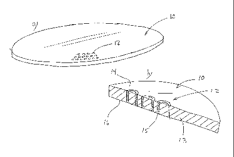
The invention in its broadest aspect is schematically illustrated in Figs. 1 a
and b (not to scale).
It comprises a wafer 10 of a conducting or a semi-conducting material, forming
a substrate
suitable for the manufacture of a large variety of micro-electronic devices,
an/or micro-
mechanic devices, and/or micro-optical devices, requiring components on both
sides of the
wafer, e.g. sensors, micro-mirror arrays, micro-optical components such as
lasers etc.
The inventive feature is the provision of vias 12, or electrical through
connections, extending
from a top side 14 of the wafer 10 to a bottom side 16. By means of the method
according to
the invention the vias comprise the same material as the material of the
wafer, i.e. they are
made from the wafer itself. Thus, no auxiliary material is used for the actual
electrical
connection.
In order to separate the vias 12 from the bulk 13 of the wafer in an
electrically insulating
manner, there is according to the invention oxide material 15 introduced
between the bulk 13
and the vias 12. The method will be described in further detail below.
By virtue of the fact that only "wafer native" material is used, i.e. the
material of the wafer
itself is used to manufacture the vias, the wafer having been provided with
said vias in a
desired structure, can be subjected to all the processing steps employed in
the semi-conductor
field, in terms of temperature, chemical environment, pressure etc, that a
"native wafer" can
be subjected to. Prior art devices (i.e. starting wafers for semiconductor
electronics
manufacture) comprising metallized portions, cannot be processed in the same
versatile way,
because the metallization will not withstand too high temperatures, or the
chemical agents
frequently used in etching and other procedures needed to make the desired
electronic or
micro-mechanic structures.
Another advantage is that the wafer according to the invention is flat
exhibiting a very low
surface roughness, down to mirror appearance.
CA 02519893 2005-09-19
WO 2004/084300 PCT/SE2004/000439
By "native wafer" and "native wafer material" we mean the material in the
original wafer
itself. "Auxiliary material" would therefore be any other material that has
been added to the
structure, such as a metal pad for connection purposes.
5 A "wafer" shall be taken to mean a general substrate usable as a starting
material for e.g.
MEMS applications. It is not necessarily completely flat, but can be provided
with predefined
structures such as depressions or other elements or members created by some
process
performed on the material from which the wafer is made.
In a first embodiment of the invention, illustrated in Fig. 2a - 2c (cross
sections of a wafer
during the different process steps; not to scale), the vias are made in a
process characterized
as comprising two general steps, namely provision of trenches and introducing
insulating
material into the grooves, and optionally filling the trenches, at least
partially with oxide.
The starting material is a conducting or a semiconductor wafer 20 (Fig. 2a),
suitably a silicon
wafer (although there are no specific limitations on the materials used),
having a thickness of
500 m, although the thickness can vary between 300 m and 1000 m. Most
commercially
available silicon (or other semi-conductor) wafers are about 300-1000 m thick,
depending on
size and intended application. However, the invention is applicable to wafers
exhibiting a
thicknes of 200 - 5000 gm, preferably 300 - 3000 gm, most preferably 400 -
1000 gm.
The first general step is the provision of a trench 21, i.e. a narrow recess
encircling a portion
of the wafer top surface. The trench is made for example by etching or by
laser based
machining, or by EDM (electro-discharge machining).
Trench definition is achieved by providing a lithographic mask 22 (Fig. 2b) on
the wafer,
which in itself does not form part of the invention. It is considered to
pertain to the field of the
skilled man to design and use suitable masking and etching techniques, given
the materials
used. Thus, a detailed discussion of the provision of the mask is not given
herein.
Preferably trenches are made by any etching method yielding a high aspect
ratio, e.g. DRIE
(Dry Reactive Ion Etching), electrochemical HF etch.
The trench should be less than 20 m, preferably 4-15, most suitably about 6-12
wide. Thus,
the layers of insulating material are 1-20 gm, typically 6-12 gm thick.
CA 02519893 2005-09-19
WO 2004/084300 PCT/SE2004/000439
6
If the wafer is 500 m thick, the trench is suitably about 200-490 m,
preferably 300-400 m
deep. Suitably the depth of the trench is about 50% up to 100% of the wafer
thickness. In the
case of 100% penetration, it is necessary that a thin oxide layer be present
on the surface, to
keep the formed "plug" in place.
With the method according to the invention, the pitch (center-to-center)
distance between the
electrical connections can be as small as 10 gm, typically 50-100 gm If there
is a thin oxide
layer provided on the bottom surface, the etch can be all the way through the
wafer until the
etch reaches the oxide, which acts as an etch stop. Thereby the via, i.e. the
cylindrical plug (in
the case of circular etch trench), will be supported by the oxide and
prevented from falling
out.
The shape of the portion encircled by the trench can be circular, but is of
course not limited
thereto. Any geometric shape that can be achieved is possible, such as
squares, rectangles,
triangles, romboids, traptezoids etc. or combinations of shapes (Fig. 3). The
only limitation
regarding the obtainable shapes is set by any inherent limitations of the
masking and etching
procedures employed.
Once the trench is made, the mask is removed, and the wafer is subjected to an
oxidizing
process in order to grow insulating oxide 24 in the trench (and on the
surfaces of the wafer
unless it is protected), Fig. 2c. This is achieved by increasing the
temperature to about 800-
1300 C, typically 1100 C, in an oxygen containing atmosphere. Optionally, the
oxidizing
process can be terminated before the trench is completely filled, and the
remaining space can
be filled with e.g. TEOS 26, in a deposition process, because of its good step
coverage
properties. However, any insulating material that is compatible with IC or
CMOS processing
conditions can be used. It is not even strictly necessary to fill the
trenches; it will suffice if the
material surrounded by the trench is kept at an insulating distance from the
wall. This can be
achieved by the very small bridging oxide portion at the bottom of the trench.
Frequently, when etching trenches having the high aspect ratio as in the
present invention, the
opening of the trench at the surface will be slightly narrower than the width
about 5-10 m
below the surface (See Fig. 2e). This phenomenon may cause the trench to
become
incompletely filled with oxide, thereby creating voids (air traps) which may
cause problems in
the further processing by IC, MEMS or CMOS techniques.
CA 02519893 2005-09-19
WO 2004/084300 PCT/SE2004/000439
7
In order to remedy this problem, suitably the wafer is subjected to a further
etch after the
trench defining mask work on the top surface of the wafer has been removed.
This etch will
thin down the surface slightly and remove the narrowing edges, leaving only a
strictly
"funnel" shaped trench cross section. The cross section after the etch is
indicate with broken
lines in Fig. 2e.
When the trench/trenches have been suitably filled with insulating oxide, to
the rate of filling
desired, the wafer, in a second step, is subjected to a thinning process.
Thereby, the back side
of the wafer is thinned down, by grinding or etching or other suitable method,
such that the
insulating oxide present in the trench/trenches becomes exposed on the back
side of the wafer
(indicated with a broken line in Fig. 2d). This procedure yields a plurality
of "plugs"
extending through the wafer and comprising a material which is identical to
the bulk material
of the wafer. The plugs will be surrounded by insulating oxide in patterns
defined by the
trenches. The surfaces of these plugs on the top and bottom of the wafer,
separated by the insu
lating oxide from the surrounding wafer material, represent bonding areas, to
which further
electronic elements can be bonded by suitable bonding techniques.
For certain applications it is necessary to provide cavities in a wafer,
wherein the bottom of
the cavity is provided with electrical connections. For such an application it
will be sufficient
to etch the surface selectively on those areas where said cavities are to be
formed. Thus, the
overall nominal thickness of the wafer can be maintained, and the etching to
expose the
insulating material, thereby creating the vias can be achieved only in said
depressions.
An example is the provision of deflectable micro-mirrors, where the deflection
is carried out
electrostatically by applying a voltage to an electrode in a cavity below the
deflectable mirror.
An embodiment of the invention for the above purpose will be described with
reference to
Figs. 12 and 13 below.
In a second embodiment of the invention, illustrated in Figs. 4a-b, the vias
are also made in a
process comprising two general steps, the first step of which is identical to
the first step of
first embodiment, thus yielding trenches 41 filled with insulating material
42, such as oxide
and optionally TEOS. Also in this embodiment, it might be sufficient to let
the oxide in the
bottom of the trench function as a spacer to keep the "plug" free from the
surrounding wall.
CA 02519893 2005-09-19
WO 2004/084300 PCT/SE2004/000439
8
This embodiment is primarily used when it is desirable to have a thicker
platform (wafer
substrate) 40 for the further manufacture. Since a trench can be made to
exhibit a depth of
about 400 m, it will be possible to make substrates comprising vias, and
having a thickness of
up to about 800 gm. However, if still thicker wafers, say up to 1000 m or
more are required,
the second etch from the bottom side, will generate wider trenches, since a
deep trench will
inevitably be wider at the opening than a shallow trench. Thus, in this
embodiment, the
thicker wafers will not be strictly symmetric in the sense that the vias will
not exhibit the
same appearance on both the top and bottom sides.
In the second step of the second embodiment, patterns 43 are defined by
lithographic methods
on the bottom surface, see Fig. 4a, said patterns matching the trenches
defined on the top
surface. This will require an alignment of the patterns. This is however not
part of the
invention per se, and alignment of patterns are considered to pertain to the
field of the skilled
man, and will not be further discussed herein.
Trenches are etched in the same way as the trenches on the top side (indicated
with a broken
line in Fig. 4a), until they meet the oxide in the trenches made in the first
step of the
procedure. The final structure is shown in Fig. 4b, wherein the vias are
designated 44, and the
insulating separating walls are designated 45.
In this embodiment a thinning of the wafer is avoided, but at the cost of
further processing
steps.
In a third embodiment (Figs. 5a - b), the first step of the method comprises
etching trenches
that extend all the way through the wafer. This means that the wafer 50 cannot
be thicker than
the maximum depth that is achievable by etching, i.e. about 400 m. However,
in this case, in
order that the vias will not fall out from the wafer, of course the trench
pattern must not define
closed structures. That is, each trench is represented by a "line" (see insert
in Fig. 5a), having
a beginning and an end, such as a semi-circle, or two legs of an angle. When
the first trench
52, extending through the wafer has been made, oxide is introduced into the
trench, possibly
the trench is filled with oxide. Then, a second trench 54, matching the first
so as to form a
closed structure, i.e. a second semi-circle matching the first semi-circle is
etched, and
subsequently filled with oxide, if desired.
CA 02519893 2005-09-19
WO 2004/084300 PCT/SE2004/000439
9
In principle the final shape can be achieved in several steps, which is still
within the inventive
concept, but for practical reasons a two-step procedure is the most
appropriate.
A further feature of the invention is to provide selectively doped vias, i.e.
the vias exhibit
higher conductivity than the bulk of the wafer. This can be achieved by
exposing the wafer
60, after trenches have been made, but before the mask work 61 is removed, to
a doping
process (see Fig. 6a). Doping material is thereby introduced (illustrated by
arrows) into the
trenches 62 (forming e.g. a circular shape), where it penetrates the walls in
the trench, and by
diffusion enters the material in the cylindrical plug and also in the wall
surrounding the plug
to a depth of up to about 15 m. A suitable exposure and annealing time will
yield a fully
doped, thus highly conductive via, whereas the bulk of the wafer is non-doped.
After
(optionally) filling the trenches with insulating material, the final
structure will be a wafer
comprising a plurality of high conductivity vias, insulated by means of an
oxide from the bulk
of the wafer which can be essentially non-conductive, except from a finite
region close to the
insulating material surrounding the vias. Due to the limited penetration
depth, vias up 30 m
in diameter can be made in the above indicated way. However, if a hole 63,
having a diameter
corresponding to the width of a trench, i.e. 5-10 m, is provided by etching
in the centre of
the area surrounded by the trench, the doping can be performed both from the
outer
circumferential trench and from the center hole. In this way the diameter of
the fully doped
via can be increased to about 60 m. In further embodiments it is possible to
provide a
plurality of concentric trenches, thereby enabling the provision of vias
exhibiting a diameter
as desired, theoretically exhibiting no limitations regarding size.
The vias resulting from the doping process is schematically illustrated in
Fig. 6b, wherein
dope regions are shown with denser hatching (the penetration depth of doping
in the bulk of
the wafer is shown with broken lines).
This feature will have utility in RF applications.
The invention will now be further illustrated by way of non-limiting examples.
EXAMPLES
Example 1 (prior art)
CA 02519893 2005-09-19
WO 2004/084300 PCT/SE2004/000439
In fig. 7 a prior art electrical connection structure is shown (corresponding
to Fig. 3 in US-
6,002,177). It comprises drilling holes in a silicon chip and metallizing the
internal walls of
said holes to provide electrical connections between the two sides of the
chip.
5 Example 2 (demonstration of problem with standard trench etch)
A standard trench etch was performed on a silicon wafer. The wafer was 100 mm
in diameter
and 500gin thick.
10 In order to provide the trenches, a patterned mask was provided on one
surface (top surface)
of the wafer, by standard lithographic technique. The trenches in this example
were simple
"line" shaped trenches.
The etching process was a so called DRIE (Deep Reactive Ion Etch)
A series of trenches exhibiting varying depth and width was made the depths
varying between
200 and 400 m and the width between 5 and 12 gm. In Fig. 8 a magnified view of
the top
opening of a trench is shown. As can be clearly seen, the opening is narrower
than the trench
about 10 gm down in the trench. This phenomenon causes frequently an
incomplete filling of
the trench in a subsequent oxide filling step.
Example 3 (elimination of the standard etch drawback)
Therefore, in order to remedy this problem, an additional, shallow etch as
described in
connection with Fig. 2e was performed.
This process step yields a strictly monotonic trench shape, as can be seen in
Fig 9a, i.e. the
opening is the widest part of the trench, which than gradually becomes
narrower. Fig. 9b
shows the structure of a plurality of trenches after the shallow etch.
Filling this trench structure with oxide, will result in a completely filled
trench with no voids.
Example 4
In Fig. 10 an example of an array of completed vias having a rectangular shape
is shown.
CA 02519893 2005-09-19
WO 2004/084300 PCT/SE2004/000439
11
Example 5
Fig. 11 shows an array of vias made according to the embodiment where etching
from both
sides of the wafer has been employed.
Example 6
In Fig. 12 there is shown a schematic process sequence for making a MEMS
device, in
particular an array of deflectable micro mirrors.
The starting substrate is an ordinary silicon wafer 70, Fig. 12a. Trenches72
are etched to a
certain depth, as described above, and filled with oxide 74, see Fig. 12b.
Then, a local area on
the opposite side of the wafer (with respect to the trenches) is etched to
provide a depression
75 (or cavity), reaching down to where the trenches end, whereby the insulated
(preferably
circular cylindrical through connections) are exposed, see Fig. 12c. A
membrane or an array
of micro-mirrors, or some other suitable element or member (schematically
indicated with
reference numeral 76 in Fig. 12c), as desired, is provided over the cavity,
and the electrical
through connections can be used for actuating e.g. a deflectable
membrane/mirror by applying
a suitable voltage. This can suitably be achieved by providing solder bumps 78
for flip-chip
mounting or metal pads for wire bonding, to provide connection to some power
source or
other energizing device. Technology for manufacturing SLM's (Spatial Light
Modulators)whereby the present invention can be used, is disclosed in our
pending US patent
application serial no. 10/654,007.
Example 7
In Fig. 13 a further embodiment of a process sequence for making a MEMS device
is
schematically illustrated.
Thereby the starting material is a SOI wafer (Silicon On Insulator) 80,
wherein an oxide layer
82is buried inside a silicon wafer, Fig. 13a. Trenches 84 are etched and
filled with oxide 86,
as described above, but due to the presence of the oxide layer, the trenches
will only reach
exactly down to the oxide layer, which acts as an etch stop, Fig 13b. This is
an advantage over
the embodiment of Fig. 12, wherein the bottoms of each trench may be located
at slightly
CA 02519893 2005-09-19
WO 2004/084300 PCT/SE2004/000439
12
different depths, such that when a depression is etched from the opposite side
of the wafer, the
through connections may extend slightly above the bottom surface of the
depression. This is
schematically illustrated in Fig. 12c, wherein it can be seen that there is a
slight variation in
how much each trench protrudes above the cavity bottom.
On the contrary, in the embodiment of Fig. 13, when the depression 88 is made
by etching,
first the buried oxide layer 82 will be reached, and then, when the oxide
layer is removed, the
trenches will be located exactly at the same level inside the depression, see
Fig. 13c, or
essentially "flush" with the bottom surface of said depressions. In fact, the
trenches can be
"over etched" to ensure that all the trenches reach the same depth.
Thus, by the disclosure and examples given above, it has been shown that with
the present
invention, there is provided a product in the form of a starting substrate, in
the form of a
conducting or semi-conducting wafer, that can be used for the purposes of
manufacturing a
large variety of semi-conductor devices. By virtue of the wafer already from
the start
comprising electrical connections extending through the wafer (vias), it will
become possible
to design and make structures on both sides of the wafer in a very versatile
way. The fact that
the vias are made form the original wafer itself, makes the wafer capable of
withstanding all
process conditions usable with plain silicon wafers.