Note : Les descriptions sont présentées dans la langue officielle dans laquelle elles ont été soumises.
CA 02520824 2005-09-26
SPECIFICATION
SELF LIGHT - EMITTING DEVICE
TECHNICAL FIELD
The present invention relates to a self light-emitting device that allows
one or more luminous bodies to emit light using electric power generated by a
photo-electric converting element.
BACKGROUND OF THE RELATED ART
Conventionally, various self light-emitting devices, which allow one or more
luminous bodies to emit light using electric power generated by a photo-
electric
converting element, such as a solar battery, have been proposed. For example,
in
the publication of Japanese Laid-Open Patent Application Hei 9 - 49213, a road
installation type signaling device equipped with a flat solar battery,
multiple light
emitting diodes arranged around the solar battery and a storage cell where
electric power generated by the solar battery is accumulated is proposed. In
this
signaling device, the entire device is buried and installed in the road, and
the
electric power generated by the solar battery is accumulated in the storage
cell
during the day, and the light emitting diodes blink due to the electric power
accumulated in the storage cell during the night.
In Japanese Laid-Open Patent Application Hei 8 - 199513, a light emitting
indicator equipped with a flat solar battery, plural light emitting diodes, a
storage
cell and an electric circuit, and in which these constructional elements are
buried
1
CA 02520824 2005-09-26
into transparent epoxy resin, is proposed. Even in this light emitting
indicator,
the electric power generated by the solar battery is accumulated in the
storage
cell during the day, and the light emitting diodes blinks using the electric
power
during the night. Burying the construction elements into the epoxy resin
results
in improved weather resistance.
However, in the devices described in Japanese Laid-Open Patent Application
Hei 9 - 49213 and Japanese Laid-Open Patent Application Hei 8 - 199513, since
electric power is generated by a flat solar battery, high power electricity
cannot be
always generated during the day, but the high power electricity can be
generated
only for several hours when the sunlight enters almost vertically into the
solar
battery at a small angle of incidence. In other words, since the electric
power
required at night has to be accumulated during several hours, the light
receiving
area of the solar battery has to be large, with the problem that the device
becomes
excessively large.
When installing the devices described in Japanese Laid-Open Patent
Application Hei 9 - 49213 and Japanese Laid-Open Patent Application Hei 8 -
199513 on a flat road, electric power can be accumulated in the storage cell.
However, if the devices are installed on a slope, such as a slope formed on an
inclined plane on the north side, since a great deal of sunlight is reflected
on the
surface of the solar battery, the desired electric power cannot be accumulated
in
the storage cell and the light emitting diodes cannot emit light during the
night,
making it difficult for drivers in vehicles traveling on the road to drive
safely.
In recent years, a low cost, small and light weight self light-emitting
device used for the purpose of safety at night by attaching it to a bicycle, a
bag or a
cap has been desired. When attaching these devices, a self light-emitting
device
2
CA 02520824 2009-12-15
is often installed close to a vertical state, and the electric power, which is
supposed to
accumulate in the storage cell cannot be generated because the sunlight enters
almostparallel
to the acceptance surface, making it impossible to practically use.
The objective of the present invention is to provide a self light-emitting
device,
where electric power to be generated is not affected by the installation
location, and which
can be manufactured at a low cost and is small and light weight.
SUMMARY OF THE INVENTION
A light-emitting device according to one aspect of the invention comprises:
spherical
photo-electric converting elements connected in series and each having a
substantially
spherical light receiving surface; a condenser for accumulating electric power
generated by
said spherical photo-electric converting elements; luminous bodies for
emitting light and
powered by said photo-electric converting elements; a light emitting control
circuit for
controlling a conduction of electric power to said luminous bodies; a photo-
detecting sensor
incorporated into said light emitting control circuit, said photo-detecting
sensor having a
light sensor and an amplifying circuit to amplify an output of the light
sensor to reflect an
intensity of light rays detected by said light sensor and transmit the
amplified output in said
light emitting control circuit; said light emitting control circuit
selectively driving said
luminous bodies to emit light based upon the amplified output of said light
sensor; and
a sealing member for enclosing the light emitting device into an integral
unit. The light-
emitting device may comprise a reflection member formed from a transparent
resin material
having a reflective surface that is provided adjacent to said spherical photo-
electric
converting elements and said luminous bodies, and the light sensor may be an
ultraviolet
light sensor. Preferably, the light-emitting device may comprises a lens
member for guiding
or condensing light to said spherical photo-electric converting element.
In this self light-emitting device, when incidental light enters into the self
light-
emitting device, the incidental light is guided or condensed by the lens
member; the
incidental light is received on the substantially spherical light receiving
surface of the
3
CA 02520824 2009-12-15
spherical photo-electric converting element, electric power is generated; and
the luminous
body emits light using the electric power. In this self light-emitting device,
since the light
receiving surface of the spherical photo-electric converting element is formed
to be
substantially spherical, electric power can be generated on average as long as
incidental light
enters without depending upon the angle of the incidental light. Therefore,
with an outside
installation, electric power can be generated on average during the day
regardless of the
angle of incidence of the sunlight. in addition, when constructed to
accumulate the
generated electricity in a storage cell, sufficient electric power can be
accumulated in the
storage cell during the day regardless of the position of sun for several
house as long as the
weather is fine.
Another aspect of the invention provides a light-emitting device, comprising
spherical photo-electric converting elements connected in series and each
having a
substantially spherical light receiving surface; a lens member for guiding or
condensing light
to said spherical photo-electric converting element; a condenser for
accumulating electric
power generated by said spherical photo-electric converting elements; luminous
bodies for
emitting light and powered by said photo-electric converting elements; a light
emitting
control circuit for controlling a conduction of electric power to said
luminous bodies; a
photo-detecting sensor incorporated into said light emitting control circuit,
said photo-
detecting sensor having an ultraviolet sensor and a direct-current amplifying
circuit for
amplifying a voltage corresponding to an intensity of ultraviolet rays
detected by said
ultraviolet sensor and for transmitting the amplified voltage in said light
emitting control
circuit, and said light emitting control circuit selectively driving said
luminous bodies to emit
light based upon the amplified voltage as an output of said ultraviolet
sensor; and a scaling
member for enclosing the light emitting device into an integral unit, The lens
member and
said sealing member may be formed with the same type of synthetic resin
material. The
device may further comprise a reflection member that is formed from a
transparent resin
material having a reflective surface that is provided adjacent to said
spherical photo-electric
4
CA 02520824 2009-12-15
converting elements and said luminous bodies. The light emitting control
circuit may
selectively drives one of said luminous bodies at a time to emit light based
upon the output
of said ultraviolet sensor so as to indicate a range of the intensity of
ultraviolet rays detected
by said ultraviolet sensor.
Yet another aspect of the invention provides light emitting device comprising:
spherical photo-electric converting elements each comprising: a spherical
crystal formed of
one of p type semiconductor and n type semiconductor material; a diffusion
layer formed
adjacent a surface ofthe spherical crystal; a pn junction formed by said
diffusion layer in the
spherical crystal; first and second electrodes connected to opposing sides of
the pnjunction
and respectively disposed on opposing top and bottom sides of said spherical
crystal with a
center of said spherical crystal disposed substantially between the first and
second
electrodes; and a substantially spherical light receiving surface;
semispherical lens members
for directing light to the spherical photo-electric converting elements;
partial-spherical
metallic reflection members disposed below the spherical photo-electric
converting elements
and configured to reflect light incident on the partial-spherical metallic
reflection members
to a lower surface of said spherical photo-electric converting elements, each
of said partial-
spherical metallic reflection members being configured to function as a lead
frame and being
connected to the second electrode of a corresponding one of said spherical
photo-electric
converting elements disposed above said partial-spherical metallic reflection
member; a
luminous device for emitting light using power from said spherical photo-
electric converting
elements; a synthetic resin member integrally formed with the lens members and
embedding
the spherical photo-electric converting elements, the luminous device, and the
partial-
spherical metallic reflection members; and said spherical photo-electric
converting elements
being connected in series by said first electrodes of each of said spherical
photo-electric
converting elements, with exception of a last one of said spherical photo-
electric converting
elements in the series, being connected to one of the partial-spherical
metallic reflection
4A
CA 02520824 2009-12-15
members disposed below an adjacent one of said spherical photo-electric
converting
elements in the series.
The second electrodes maybe connected to the partial-spherical metallic
reflection
members by a conductive bonding material. The luminous device may have a first
electrode
bonded to by conductive material to an extension of one of said partial-
spherical metallic
reflection members corresponding to said last one of said spherical photo-
electric converting
elements in the series, and said luminous device has a second electrode
electrically
connected to a first electrode of a first one of said spherical photo-electric
converting
elements in the series.
Even when attaching the device to a bicycle, a bag or a cap, sufficient
electric power
can be always generated without being affected by the attached angle, so a
luminous body
can emit the light- Since incidental light is guided or condensed by the lens
member, even
if the light receiving area of the spherical photo-electric converting element
is small, strong
incidental light is received on the light receiving surface, so
miniaturization and light weight
of the photo-electric converting element can be realized. On the same time,
the
miniaturization and light weight of the self light-emitting device can be
realized. Since the
entire device is embedded integrally in the scaling member, any damage of the
spherical
photo-electric converting element or the luminous body due to rain can be
prevented.
Further, since inexpensive material can be used for each constitutional
element, production
cost can be reduced.
Herein, the following constitution may be appropriately adopted:
1) As the photo-electric converting element, multiple series-connected
spherical
photo-electric converting elements are applicable.
2) A condenser for accumulating electric power generated by the spherical
photo-
electric converting element is provided.
3) A light emitting control circuit for controlling a conduction of electric
power to
the luminous body is provided.
4) A photo-detecting sensor is incorporated into the light emitting control
circuit.
4E
CA 02520824 2005-09-26
5) The light emitting control circuit comprises an astable multivibrator
including two transistors and multiple resistances.
6) A charge control circuit for controling charging to the condenser is
provided.
7) The lens member and the sealing member are formed with the same
type of synthetic resin material.
8) A partial spherical metallic reflection member for reflecting incident
light to the lower surface side of each of the spherical photo-electric
converting
elements.
9) The reflection member may be made from a lead frame.
10) The photo-detecting sensor is made from an ultraviolet sensor, and a
direct-current amplifying circuit to amplify a voltage according to the
intensity of
ultraviolet rays detected by the ultraviolet sensor and transmits the
amplified
voltage, and is provided in the light emitting control circuit.
11) A plurality of luminous bodies are provided, and the light emitting
control circuit allows any of the luminous bodies to emit light based on the
output
from the ultraviolet sensor.
12) A schmitt trigger inverter and resistors are incorporated in the light
emitting control circuit in parallel for making the luminous body blink.
13) The condenser is a manganese dioxide-lithium secondary battery.
14) A reflection member formed with a light reflectible transparent resin is
provided adjacent to the spherical photo-electric converting elements and the
luminous body.
15) The photo-detecting sensor is formed with cadmium sulfide (CdS).
5
CA 02520824 2005-09-26
BRIEF DESCRIPTION OF THE DRAWINGS
Fig. 1 is a plane view of the self light-emitting device of the first
embodiment of the present invention.
Fig. 2 is a cross-sectional view along II-II line in Fig. 1.
Fig. 3 is a cross-sectional view of a spherical photo-electric converting
element.
Fig. 4 is a block diagram for explaining a control system of the self
light-emitting device.
Fig. 5 is a circuit diagram for explaining a light emitting control circuit.
Fig. 6 is a circuit diagram for explaining a charge control circuit.
Fig. 7 is a circuit diagram of a light emitting control circuit relating to a
modified embodiment.
Fig. 8 is a cross-sectional view of a spherical photo-electric converting
element relating to a modified embodiment.
Fig. 9 is a plane view of a self light-emitting device of the second
embodiment.
Fig. 10 is a cross-sectional view along X-X line in Fig. 9.
Fig. 11 is a plane view of a panel-type self light-emitting device.
Fig. 12 is a cross-sectional view along XII-XII line in Fig. 11.
Fig. 13 is a plane view of an ultraviolet monitoring device of the third
embodiment.
Fig. 14 is a cross-sectional view along XIV-XIV line in Fig. 13.
Fig. 15 is a circuit diagram of a light emitting control circuit of the
ultraviolet monitoring device in Fig. 13.
Fig. 16 is a perspective view of a self light-emitting cube of the forth
6
CA 02520824 2005-09-26
embodiment.
Fig. 17 is a plane view of the self light-emitting name plane of the fifth
embodiment.
Fig. 18 is a cross-sectional view of the self light-emitting name plate
shown in Fig. 17.
Fig. 19 is a circuit diagram of a light emitting control circuit of the self
light-emitting name plate shown in Fig. 17.
Fig. 20 is a plane view of a four-color self light-emitting device of the
sixth
embodiment.
Fig. 21 is a cross-sectional view along XXI-XXI line in Fig. 20.
Fig. 22 is a circuit diagram of the self light-emitting control circuit of the
four-color self light-emitting device shown in Fig. 20.
Fig. 23 is a plane view of a self light-emitting pendant of the seventh
embodiment.
Fig. 24 is a cross-sectional view along XXIV-XXIV line in Fig. 23.
DETAILED DESCRIPTION OF PREFERRED EMBODIMENTS
Embodiment 1 (refer to Fig. 1 through Fig. 7)
Embodiment 1 of the present invention are described hereafter, with
reference to the drawings. The present embodiment is an example where the
present invention is applied to a mobile self light-emitting device, where a
light
emitting diode blinks only in the state where light is low, such as at night.
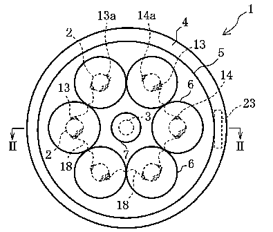
As shown in Fig. 1 and Fig. 2, a self light-emitting device 1 is equipped
with six spherical photo-electric converting elements 2, a light emitting
diode 3, a
sealing member 4 and a control circuit 5.
7
CA 02520824 2005-09-26
The spherical photo-electric converting elements 2 are similar to those
described in detail in Japanese Laid-Open Patent Application 2001 - 168369,
and
is briefly described here. As shown in Fig. 3, the spherical photo-electric
converting element 2 is equipped with a spherical crystal 10 made from a p-
type
silicon semiconductor, the diameter of which is approximately 1.5 mm and
resistivity is approximately 1 Q cm; an n-type diffusion layer 12 formed in
the
vicinity of the surface of the spherical crystal 10 for the purpose of forming
a
substantially spherical pn-joint 11; a positive electrode 13 electrically
connected to
the p-type silicon of the spherical crystal 10; a negative electrode 14 formed
at a
position point- symmetrically facing the positive electrode 13 relative to the
center
of the spherical crystal 10, and electrically connected to the n-type
diffusion layer
12; and an insulation film 15 formed on the surface of the spherical crystal
10 at
sections where the electrodes 13, 14 are not formed. In addition, an Al paste
film
16 with approximately 20 gm of thickness is coated on the surface of the
positive
electrode 13, and an Ag paste film 17 with approximately 20 m of thickness is
coated on the surface of the negative electrode 14. When light, such as
sunlight,
enters into the spherical photo-electric converting elements 2, the incidental
light
transmits through the n-type diffusion layer 12 and enters the pn-joint 11,
and a
photo-electromotive force is generated on the pn-joint 11. The
photo-electromotive force of these spherical photo-electric converting
elements 2 is
approximately 0.6 V, and approximately 3 - 3.5 mA of electric current can be
discharged.
As shown in Figs. 1 and 2, six spherical photo-electric converting elements
2 are arranged around the light emitting diode 3 at approximately 60 of
intervals. The positive electrode 13 of each spherical photo-electric
converting
8
CA 02520824 2005-09-26
element 2 is electrically connected to the negative electrode 14 of the
adjacent
spherical photo-electric converting element 2 by a copper line 18,
respectively, and
the six spherical photo-electric converting elements 2 are connected with each
other in series. However, a positive electrode 13a and a negative electrode
14a,
equivalent to both ends of the series connection among the positive electrodes
13
and the negative electrodes 14 in the six photo-electric converting elements
2, are
connected to the control circuit 5 to accumulate the generated electric power.
The light emitting diode 3 has an AlGaAs-based hetero structure, and as
shown in Fig. 1, is arranged substantially in the center of the self light-
emitting
device 1. This light emitting diode 3 blinks only where light is low, such as
at
night, by the below-mentioned light emitting control circuit 22 using the
electric
power generated by the spherical photo-electric converting elements 2 and
accumulated in a condenser 21.
The sealing member 4 is formed with appropriate synthetic resin, such as
epoxy resin, and embeds integrally the whole elements such as the spherical
photo-electric converting elements 2, the light emitting diode 3 and the
control
circuit 5. Condenser lenses 6 to guide or condense incident light are
integrally
formed in a position corresponding to the external surface side of each
spherical
photo-electric converting element 2, respectively, and a projection lens 7 is
also
integrally formed at a position corresponding to the light emitting diode 3,
on the
upper surface of the sealing member 4. As shown in Fig. 2, the surfaces of the
condenser lenses 6 are formed to be hemispheric, regarding the spherical
photo-electric converting element 2 as a center, respectively, and light
entering
the surfaces of the condenser lens 6 is condensed to the spherical photo-
electric
converting element 2, respectively. The surface of the projection lens 7 is
formed
9
CA 02520824 2005-09-26
to be partially spheroidal, and light emitted from the light emitting diode 3
is
diffused by the project lens 7 and transmitted to the outside. Furthermore,
the
epoxy resin that forms the sealing member 4 including the lenses 6 and 7 is a
material capable of transmitting a photo- electrically converted light by the
spherical photo-electric converting elements 2.
The control system of this self light-emitting device 1 is described next.
As shown in Fig. 4, the control circuit 5 is equipped with a charge control
circuit 20, a condenser 21 made of a capacitor, and a light emitting control
circuit
22. These charge control circuit 20, condenser 21 and light emitting control
circuit 22 are mounted on the same substrate, and as shown in Fig. 2, are
arranged on the lower sides of the spherical photo-electric converting
elements 2
and the light emitting diode 3. The control circuit 5, in a state in which
electric
power is generated by the spherical photo-electric converting elements 2
during
the day, the light emitting control circuit 22 prohibits the light emitting
diode 3
from emitting light, and the generated electric power is charged in the
condenser
21 by the charge control circuit 20; and in a state in which light is low,
such as at
night, the light emitting diode 3 is driven to emit blinking light by the
light
emitting control circuit 22 using the electric power accumulated in the
condenser
21.
The charge control circuit 20 is for the control of the charge to the
condenser
21; to prevent excess current to the condenser 21; and to prevent reverse
current
to the spherical photo-electric converting elements 2. As shown in Fig. 6, the
charge control circuit 20 comprises a diode D to prevent reverse current and a
constant-voltage element ZD.
The operation of the charge control circuit 20 is described next.
CA 02520824 2005-09-26
The electric current generated by electric power generating device 2A where
the six spherical photo-electric converting elements 2 are connected in series
is
charged in the condenser 21 via the diode D. If incidental light to the
electric
power generating device 2A decreases and the output voltage of the condenser
21
is greater than that of the spherical photo-electric converting elements 2,
the
diode D functions to prevent reverse current from the condenser 21 from
reaching
the electric power generating device 2A. When the electric power accumulated
in
the condenser 21 reaches a pre-determined voltage, the constant-voltage
element
ZD grounds the electric power generated by the electric power generating
device
2A, preventing excess current from reaching the condenser 21 and enables the
prolongation of the life of the condenser 21. Furthermore, if the maximum
output of the electric power generating device 2A is smaller than the sum of
the
maximum allowable voltage and the threshold voltage of the diode D, the
constant-voltage element ZD can be omitted. The light emitting control circuit
22 controls the power distribution to the light emitting diode 3 and for
blinking
the light emitting diode 3 in a state in which light is low, such as at night.
As
shown in Fig. 5, the light emitting control circuit 22 is a control circuit
where a
photo-detecting sensor 23 is incorporated into the astable multivibrator,
which
has two transistors Q1, Q2, four resistors R1, R2, R3, R4 and condensers C1,
C2.
The photo-detecting sensor 23 is an optical response resistive element mainly
formed with CdS, and its resistance value changes depending upon the quantity
of
a received light. Furthermore, the resistance values of each resistor are, for
example, R1= 3.3 Q, R2 = 1 MQ, R3 = 510 kQ and R4 = 51 kS2.
The operation of this light emitting control circuit 22 is described next.
First, an operation in a state in which light has been detected by the
11
CA 02520824 2005-09-26
photo-detecting sensor 23, such as during the day, is described. In a state in
which the light has been detected by the photo-detecting sensor 23, because
the
resistance value for the photo-detecting sensor 23 decreases and the base of
the
transistor Q1 is grounded, the base electrical potential of the transistor Q1
decreases to a threshold or less, and no conduction between a collector and
emitter
of the transistor Q1 occurs and no electric current flows to the resistor R1.
In the
meantime, the base electric potential of the transistor Q2 becomes a threshold
or
greater, so electric current flows from the resistor R4 to the earth. However,
due
to 51 kQ of resistance value on the resistor R4 and the maximum voltage 3V
applied to the resistor R4, the maximum electric current flowing into the
resistor
R4 is only several dozens A. In the meantime, because the electric current
flowing from the electric power generating device 2A to the condenser 21 is
several
mA, charging the condenser 21 is hardly affected.
An operation where the light emitting diode 3 is driven to blink by the
light emitting control circuit 22 when no light is detected by the photo-
detecting
sensor 23, such as at night, is described next.
In a state in which light is low, such as at night, if no light is detected by
the photo-detecting sensor, the resistance value for the photo-detecting
sensor 23
increases and the base electric potential of the transistor Q1 gradually
ascends.
Accompanying the ascent of the base electric potential of the transistor Q1,
electric current flowing in the resistor R2 flows via the condenser C2, so
electrical
charge is accumulated in the condenser C2.
When the base electric potential of the transistor Qi reaches the threshold,
the cut-off state between the collector and the emitter of the transistor Q1
instantaneously changes to the conduction state. In a state in which light is
12
CA 02520824 2005-09-26
detected by the photo-detecting sensor 23, positive electric charge is
accumulated
in the electrode of the condenser C1 on the resistor R1 side, and negative
electric
charge is accumulated in the electrode of the condenser C1 on the resistor R3
side.
Because conduction between the collector and the emitter of the transistor Ql
causes the instantaneous descent of the electric potential at a junction point
P1 of
the light emitting diode 3, the resistor R1 and the condenser C1, and the base
electric potential of the transistor Q2 becomes a threshold or less due to the
electric charge accumulated in the condenser C1, and the transistor Q2 is
blocked.
In the meantime, the conduction of the transistor Q1 causes the flow of the
electric current via a route of the light emitting diode 3, the resistor Rl
and
between the collector and the emitter of the transistor Q1; and the light
emitting
diode 3 emits light. Because the electric current flows into the condenser C1
via
the resistor R3, only a pre-determined quantity of the electric charge
accumulated
in the condenser C1 is discharged. After the electric charge is discharged due
to
the electric current flowing via the resistor R4, the electric charge is
accumulated
in the condenser C2.
Since the condenser C1 is gradually charged due to the electric current
flowing into the resistor R3, the base electric potential of the transistor Q2
gradually ascends. When the base electric potential of the transistor Q2
reaches
the threshold, the cut-off state between the collector and the emitter of the
transistor Q2 instantaneously changes to the conduction state. When the
conduction of the transistor Q2 causes grounding of the collector of the
transistor
Q2, the base electric potential of the transistor Q1 instantaneously descends
to
the threshold or less due to the electric charges accumulated in the condenser
C2,
and conduction between the collector and the emitter of the transistor Q1
13
CA 02520824 2005-09-26
instantaneously changes to the cut-off state.
When the transistor Q2 is conducted, the electric current flows via the
route of the light emitting diode 3, the condenser C1 and between the base and
the
emitter of the transistor Q2, and via a route of the resistor R3 and between
the
base and the emitter of the transistor Q2. When the condenser C1 is charged to
a
pre-determined quantity due to the electric current flowing via the light
emitting
diode 3, no electric current flows into the light emitting diode 3 and the
light
electric diode 3 turns the light out. The accumulated electric charge is
gradually
discharged into the condenser C2 due to the electric current flowing via the
resistor R2, and the condenser C2 is charged. As the condenser C2 is charged,
the base electric potential of the transistor Q1 gradually ascends, and when
it
reaches a threshold, the transistor Q1 conducts. In the meantime, the
transistor
Q2 is cut off and the light emitting diode 3 emits light again. Subsequently,
the
operation is repeated, and the light emitting diode 3 is driven to blink.
Compared to the internal resistance of the light emitting diode 3 and the
resistance value of the resistor R4, which are the charging route of the
condenser
C1 and the condenser C2, the resistance values for the resistor R3 and the
resistor
R2 are established to be sufficiently great, so the interval time to blink the
light
emitting diode 3 is determined according to the discharge time C1 and C2,
respectively. In other words, the time to emit light and to turn the light off
depends upon (the electric capacity of the condenser Ci) x (the resistance
value of
the resistor R3) and (the electric capacity of the condenser C2) x (the
resistance
value of the resistor R2).
The test results are described next. When using the self light-emitting
device 1 where a capacitor with 2F of electrostatic capacity is applied as the
14
CA 02520824 2005-09-26
condenser 21, when the sample is charged under the 100,000 lx of illuminance
within a solar simulator, electric power is accumulated in the condenser 21 in
1
hour, and it is possible that the light emitting diode 3 emits blinking light
for 8
hours or longer with a light emitting pattern of 1 - 3 mcd of emission
luminance
and 30 % of duty ratio. Furthermore, this self light-emitting device 1 is
configured with approximately 20 mm of diameter, approximately 3 mm of
thickness according to a planar view, and approximately 5g of weight. When
using the self light-emitting device 1 where a capacitor with 0.47 F of
electrostatic
capacity is applied as the condenser 21, when the sample is charged under
100,000 lx of illuminance within a solar simulator, the electric power is
accumulated in the condenser 21 in 20 min., and it is possible that the light
emitting diode 3 emits blinking light for 2 hours or longer with a light
emitting
pattern of 1- 3 mcd of emission luminance and 30 % of duty ratio. Furthermore,
the self light-emitting device 1 with this construction is configured with
approximately 12 mm of diameter and approximately 3 mm of thickness according
to a planar view, and approximately 3 g of weight.
An operation and the efficacy of the self light-emitting device 1 is
described next. With this self light-emitting device 1, since the light
receiving
surface (pn-joint 11) of the spherical photo-electric converting elements 2
that
generate electric power is formed to be substantially spherical, respectively,
when
the present embodiment, it is possible to generate electric power relative to
incidental light at any angle from the upper side, and electric power can be
generated regardless of the installation location or installation angle and
the
generated electric power can accumulate in the condenser 21, improving the
degree of freedom for the installation location and the installation angle.
The
CA 02520824 2005-09-26
establishment of the six spherical photo-electric converting elements 2
enhances
the power generation voltage to be 6 times greater compared to when generating
electric power by one spherical photo-electric converting element 2, realizing
a
reduction of charging time. Since the condenser lenses 6 are formed, incident
light can be condensed and received on the spherical photo-electric converting
elements 2, so the introduction efficiency of light, such as sunlight, can be
improved. As described above, since it is possible to blink the light emitting
diode 3 for 8 hours with 1 hour of accumulation of electric power, even though
the
weather may be somewhat bad, the situation where the light emitting diode 3
will
no longer emit light can be prevented.
The self light-emitting device 1 can greatly realize the described
miniaturization and light weight, so it can be easily carried, and even if it
is
attached to a bag or a cap, the user hardly feels a burden. The sealing member
4
including the lenses 6, 7 embeds integrally the whole elements such as the
spherical photo-electric converting elements 2, the light emitting diode 3 and
the
control circuit 5, so the self light-emitting device 1 is resistant to rain
and dust,
with excellent weather resistance, and it can be installed at any location,
and even
if it is carried, it will not become damaged. Forming the lenses 6, 7 with
epoxy
resin, which is the same as the sealing member 4, enables additional
improvement of strength.
Since the self light-emitting device 1 is equipped with the condenser 21,
the light emitting diode 3 can emit light even in a state in which it is
impossible to
generate electric power by the spherical photo-electric converting elements 2,
such
as at night. The application of an astable multivibrator to the light emitting
control circuit 22 enables blinking the light emitting diode 3, with improved
16
CA 02520824 2005-09-26
surrounding visibility. Since the photo-detecting sensor 23 is incorporated in
the
position shown in Fig. 5, the grounded electric current from the condenser 21
can
be controlled to be minimal, shortening the charging time, and, and emission
from
the light emitting diode 3 can be prohibited. Since the self light-emitting
device
1 is equipped with the charge control circuit 20 shown in Fig. 6, any excess
current to the condenser 21 can be prevented, and any reverse current to the
spherical photo-electric converting elements 2 from the condenser 21 can also
be
prevented, prolonging the life of the condenser 21 and the spherical photo-
electric
converting elements 2.
A modified embodiment of the light emitting control circuit 22 is described
next. The astable multivibrator using transistors is applied to the light
emitting
control circuit 22. However, as shown in Fig. 7, a light emitting control
circuit
22A that has an astable multivibrator using IC can be applied. Furthermore,
the
same ones as those of the embodiment are applied to the photo-detecting sensor
23, the light emitting diode 3 and the condenser 21, respectively, so the same
reference numerals are used and the description is omitted.
An operation of the light emitting control circuit 22A is described next.
Since the light emitting control circuit 22 is a control circuit where the
photo-detecting sensor 23 is applied to a general IC type astable
multivibrator 25,
it is briefly described. In a state in which light is detected by the photo-
detecting
sensor 23, such as during the day, electric current discharged from the
condenser
21 is grounded via the resistor R5 and the photo-detecting sensor 23, an input
terminal 12 of an NAND circuit ND4 is always maintained at a low level, so the
output of the NAND circuit ND4 becomes a high level. Therefore, since electric
current will not flow into the light emitting diode 3, the light emitting
diode 3 will
17
CA 02520824 2005-09-26
not emit light. However, since a resistor with a very great resistance value
is
applied to the resistor R5, even if light is detected by the photo-detecting
sensor
23, electric current discharged from the condenser 21 via the resistor R5 is
small,
so charging the condenser will hardly be affected.
Operation of the light emitting control circuit 22A is described in a state
in which light is hardly detected by the photo-detecting sensor 23, such as at
night,
so the resistance value for the photo-detecting sensor 23 becomes greater and
electric current hardly flows into the photo detecting sensor 23. Since
electric
current hardly flows into the photo-detecting sensor 23 in this state, the
input
terminal 12 of the NAND circuit ND4 is always at a high level. If the input
side
of an NAND circuit ND1 is initially at a low level and no electric charge has
been
accumulated in the condenser C4, since the output side of the NAND circuit ND1
is at a high level, electric current flows to the output of the NAND circuit
ND 1,
the condenser C4, a resistor R7, a diode D2 and the output of an NAND circuit
ND2, and electric charge is accumulated in the condenser C4.
The condition where the electric charge has started being accumulated in
the condenser C4 is the same condition where the condenser C4 is short-
circuited,
so the input of the NAND circuit ND2 becomes a high level. As a result, the
output of the NAND circuit ND2 is at a low level. In this state, the input of
the
NAND circuit ND3 becomes a low level and the output becomes a high level, so
the input terminal 11 of the NAND circuit ND4 also becomes a high level. As a
result, because the input terminal 12 of the NAND circuit ND4 is also at a
high
level, the output of the NAND circuit ND4 becomes a low level, and electric
current flows into the light emitting diode 3 from the condenser 21, and the
light
emitting diode 3 emits light.
18
CA 02520824 2005-09-26
Next, when the electric charge is accumulated in the condenser C4, the
electric current flowing into the condenser C4 diminishes, and the voltage on
the
input side of the NAND circuit ND2 gradually descends, and when the voltage on
the input side of the NAND ND2 becomes a threshold voltage, the input of the
NAND circuit ND2 instantaneously becomes a low level. Associated with this,
the output becomes a high level. When the output of the NAND circuit ND2
becomes a high level, the input of the NAND circuit ND3 becomes a high level
and
the output becomes a low level. Then, the input terminal 11 of the NAND
circuit
ND4 becomes a low level. As a result, because the output of the NAND circuit
ND4 becomes a high level, no electric current flows into the light emitting
diode 3,
and the light emitting diode 3 no longer emits light.
Next, when the output of the NAND circuit ND2 becomes a high level, the
input of the NAND circuit ND I also becomes a high level. No electric current
flows into the diode D2, but the electric current flows into the output of the
NAND
circuit ND2, the condenser C3, the resistor R6, the diode D1 and the output of
the
NAND circuit ND 1. Since the output of the NAND circuit ND I is at a low
level,
the electric charge accumulated in the condenser C4 is discharged. When the
electric charge is accumulated due to the electric current from the output of
the
NAND circuit ND2, the voltage of the input of the NAND circuit ND 1 gradually
descends, and when the voltage becomes a threshold voltage or less, the output
of
the NAND circuit ND 1 becomes a high level, so the light emitting diode 3
emits
light. As mentioned above, the repetition of the operation results in driving
the
light emitting diode 3 to blink.
When the condenser 21 with 2F of electrostatic capacity is applied to the
electric power generating control circuit 22A shown in Fig. 7 and electric
power is
19
CA 02520824 2005-09-26
accumulated under 100,000 lx of illuminance within a solar simulator, it is
confirmed that the electric power accumulates in 1 hour, and the light
emitting
diode 3 emits light for 16 hours or longer with a light emission pattern of 1 -
3
mcd of light emission luminance and 30 % of duty ratio. Furthermore, the self
light-emitting device 1 with this construction can be configured with
approximately 20 mm of diameter and approximately 8 mm of thickness according
to a planar view, and approximately 7 g of weight.
Embodiment 2 (refer to Fig. 9 through Fig. 12)
A self light-emitting device in Embodiment 2 is described next. The
present embodiment is an example of applying the present invention to a self
light-emitting device that has a wavelength conversion display function to
receive
infrared rays from the sunlight and to convert and emit them as visible rays.
As shown in Figs. 9 and 10, a self light-emitting device 101 is equipped
with six spherical photo-electric converting elements 102, a visible light LED
chip
103, a sealing member 104, and lead frames 131, 132. Furthermore, the six
converting elements 102, the sealing member 104, a circuit where the six
converting elements 102 are connected in series, and lenses 106 are
substantially
similar to those in above described embodiment, so only different construction
is
described. Furthermore, the converting elements 102 generate electric power
due to visible rays in the sunlight, as well, but they excel in its special
quality of
the power generation due to infrared rays.
The LED chip 103 emits colored visible rays due to electric power
generated by the converting elements 102. The sealing member 104 is formed
with transparent synthetic resin, such as epoxy resin, and it embeds
integrally is
the whole elements, such as the six converting elements 102, the LED chip 103
CA 02520824 2005-09-26
and lead frames 131, 132.
The six condenser lenses 106 corresponding to the six converting elements
102 are formed on the upper side of the sealing member 104, and each condenser
lens 106 is formed to be hemispheric. One projection lens 107 is formed to be
hemispheric on the lower side of the sealing member 104 regarding the LED chip
103 as a center.
The five lead frames 131 and a lead frame 132 have a partially spherical
reflector where incident light can be reflected, respectively, and the lead
frame
132 has an extension 132a extending toward the center. The converting
elements 102 are positioned on the focal points of the reflectors of a total
of six
lead frames 131, 132, respectively. Therefore, infrared rays that have not
entered into the converting elements 102 but have transmitted are reflected on
the reflectors of the lead frames 131, 132, and enter into the converting
elements
102 arranged on the focal positions of the reflectors.
Positive electrodes 113 of the converting elements 102 are connected to the
reflectors of the corresponding lead frames 131, 132 using a conductive
adhesive,
respectively. A positive electrode 133 of the LED chip 103 is connected to the
lower surface of the extension 132a of the lead frame 132 using a conductive
adhesive, and a negative electrode 134 of the LED chip 103 is connected to an
electrode 135 adjacent to the LED chip 103 by a copper wire 118. The electrode
135 is connected to the negative electrode 114 of one of the converting
elements
102 by the copper wire 118. The positive electrodes 136 in the vicinity of the
end
of each lead frame 131 are electrically connected to the negative electrode
114 of
the adjacent converting element 102 by the copper wire 118, respectively, and
the
six converting elements 102 are connected to the lead frames 131, 132 in
series by
21
CA 02520824 2005-09-26
the five copper wires 118 as illustrated.
In this self light-emitting device 101, electric power is generated when the
six converting elements 102 receive infrared rays, and the electric power is
supplied to the LED chip 103 and colored light is emitted. This is equivalent
to a
wavelength conversion device that converts non-visible infrared rays into
visible
rays.
The self light-emitting device 101 itself is independently usable.
However, as shown in Figs. 11 and 12, the arrangement of multiple self
light-emitting devices 101 between two transparent panels 137 and sealing them
to be buried using transparent synthetic resin enables the construction of a
panel-type self light-emitting device 138, as well. With the self light-
emitting
device 138 shown in Figs. 11 and 12, the self light-emitting devices 101 are
arranged to be a matrix with three rows and four columns.
For example, if the LED chip 103 emits red-colored light, and if the
headlights of an oncoming vehicle is irradiated; it can be used as a display
unit to
emit a red-colored light indicating a hazard display. Further, the arrangement
of
multiple LED chips 103 to be a pre-determined figure or letter enables the
display
of the figure or letter. Further, if multiple LED chips 103 are arranged to be
dot-matrix, the control of the LED chips 103 to be ON/OFF enables the display
of
various figures and/or letters. Other construction, operation and efficacy are
similar to those in the embodiment.
Embodiment 3 (refer to Fig. 13 through Fig. 15)
A self light-emitting device relating to Embodiment 3 is described next.
The present embodiment is an example where the present invention is
applied to an ultraviolet monitoring device, which is a self light-emitting
device,
22
CA 02520824 2005-09-26
where three light emitting diodes with different luminous colors from each
other
are arranged and a selected light emitting diode emits light according to the
intensity of ultraviolet rays. Only the constructions different from that of
Embodiment 1 are described.
As shown in Figs. 13 and 14, an ultraviolet monitoring device 201 is
equipped with twenty-four spherical photo-electric converting elements 202,
three
light emitting diodes 203 that emit the three colors of RGB, respectively, an
ultraviolet sensor 223, a sealing member 204, a printed substrate 206 and a
light
emitting control circuit 205.
As shown in Fig. 15, the three light emitting diodes 203 indicate a red (R)
light emitting diode LED 1, a yellow (Y) light emitting diode LED2 and a green
(G)
light emitting diode LED3. In the ultraviolet monitoring device 201, the
intensity of the ultraviolet rays to be detected by an ultraviolet sensor 223
is
graded to three levels, Level 1 (weak), Level 2 (medium) and Level 3 (strong),
and
the G, Y and R light emitting diodes emit light corresponding to the Levels 1,
2
and 3, respectively. The twenty-four converting elements 202 are arranged on
the surface of the printed substrate 206 to form a matrix with six rows and
four
columns. The converting elements 202 are similar to the spherical photo-
electric
converting elements 2 in Embodiment 1. However, they are arranged on the
printed substrate 206 where the conductive direction to connect the positive
and
negative electrodes is aligned in a column direction, and for example, the
converting elements 202 in each column are connected in series and the
converting elements 202 in each row are connected in parallel.
In other words, the twenty-four converting elements 202 constitute
electric power generating device 221 by connecting in series and in parallel.
This
23
CA 02520824 2005-09-26
electric power generating device 221 generates approximately 3.6 V of
photo-electromotive force when the weather is fine. The ultraviolet sensor 223
is
made of a photodiode, and generates voltage according to the intensity of the
received ultraviolet rays integrally. For example, the sealing member 204
formed with transparent epoxy resin covers the whole elements, such as the
twenty-four converting elements 202, the three light emitting diodes 203, the
printed substrate 206, the light emitting control circuit 205 and the
ultraviolet
sensor 223. A reflector film to reflect incident light toward the converting
elements 202 is formed on the surface of the printed substrate 206.
Furthermore,
lenses corresponding to the converting elements 202 can be integrally formed
on
the surface of the sealing member 204. The light emitting control circuit 205
is
incorporated on the rear surface of the printed substrate 206, and is covered
with
the sealing member 204.
As shown in Fig. 15, the light emitting control circuit 205 is equipped with
a direct-current amplifying circuit 241 and a diode drive circuit 242, and
drives
the light emitting diodes 203 so as to allow either light emitting diode 203
to emit
light according to the output of the ultraviolet sensor 223.
The direct-current amplifying circuit 241 is connected to the ultraviolet
sensor 223; the direct current amplifying circuit 241 is equipped with
operational
amplifiers OP1, OP2, resistors R9 through R15 and condensers C5 through C7;
and amplifies voltage generated according to the intensity of the ultraviolet
rays
detected by the ultraviolet sensor 223; and transmits the voltage.
The operational amplifiers OP1, OP2 are inverting amplifiers where
feedback is applied by the resistors R11, R15, and they are operable with a
unipolar light source due to the output from the solar battery. A reference
24
CA 02520824 2005-09-26
voltage is applied to the plus input terminals of the operational amplifiers
OP1,
OP2 from the electric power generating device 221 by voltage dividing
resistors
R9, R10; and R13, R14 from the electric power generating device 221,
respectively.
The output terminal of the ultraviolet sensor 223 is connected to the minus
input
terminal of the operational amplifier OP1.
When the ultraviolet sensor 223 receives sunlight, it generates voltage
according to the intensity of the ultraviolet rays in the sunlight. In the
operational amplifier OP1, the input voltage is invertingly amplified in order
for
the voltage of the minus input terminal to be the same electric potential as
the
voltage of the plus input terminal due to the feedback effect by the resistor
R11, so
the greater the intensity of the ultraviolet rays, the more the electric
potential of
the output terminal of the operational amplifier OP1 descends. Similarly, the
input voltage is invertingly amplified in the operational amplifier OP2.
Therefore, the output of the ultraviolet sensor 223 is non-invertingly
amplified
due to the repetition of inverting amplification twice by the operational
amplifiers
OP1, OP2, and the greater the intensity of the ultraviolet rays becomes, the
higher the output voltage of the operational amplifier OP2 becomes.
The output voltage of the operational amplifier OP2 is applied to the
minus input terminals of comparators CP1, CP2 of the diode drive circuit 242.
The diode drive circuit 242 for driving the three light emitting diodes 203
(LED1
through LED3) is connected to the electric power generating device 221, and
the
diode drive circuit 242 has comparators CP1, CP2 and resistors R16 through
R21.
Reference voltages V1, V2 are applied to the comparators CP1, CP2 from
the electric power generating device 221 via the voltage dividing resistors
R16
through R18, respectively. The comparators CP1, CP2 compare the reference
CA 02520824 2005-09-26
voltages V1, V2 of the plus input terminal with the voltage of the minus input
terminal, an 'H' level signal is transmitted if the reference voltages Vl, V2
are
higher, and a 'L' level signal is transmitted if the reference voltages V1, V2
are
lower.
An operation to drive the light emitting diodes LED1 through LED3,
whose luminous colors are different from each other, according to the
intensity of
the ultraviolet rays is described. If an output voltage VO of the direct-
current
amplifying circuit 241 is lower than the reference voltage V2 to be applied to
the
comparator CP2 (the intensity of the ultraviolet rays is weak: Level 1), the
output
of the comparator CP2 becomes the 'H' level, and the light emitting diode LED
3
emits green light. However, since the output terminal of the comparator CP1
also transmits a 'H' level signal, the input terminal and the output terminal
are
the same electric potential on the light emitting diodes LEDs, LED2, so these
diodes do not emit light.
Next, if the output voltage VO of the direct-current amplifying circuit 241
is a value between the reference voltage Vl of the comparator CP1 and the
reference voltage V2 of the comparator CP2 (the intensity of the ultraviolet
rays is
medium= Level 2), the comparator CP2 transmits an 'L' level signal, and the
comparator CP1 transmits an'H' level signal. Therefore, the light emitting
diode
LED2 emits yellow light. However, the input terminal and the output terminal
are the same electric potential on the light emitting diodes LED1, LED3, so
these
diodes do not emit light.
Next, if the output voltage VO of the direct-current amplifying circuit 241
is higher than the reference voltage Vl of the comparator CP1 (the intensity
of the
ultraviolet rays is strong: Level 3), the outputs of the comparators CP1, CP2
26
CA 02520824 2005-09-26
become both the 'L' level, so the light emitting diode LED1 emits red light.
However, the input terminal and the output terminal are the same electric
potential on the light emitting diodes LED2, LED3, so these diodes do not emit
light.
As described above, according to the intensity of the ultraviolet rays
received by the ultraviolet sensor 223, the ultraviolet monitoring device 201
operates the green light emitting diode if the intensity of the ultraviolet
rays is
weak; operates the yellow light emitting diode if the intensity of the
ultraviolet
rays is medium; and operates the red light emitting diode if the intensity of
the
ultraviolet rays is strong, so it can be displayed at three levels.
Next, examples of the resistance values for the resistors and the capacity
of the condensers incorporated into a circuit, are as follows: R9 = 750 kQ,
R10 =
220 1-02, R11 = 220 kQ, R12 = 10 k52, R13 = 750 kQ, R14 = 220 kS2, R15 = 82 k-
Q,
R16=1M52,R17=470kQ,R18=1MQ,R19=56Q,R20=22Q,R21=22 Q, C5
68 pF, C6= 68 pF and C7 = 10 F.
Furthermore, not limiting to the three-level display according to the
intensity of the ultraviolet rays, it is also possible to display four levels
or more by
increasing the comparators to 3 systems or more. Even for the number of the
light emitting diodes 203, not one diode per color but multiple diodes can
emit
light per color, and the luminous colors of the light emitting diodes can be
appropriately selected from applicable various light emitting diodes. In the
present embodiment, the electric power generating device 221 is directly
applied
as a light source. However, it can be constructed so that a condenser or a
secondary battery is established instead of the electric power generating
device
221 shown in Fig. 15, to supply the generated electric power by the electric
power
27
CA 02520824 2005-09-26
generating device 221 shown in Fig. 13 to the condenser or secondary battery.
Embodiment 4 (refer to Fig. 16)
A self light-emitting device relating to Embodiment 4 is described next.
The present embodiment is an example of when applying the present
invention to a self light-emitting cube 301 where electricity is generated by
multiple spherical photo-electric converting elements 302, and a white-color
light
emitting diode 303 situated in the center of a transparent cube emits light.
The
spherical photo-electric converting elements 302 and its series-connected
circuit
are substantially similar to those in the Embodiment 1, so its description is
omitted, and only the different constructions are described. As shown in Fig.
16,
the self light-emitting cube 301 is equipped with eight converting elements
302 on
the upper surface side, another eight converting elements 302 on the lower
surface side, a white-color light emitting diode 303 and a cube sealing member
304.
The sealing member 304 is formed to be a cube using transparent epoxy
resin in a state where both upper and lower converting elements 302 and the
white-color light emitting diode 303 are buried. The white-color light
emitting
diode 303 is arranged in the center of the sealing member 304, and the entire
sealing member 304 functions as a light transmission member to transmit light
through.
The upper eight and lower eight spherical photo-electric converting
elements 302 are arranged around the inside of the external circumference on
the
surface of circle translucent glass epoxy substrate 306 along the
circumferential
direction at approximately 45 of intervals, respectively, and the eight
converting
elements 302 are connected by copper wires (not shown) in series,
respectively.
28
CA 02520824 2005-09-26
The eight converting elements 302 are arranged on the upper surface of one
substrate 306 on the upper side, and another eight converting elements 302 are
arranged on the lower surface of the other substrate 306 on the lower side,
and,
the upper converting element series-connected body and the lower converting
element series-connected body are connected in parallel.
Any description about the light emitting control circuit is omitted, but it is
designed that the white-color light emitting diode 303 directly emits light
using
electric power generated by the converting elements 302. Therefore, when
either
upper or lower eight spherical photo-electric converting elements 302 in the
cube-shaped sealing member 304 receive light, the white-color light emitting
diode 303 emits light due to the photo-electromotive force, so the light
emission
can be clearly confirmed even under an incandescent light or with a cloudy sky
outside. Other construction, effect and efficacy are similar to those of
embodiments described hereinbefore.
Embodiment 5 (refer to Fig. 17 through Fig. 19)
A self light-emitting device relating to Embodiment 5 is described next.
The present embodiment is an example where the present invention is
applied to a self light-emitting name plate (equivalent to a self light-
emitting
device), where a white-color light emitting diode established on the name
plate
emits light due to a photo-electromotive force generated by multiple spherical
photo-electric converting elements.
Spherical photo-electric converting elements 402 are similar to the
spherical photo-electric converting elements 2 in Embodiment 1, so the
detailed
description is omitted, and only the different construction is described.
As shown in Figs. 17 and 18, a self light-emitting name plate 401 is
29
CA 02520824 2005-09-26
equipped with the twenty-one spherical photo-electric converting elements 402,
a
printed substrate 406, a white-color light emitting diode 403, a sealing
member
404 and a light emitting control circuit 405.
Each converting element 402 has a positive electrode 413 and a negative
electrode 414. The twenty-one converting elements 402 are arranged at even
intervals to be along the inside of the external circumference of the upper
surface
of the rectangular printed substrate 406; the converting elements 402 are
divided
into three groups containing seven converting elements per group; the
converting
elements 402 in each group are connected by a copper wire in series; and the
three
series-connected bodies are connected by copper wires 419 in parallel.
The light emitting control circuit 405 is arranged on the rear surface of the
substrate 406, and the printed substrate 406, the twenty-one converting
elements
402, the light emitting diode 403 and the light emitting control circuit 405
are
embedded in the sealing member 404 and they are integrally fixed, and this
self
light-emitting name plate 401 is constructed to be a thin rectangular plate as
a
whole.
As shown in Fig. 19, an electric double layer capacitor 421 (1F of capacity)
is established as a condenser where electric power is supplied from electric
power
generating device 402A having twenty-one converting elements 402 via a
reverse-flow prevention diode D3. The light emitting control circuit 405 is
equipped with a resistor R22, a schmitt trigger inverter IV1 connected to the
white-color light emitting diode 403, a resistor R23 parallel-connected to
this
inverter, and a condenser C8 connected to the inverter IV1 and the resistor
R23.
The inverter IVl is an inverter where a threshold when shifting from the
'L' level to the 'H' level is established to be greater than a threshold when
shifting
CA 02520824 2005-09-26
from the 'H' level to the 'L' level, and it stably operates with fewer
malfunctions.
An operation of the light emitting control circuit 405 is described next.
In the initial status, no electric charge is charged in the condenser C8, so
the input terminal of the inverter IV1 is on the 'L' level, and the 'H' level
signal is
transmitted from the output terminal of the inverter IV1. As a result, the
input
and output terminals of the white-color light emitting diode 403 become the
same
electric potential, so the white-color light emitting diode 403 does not emit
light.
The 'H' level voltage transmitted from the output terminal of the inverter IV1
is
charged in the condenser C8 via the resistor R23. When the electric potential
of
the input terminal of the inverter terminal IV1 ascends accompanied with the
charging and reaches the threshold, the 'L' level signal is transmitted to the
output terminal of the inverter IV1, and electric current flows into the
output
terminal of the inverter IV1 from the condenser C8 via the resistor R23, so
the
electric potential of the input terminal of the inverter IV1 descends and the
diode
403 puts the light off.
Hereafter, similarly, the diode 403 repeats the lighting ON and OFF and
operates blinking. The cycle of this repetition is determined depending upon
the
resistor R23 and the condenser C8, and the electric current and the intensity
of
the light emission are determined depending upon the resistor R22.
The next shows the results of a test, where the resistance values for the
resistors and the capacity of the condenser arranged in this light emitting
control
circuit 405 are established as follows: R22 = 22 9, R23 = 220 kQ and condenser
C8
= 10 F. The light emission could clearly be confirmed visually in the fine
weather outside, and even after moving to a dark place three hours later, the
blinking light emission continued for 3 hours.
31
CA 02520824 2005-09-26
Embodiment 6 (refer to Fig. 20 through Fig. 22)
A self light-emitting device relating to Embodiment 6 is described next.
The present embodiment is an example where the present invention is
adopted to a four-color self light-emitting device, where electric power
generated
by twelve spherical photo-electric converting elements is charged in a
secondary
battery, and where four light emitting diodes with four different colors from
each
other emit light to blink using the electric power. Spherical photo-electric
converting elements 502 are similar to the spherical photo-electric converting
elements 2 in Embodiment 1, and for a light emitting control circuit 505, four
control circuits, which are similar to the light emitting control circuit 405
in
Embodiment 5, are arranged.
As shown in Figs. 20 and 21, the four-color self light-emitting device 501 is
equipped with the twelve converting elements 502, the four light emitting
diodes
503 with different luminous color from each other, a printed substrate 506, a
sealing member 504, the light emitting control circuit 505 and a switch 541
generally.
The sealing member 504 is formed from, for example, transparent epoxy
resin, and it adheres to the whole elements, such as the twelve converting
elements 502, the light emitting diodes 503, the printed substrate 506, the
light
emitting control circuit 505 and the switch 541, and they are integrated. The
front surface side of the sealing member 504 is formed to be a convex lens and
it
functions as a lens.
The four light emitting diodes 503 indicate a red-color light emitting diode
(R), a blue-color light emitting diode (B), a yellow-color light emitting
diode (Y)
and a green-color light emitting diode (G). These are arranged to be matrix
with
32
CA 02520824 2005-09-26
two rows and two columns in the center of the upper surface of the substrate
506
where the light emitting control circuit 505 is mounted. The twelve converting
elements 502 are arranged in the vicinity of the external circumference on the
circular substrate 506 at approximately 30 of intervals, and these
converting
elements 502 are connected in series by a copper wire 518, and they constitute
electric power generating device 502A. The switch 541 is arranged in the
vicinity
of the lower end of the light emitting control circuit 505. A diode D4 for
reverse-flow prevention, a manganese dioxide-lithium secondary battery 521,
the
switch 541 and the light emitting control circuit 505 are mounted on the rear
surface of the substrate 506.
As shown in Fig. 22, four systems of light emitting controllers for the
purpose of emitting a red-color light emitting diode LED4, a blue-color light
emitting diode LED5, a yellow-color light emitting diode LED6 and a green-
color
light emitting diode LED7 are arranged in the light emitting control circuit
505.
Each light emitting controller is similar to the light emitting control
circuit 405 in Embodiment 5, and the light emitting controller for the red-
color
light emitting diode LED4 has a resistor R24, a schmitt trigger inverter IV2,
a
resistor R28 connected to the inverter IV2 in parallel, and a condenser C9
connected to these inverter IV2 and resistor R28, and, it is operated in a
manner
similar to the light emitting control circuit 405 in Embodiment 5. Other three
light emitting controllers also have similar construction, and they are
similarly
operated.
The electric power generated by the electric power generating device 502A
is charged in the secondary battery 521, and when the switch 541 is turned ON,
the electric power is supplied to a power supply input of the inverters IV2
through
33
CA 02520824 2005-09-26
IV5 and the four light emitting controllers from the secondary battery 521,
and
the four light emitting diodes LED4 through LED7 with four different colors
from
each other emit light to blink.
The test results where the resistance values for the resistors and the
capacity of the condensers are established as follows are explained next: R24
=
270 Q, R25 = 22 Q, R26 = 180 Q, R27 = 56 Q, R28 = 220 kS2, R29 = 500 kQ, R30 =
750 kS2, R31 = 1 MSZ, and C9, C10, C11 and C12 = 10 F. Charging outside
during the day for 6 hours and light emission to blink during the night were
repeated, and the light emission continued even after 1 month.
Embodiment 7 (Fig. 23 and Fig. 24)
Embodiment 7 is described next. The present embodiment is an example
where the self light-emitting device of the present invention is adopted to a
self
light-emitting pendant. As shown in Figs. 23 and 24, a self light-emitting
pendant 601 is equipped with six spherical photo-electric converting elements
602,
a light emitting diode 603, a circular printed substrate 606, a sealing member
604,
a light emitting control circuit 605, a photo-detecting sensor 623, twelve
beads 651
and a hook 652.
The spherical photo-electric converting elements 602 are similar to the
spherical photo-electric converting elements 2 in Embodiment 1, and they are
arranged on the printed substrate 606 and connected in series by a conducting
wire 607. The light emitting diode 603 and the twelve beads 651 are also
arranged on the printed substrate 606, and the light emitting control circuit
605 is
mounted on the rear surface of the printed substrate 606.
The sealing member 604 is formed with transparent epoxy rein, and the
six converting elements 602, the light emitting diode 603, the lower sides of
the
34
CA 02520824 2005-09-26
twelve beads 651, the light emitting control circuit 605 and the photo-
detecting
sensor 623 are buried into the sealing member 604, and the whole is integrated
and fixed by the sealing member 604. The front surface of the sealing member
604 is formed to be a partial spherical convex and functions as a lens. The
portions of the twelve beads 651 other than the lower sides are exposed to the
outside of the front surface of the sealing member 604.
The beads 651 are formed with a slightly colored transparent synthetic
resin, and function as a reflection member that can reflect light,
respectively.
The hook 652 is integrally formed with the sealing member 604, and it is
provided
on the lower part of the side of the self light-emitting pendant 601 in an
extended
condition.
The light emitting diode 603 is arranged in the center of the self
light-emitting pendant 601, and the six converting elements 602 are arranged
to
form a circle around the periphery of the light emitting diode 603. The twelve
beads 651 are arranged over the entire surface of the self light-emitting
pendant
601, and they are arranged adjacent to the converting elements 602 and the
light
emitting diode 603.
The light emitting control circuit 605, for example, is a circuit, which is
the
same as that in Fig. 5 of Embodiment 1, and the photo-detecting sensor 623 has
a
cadmium sulfide (CdS) element. The light emitting control circuit 605 is for
determining either the daytime or the night according to a detection signal of
the
photodetecing sensor 623; for charging the electric power generated by the six
converting elements 602 during the day; and for allowing the light emitting
diode
603 to emit light to blink only during the night. When light is received, the
light
reflected on the surfaces of the beads 651 reach the converting elements 602,
and
CA 02520824 2005-09-26
they contribute to the generation of electric power. When the light emitting
diode 603 emits light, the light emitted from the light emitting diode 603 are
diffusely reflected on the beads 651 and they shimmer beautifully.
The converting elements 602 are small but have a very similar
configuration to the beads 651, respectively, so they also function as
ornament
along with the beads 651. The minute beads can be dispersed within the sealing
member 604 on the surface side of the printed substrate 606, and in that case,
more light can reach the six converting elements 602 due to scattering of
light on
the surfaces of the beads, and the power generation efficiency is enhanced.
When the light emitting diode 603 emits light, the light emitted from there
are
scattered on the surfaces of the beads and shimmer beautifully.
If a chain or a string is tied to the hook 652, the self light-emitting device
601 can be utilized as a pendant, and if a setting or a pin for brooch is
attached, it
can be used as a brooch.
Next, this self light-emitting pendant 601 could fully charge an electrical
double layer capacitor (2F) in one hour with the fine weather outside, and it
emitted light to blink for 3 hours during the night.
As described above, since the photo-detecting sensor 623 is provided, the
light emission automatically starts at night. However, if a switch is
established
instead of the photo-detecting sensor 623, light can be emitted only when the
switch is turned on. In addition, multiple light emitting diodes 603 with
different luminance colors from each other are established, and light can be
emitted only when the switch is turned on, as well.
Further, multiple light emitting diodes 603 with different luminance
colors from each other are established, and the multiple light emitting diodes
can
36
CA 02520824 2005-09-26
blink by the light emitting control circuit 505 as in Embodiment 6. Not
limiting
to a brooch or a pendant, if it is miniaturized, it can be formed to be a
strap for a
cellar phone, a ring or a button, so various use applications can be expected
in the
illuminating accessories field.
Partially modified embodiments of the Embodiments 1 through 7 are
described next.
1) In the embodiments, it is constructed such that the light emitting
diode(s) blinks. However, it can be constructed that the light emitting
diode(s)
always emits light. When this construction, various constant current circuits
and constant voltage circuits using various active elements including an IC
for
electric current control, an integrated circuit, such as an operational
amplifier, a
bipolar transistor, an FET and a diode, and passive elements, such as
resistors,
condensers or coils, can be applied. For these electronic components, normal
electronic components for mounting on a substrate, including a dip type IC,
can be
used. However, from the points of miniaturization and light weight, it is
desirable to use electronic components for mounting on a surface, including a
surface mounting type IC, a chip resistor or a chip condenser. Further, a
light
emitting control circuit, a charge control circuit and a condenser can be
established on a separate substrate, respectively. For example, the light
emitting control circuit and the charge control circuit are arranged on one
substrate, and only the condenser is separately arranged and it can be
connected
using a copper wire, generally. In particular, when applying a secondary
battery
as a condenser, when the secondary battery is deteriorated, only the secondary
battery can be replaced, so the life of the self light-emitting device can be
extended
with a simple maintenance.
37
CA 02520824 2005-09-26
2) In the embodiment, a p-type silicon semiconductor is used for the
spherical crystal 10 and it comprises the spherical photo-electric converting
elements 2. However, as shown in Fig. 8, the spherical photo-electric
converting
elements 2B can comprise the spherical crystal 10A formed with an n-type
silicon
semiconductor. This spherical photo-electric converting element 2B is equipped
with a p-type diffusion layer 12A formed in the vicinity of the surface of the
spherical crystal 10A for the purpose of forming the pn-joint 11A; a negative
electrode 13A electrically connected to the n-type silicon of the spherical
crystal; a
positive electrode 14A formed at a position facing the negative electrode 13A
relative to the center of the spherical crystal 10A; and an insulating coating
15A
formed on the surface where the electrodes 13A and 14A are not formed. In
addition, metal paste films 16A and 17A are coated over the surfaces of the
negative electrode 13A and the positive electrode 14A, respectively.
3) In the embodiments, the spherical photo-electric converting elements
are formed with silicon. However, the material is not limited to silicon, but
a
IV-group semiconductor, such as germanium, a III-V-group semiconductor or a
II-VI-group semiconductor can form the spherical photo-electric converting
elements.
4) In the embodiments, the light emitting diode is formed with an
AlGaAs-base material. However, taking the visibility into consideration,
another
light emitting diode formed with an A1GaInP-base or AIGaInN-base material can
be applied, and a resin-molded light emitting diode or a surface-mounted light
emitting diode can be applied. In particular, when applying the resin-molded
light emitting diode, a projection lens is not formed but the light emitting
diode
can be arranged in an exposed manner. In addition, when constructing like
this,
38
CA 02520824 2005-09-26
the construction where the light emitting diode is detachable enables mounting
of
any desired color light emitting diode by a user, so fanciness can be
improved. In
addition, any light source other than a light emitting diode can be applied.
However, it is desirable to apply a luminous body where light emission at a
high
luminance can be obtained with a small electric current.
5) A reflection film generally can be formed around a light emitting diode.
This construction enables the transmission of the light from the light
emitting
diode reflecting outward, so the visibility from the outside during the night
can be
improved.
6) In the embodiments, the sealing member including the lens members is
formed with epoxy resin. However, it can be formed with a material that can
transmit a light with pre-determined wavelength through, where the spherical
photo-electric converting elements can generate electric power, such as
silicon
resin, acrylic resin, polycarbonate resin, fluorine resin, polyimide resin,
polyvinyl
resin, ethylenevinyl acetate resin, naphtlane rein, or cellulose acetate. For
example, forming with a synthetic rein having flexibility enables the shape
change of a self light-emitting device, and the structure can be very strong
against
any impact from the outside. Further, mixing a dispersing agent into a
synthetic
resin also enables the improvement of uniformity of the light emission.
7) In the embodiments, the lens members and the sealing member are
integrally formed with epoxy resin. However, the lens members and the sealing
member can be separately manufactured, and each of them can be adhered using
an adhesive. When this construction, forming the lens members and the sealing
member with the same material enables the enhancement of the strength of the
adhesion by an adhesive.
39
CA 02520824 2005-09-26
In the meantime, the lens members and the sealing member can be
formed with different materials. When this construction, as long as a
condenser
lens member can transmit a light with pre-determined wavelength through,
where the spherical photo-electric converting elements can generate electric
power, it is acceptable, and the materials to form a projection lens and a
sealing
member are not especially limited. For example, the material for the
projection
lens member can be colored, and containing of a fluorescent substance or a
phosphorescent substance enables the provision of a self light-emitting device
that excels in the fanciness. Further, the sealing member can be formed with a
resin with plasticity, such as polyolefin resin, polyamide resin,
polypropylene
resin, polyester resin, vinyl chloride resin or urethane resin.
8) The configuration of the condenser lens member is appropriately
modifiable, such as hemispheric or flat. When changing the configuration of
the
condenser lens, it is desirable that a portion of the spherical photo-electric
converting element is positioned lower than the condenser lens. This
construction results in the improvement of the power generation efficacy
relative
to incident light from right above; concurrently, it enables the maintenance
of
constant light emission efficacy relative to incident light from an inclined
direction, as well. Further, it can be constructed such that a reflector film
is
established onto the condenser lens member so as to guide light to the
spherical
photo-electric converting elements.
9) As a condenser, various secondary batteries including a
manganese-lithium secondary battery, a lithium-ion battery, a nickel-hydrogen
battery and a nickel-cadmium battery, and a capacitor with comparatively great
capacity, such as an electric double layer capacitor, can be applied. When
CA 02520824 2005-09-26
considering the miniaturization and light weight of the entire device, it is
desirable to use a coin type manganese-lithium secondary battery or an
electric
double layer capacitor. However, taking the deterioration due to the
repetitive
charge or discharge into consideration, it is desirable to apply a capacitor,
such as
an electric double layer capacitor, rather than a secondary battery.
10) As a photo-detecting sensor, various sensors, typically a photo-electric
converting element, such as photodiode where an output voltage or electric
current changes depending upon the quantity of received light, can be used. In
addition, a spherical photo-electric converting elements can be established as
a
photo-detecting sensor. This construction enables the additional improvement
from the aspects of miniaturization and light weight and the reduction of
production cost.
ii) The number of the spherical photo-electric converting elements and
the light emitting diodes arranged in the self light-emitting device is
appropriately modifiable. It is desirable that the number of the spherical
photo-electric converting elements is determined by taking the desired power
generation and light condensing rate of a condenser lens generally into
consideration. Further, the arrangement of the spherical photo-electric
converting elements and the light emitting diodes is not particularly limited
to
the ones in the embodiments, but the spherical photo-electric converting
elements
can be linearly arranged or arranged with multiple lines and rows.
12) A reflector film can be formed on a lower side of the spherical
photo-electric converting elements. With this formation, light, which is not
received by the spherical photo-electric converting elements, can be reflected
to
the spherical photo-electric converting elements, so it enables the
enhancement of
41
CA 02520824 2005-09-26
the light emission efficacy.
13) The configuration of the self light-emitting device can be variously
formed, such as circular, rectangular or star-shaped according to a planar
view.
The present invention is not limited to the described embodiments, and a
person of ordinary skill in the field of this technology pertaining to the
present
invention can add various modifications to the embodiments within the scope of
the present invention and implement them, and the present invention includes
these modified embodiments.
42