Note : Les descriptions sont présentées dans la langue officielle dans laquelle elles ont été soumises.
CA 02522045 2005-10-11
WO 2004/097902 PCT/US2004/013128
ARRANGEMENTS FOR REDUCING WAVELENGTH SENSITIVITY IN
PRISM-COUPLED SOI-BASED OPTICAL SYSTEMS
Cross-Reference to Related Applicatiozz
This application claims the benefit of Provisional Application No. 60/466,307,
filed Apri12S, 2003.
Teclzzzical Meld
The present invention relates to arrangements for providing optical coupling
between an external source and a relatively thin silicon waveguide layer in an
S~I
structure and, more particularly, to arrangements for providing coupling
between
variable-wavelength and multiple-wavelength sources and a thin silicon
waveguide
layer.
Background of the Izzvefztiou
To meet the bandwidth requirements of current and future high speed
applications, state-of the-art telecommunication components and systems must
provide a host of sophisticated signal processing and routing functions, in
both the
optical and electronic domains. As the complexity level increases, integration
of
more functions and components within a single package is required to meet
system-
level requirements and reduce the associated size and cost of the end system.
It has
been recognized for some time that the integrated circuit devices, processes
and
techniques that revolutionized the electronics industry can be adapted to
produce
optoelectronic integrated circuits. In typical optoelectronic integrated
circuits, light
propagates through waveguides of high refractive index materials such as
silicon,
gallium arsenide, lithium niobate or indium phosphide. The use of high-index
materials enables smaller size devices, since a higher degree of mode
confinement
and tighter bends may be accommodated. While all transmitter, signal
processing and
receiver functions may be incorporated in a single optoelectronic integrated
circuit,
the system may also be constructed from more than one package, referred to in
the art
and hereinafter as "hybrid optoelectronic integration", or multi-module
optoelectronic
integration.
To enable many of the applications for telecommunications systems, it is
necessary to consider the optical device performance when different
wavelengths are
launched into the device. For a number of applications, the wavelengths of
interest
CA 02522045 2005-10-11
WO 2004/097902 PCT/US2004/013128
fall in a continuous band delimited by a minimum wavelength ~,m;" and a
maximum
wavelength ~,",aX. As an example, many wavelength-division-multiplexed (WD1VIJ
systems operate over a wavelength band defined as the "C-band" that roughly
corresponds to a wavelength band from 1525 - 1570 nm. This same technique can
be
expanded to cover L-band (wavelength band from 1570 - 1620 nm), S-band
(wavelength band from 1480 - 1520 nm), as well as other exemplary wavelength
bands.
In more specific terms, there are two difference classes of sources that are
desired to be able to coupled into an optical device: variable-wavelength
sources and
multiple-wavelength sources. A'variable-wavelength source is defined as a
source
that only emits a narrow band of wavelengths, centered around a wavelength
~,c,
where ~,c can be varied via a tuning mechanism. One exemplary embodiment of a
variable-wavelength source is a tunable laser module, operating with a center
wavelength ~,c that can be tuned over the C-band wavelength range; similar
modules
would provide tuning over other exemplary bands. The typical linewidth of such
an
exemplary source is quite narrow, on the order of 0.05 pm, and the shift in
7~~ with
temperature is on the order of ~O.OSnm. A multiple-wavelength source is
defined as a
source that simultaneously emits several wavelengths centered on a wavelength
~,c.
One exemplary embodiment of a multiple-wavelength source is an optical fiber
input
carrying a WDM signal, operating over the band of 1530 - 1565 nm, with a
separation
of 0.4 nm (50 GHz) or 0.8 nm (100 GHz) between adjacent wavelengths.
In the prior art, techniques referred to as "butt coupling" or "end-fire
coupling" have commonly been used to couple light from external sources into
optical
waveguides. Specifically, end facets are cleaved;on the waveguides, and
optical
fibers (which may be Tensed for focusing purposes) are aligned to the input
and output
waveguide facets. While these coupling methods are relatively wavelength-
insensitive, the insertion loss associated with such an arrangement increases
substantially as the waveguide thickness drops below 2.0 p,m. For sub-micron
thick
waveguides, the dimensional mismatch between the inputloutput beams and the
thickness of the waveguide results in an insertion loss that is unacceptable
for ma'my
applications.
To improve the insertion loss associated with wavelength-insensitive coupling
into relatively thin waveguides, a variety of tapered structures that
gradually reduce
2
CA 02522045 2005-10-11
WO 2004/097902 PCT/US2004/013128
the beam size from its large external value to a dimension that is more
closely
matched to the waveguide have been proposed. Some examples include tapers that
neck down in one or two dimensions from the external beam to the waveguide,
and an
"inverse taper" or "nanotapers" that has a narrow tip (often on the order of
100 nm
wide) at the external beam, which then increases laterally in dimension until
it
matches the waveguide width. ~f these examples, only the inverse taper has
been
successfully used to couple an appreciable amount of light into sub-micron
waveguides. However, the inverse taper arrangement suffers from a number of
drawbacks, such as: (1) a rapid increase in insertion loss with sub-micron
misalignments; (2) the need for specialized techniques, such as e-beam
lithography, to
fabricate the nanotapers;, and (3) the need for additional waveguiding
structures prior
to the tip of the nanotapers if the end of the tip is not coincident with the
edge of the
input facet.
Thus, a need remains in the art for providing a robust and manufacturable
arrangement that is capable of coupling various types of multiple wavelength
external
sources into a relatively thin, planar silicon waveguide.
Summary of the Invention
The need remaining in the prior art is addressed by the present invention,
which relates to arrangements for providing coupling (using a prism coupling
structure) between variable-wavelength and multiple-wavelength sources and a
thin
silicon waveguide layer and, more particularly, to utilizing evanescent
coupling layer
design variations to accommodate the variations in input wavelength.
In accordance with the present invention, a prism coupling arrangement is
used to couple a free space optical signal into and out of a relatively thin,
planar
silicon waveguide (e.g., less than one micron in thickness) with an evanescent
coupling layer disposed between the prism coupling arrangement and the silicon
waveguide to effectuate the coupling. The refractive effects of the
input/output facets
of the prism coupling arrangement, as well as the characteristics of the
evanescent
coupling layer, are controlled and adjusted, in accordance with the present
invention,
to maximize the coupling efficiency between external lightwave sources of
various
optical signal wavelengths and the planar silicon waveguide.
In a first embodiment of the present invention, the thickness of the
evanescent
coupling layer is reduced (with respect to the optimum value associated with a
single
3
CA 02522045 2005-10-11
WO 2004/097902 PCT/US2004/013128
wavelength ~,~) to reduce optical coupling loss in an extended wavelength
range
centered around ~,~. In various arrangements of this first embodiment, both
the
material and thickness of the evanescent coupling layer may be modified to
change
the wavelength range of interest and/or the coupling loss over a given
wavelength
range. In particular, materials with a relatively large refractive index
(e.g., n=2) have
been found to reduce the coupling loss. Additionally, the use of a reduced-
thickness
evanescent coupling layer, formed of the higher refractive index material,
will exhibit
even less loss. Multiple materials of differing values of refractive index may
be used
to form a graded index evanescent coupling layer. Optical beam steering
arrangements may also be employed with these modifications to the evanescent
coupling layer to optimize the angle of incidence and entry point on an prism
coupling
input facet, further improving the coupling efficiency.
In a second embodiment of the present invention, the sensitivity to wavelength
variation for a multiple-wavelength external source (such as in WDM
applications) is
minimized by utilizing a tapered evanescent coupling layer. The evanescent
coupling
layer is formed to have a monotonically increasing thickness along its input
portion
such that selected portions of an input beam intercept thicknesses that are
under-
coupled, while different selected portions of the same beam sample over-
coupled
thicknesses. A monotonically decreasing thickness at an output location
performs the
same function. Again, various materials of different refractive index may be
used to
form a tapered evanescent coupling layer, and/or multiple layered structures
may be
formed, with optical beam steering used, if desired, to further reduce
wavelength
sensitivity.
Other and further arrangements and embodiments of the present invention will
become apparent during the course of the following discussion and by reference
to the
accompanying drawings.
Brief Description of the Drawings
Referring now to the drawings,
FIG. 1 illustrates an exemplary prism coupling arrangement for providing
optical signal coupling between an external signal source and a relatively
thin, planar
silicon optical waveguide;
4
CA 02522045 2005-10-11
WO 2004/097902 PCT/US2004/013128
FIG. 2 contains a diagram detailing the angular parameters associated with
using a prism coupler to provide high coupling efficiency between a free space
beam
(i.e., an "external source") and a relatively thin, planar optical waveguide;
FIG. 3 is a graph illustrating the optical beam launch angle inside the prism
coupler (Os;) as a function of wavelength, the graph illustrating this data
for three
different, sub-micron thicknesses of an S~I layer optical waveguide;
FIG. 4 is a graph illustrating the coupling cfficicncy as a function of
wavelength for three different thicknesses of evanescent coupling layer, the
evanescent coupling layer formed of silicon dioxide;
FIG. 5 is a graph of coupling efficiency as a function of wavelength when
using a silicon nitride evanescent coupling layer, the graph illustrating the
coupling
efficiency for three different thickness values of the evanescent coupling
layer;
FIG. 6 is a plot of both simulation results and measured data of the change in
incident angle at the prism input facet (8a;r) as a function of wavelength;
FIG. 7 is an exemplary beam steering arrangement that may be used in
accordance with the present invention to modifylsteer the angle of incidence
of an
optical beam at the prism coupler input facet;
FIG. 8 illustrates a second embodiment of the present invention, utilizing a
tapered evanescent coupling layer to reduce the wavelength sensitivity of the
coupling
arrangement;
FIG. 9 is a set of simplified graphs illustrating the relationship between the
tapered evanescent coupling layer and beam amplitude at both the input (FIG.
9(a))
and the output (FIG. 9(b));
FIG. 10 is a graph of coupling efficiency, illustrating the efficiency for
both a
"constant thickness" evanescent coupling layer, and two different embodiments
of a
tapered evanescent coupling layer;
FIG. 11 is a graph comparing the improvement in coupling efficiency
associated with using a tapered evanescent coupling layer to two different
"constant
thiclmess" evanescent coupling layers; and
FIG. 12 is a graph comparing the coupling efficiencies associated with a set
of
three "optimum" evanescent coupling arrangements formed in accordance with the
present invention.
CA 02522045 2005-10-11
WO 2004/097902 PCT/US2004/013128
Detailed Description
The various embodiments of the present invention are all directed to the
utilization of the evanescent coupling of light into and out of thin (e.g.,
sub-micron)
silicon waveguides that are formed within a surface single crystal silicon
layer (the
'6SOI layer") of an SOI structure that consists of a silicon substrate, a
buried dielectric
layer and the surface SOI layer. A preferred arrangement for providing optical
coupling of a free space optical beam into and out of the thin silicon
waveguide is to
use a prism coupling arrangement, as described in detail in our co-pending
applications Serial No. 10/668,947, filed September 23, 2003 and Serial No.
10/720,372, filed November 24, 2003. FIG. 1 illustrates an exemplary prism
coupling
arrangement 10 between free space input and output optical beams, denoted as I
and
O, respectively, and a thin silicon waveguide within an SOI layer 12. As
shown, SOI
layer 12 comprises the surface layer of an SOI structure 20 that further
comprises a
silicon substrate 22 and buried dielectric layer 24 (where layer 24 may
comprise a
material such as, but not limited to, silicon dioxide).
An evanescent coupling layer 26 is illustrated as disposed over SOI layer 12,
where evanescent coupling layer 26, in combination with buried dielectric
layer 24,
need to exhibit an index of refraction less than that of SOI layer 12 in order
to
maintain guiding along the extent of the waveguide, as shown in FIG. 1. For
example, silicon dioxide (n=1.45) is used in many arrangements for evanescent
coupling layer 26, while the SOI layer 12 has a refractive index of
approximately 3.5
for telecommunication wavelengths. As will be discussed in detail below,
materials
with a higher index of refraction have been found to reduce coupling loss in
some
cases. A prism coupling arrangement is illustrated as disposed over evanescent
coupling layer 26, where this embodiment comprises a single, trapezoidal prism
16
(formed of silicon, for example), including an input facet 14 for coupling an
input
beam I into the arrangement and an output facet 18 for coupling an output beam
O out
of the arrangement. When formed using conventional silicon processing/etching
techniques, input facet 14 and output facet 1~ are both disposed at an angle
of 54.74°
with respect to the horizontal plane.
In the arrangement as illustrated in FIG. 1, input beam I must be launched at
an angle of incidence that is determined by the wavelength of light, ~,, the
polarization
6
CA 02522045 2005-10-11
WO 2004/097902 PCT/US2004/013128
state of the incident light, the refractive indexes and thicknesses of SOI
layer 12,
buried dielectric layer 24 and evanescent coupling layer 26, and the
refractive indexes
of prism coupler 16 and the surrounding medium (e.g., "air"). FIG. 2 contains
a
diagram illustrating the particular parameters of concern for launching input
beam I
into input facet 14 of prism coupler 16 (where only a portion of prism coupler
16 is
illustrated for the sake of clarity). As shown in FIG. 2, there are two
relevant angles:
(1) 0s;, the beam angle in prism coupler 16 relative to the normal ly
(coincident with
the z axis of FIG. 2) of the plane of signal propagation along SOI layer 12
(see FIG.
1), and denoted as a prism coupling surface 15 in FIG. 2; and (2) 0a;r, the
input beam
angle of incidence on input facet 14 of prism coupler 16. The value of 9atr is
determined by applying the well-known Snell's law at the air/prism interface.
FIG. 3 contains a graph illustrating the change in 6s; as a function of input
beam wavelength ~,, for three different thicknesses (denoted by the letter
"W") of SOI
layer 12 (i.e., 0.10 ~,m, 0.14 Vim, and 0.21 Vim). It can be concluded from
these plots
that the change in 6s; can be approximated as a linear function of ~, over a
fairly broad
range of wavelengths of interest, and can be expressed as:
where c ~ -0.0144°/nm for W=0.14 ~m and 0.21 Vim, and c ~ -
0.0129°/nm for
W=0.10 ~,m. When using the arrangement as shown in FIG. 1 with an input beam I
operating at a single wavelength ~,°, the coupling efficiency will be
maximized for
6s;(W,~,°). The coupling efficiency for wavelengths ~, in the vicinity
of ~,° will depend
on the width of the coupling curve as a function of wavelength. If the
coupling
efficiency is denoted as rl, then it can be shown that for an evanescent
coupling layer
of constant thickness and constant refractive index, the coupling efficiency
as a
function of wavelength r~(~,) can be expressed as follows:
- ~max ~a~PCS
1+4~Z~s'~pcs ~sin~9s~(~~)+~(~W~)~-sin~sr(~°)~~Z
z ~z
~a~PCS
where ~PCS is defined as the radius of the projection of input beam I on prism
coupling surface 15 of prism coupler 16, as shown in FIG. 2, a,e~PCS is a
parameter
that sets the coupling efficiency for an evanescent coupling layer 26 having a
constant
7
CA 02522045 2005-10-11
WO 2004/097902 PCT/US2004/013128
thickness and constant refractive index, and ns; is the refractive index of
silicon (a
value of approximately 3.5 for the wavelength range of interest).
As mentioned above, reduced optical loss (increased coupling efficiency) over
a certain wavelength range can be achieved in accordance with the present
invention
by reducing the thickness of the evanescent coupling layer from the value
associated
obtaining maximum coupling at a given wavelength ?~C. FIG. 4~ contains a graph
illustrating this aspect, plotting coupling efficiency as a function of
wavelength for
three different values of evanescent layer thickness. In each case, the
polarization
state corresponds to the transverse electric (TE) mode, the center wavelength
7~C =
1550 nm, the free space beam has a Gaussian beam diameter (2e~o) of 63 Vim,
the
relatively thin silicon waveguide layer has a thickness of 0.14 pm, and an
evanescent
coupling layer of silicon dioxide has an index of refraction of 1.45. Plot A,
associated
with the prior art, is for an evanescent layer of a thickness selected to
achieve
maximum coupling efficiency at 7~~ (1550 nm), where in this case, the
evanescent
coupling layer thickness is approximately 320 nm and the efficiency is 80%. As
shown, the efficiency falls off rather rapidly with wavelength for this
evanescent
coupling layer thickness, with an efficiency of less than 50% (3 dB) for
wavelengths
~ 5 nm from 7~~. Plot B is associated with a slightly reduced thickness for
the
evanescent coupling layer, a value of 290 nm (this case being referred as a
"modestly
overcoupled" condition). As shown, the coupling efficiency at ~,~ is slightly
reduced
(to a value of approximately 75%), but the 3dB points have been expanded to ~
~nm
around 7~~, thus broadening the wavelength range of acceptable coupling
efficiency.
Reducing the thickness of the evanescent coupling layer even further (to a
"moderately overcoupled" condition), as shown in plot C, to a value of 265 nm,
substantially reduces the peak coupling efficiency (to about 50%), but
provides an
increase in the 3 dB points to a value of ~ 12 nm. In this case, therefore,
the variation
in coupling efficiency over a rather large wavelength range is significantly
reduced,
but at the cost of a maximum efficiency no greater than 50%.
Other parameters of the evanescent coupling layer may be modified, in
addition with its thickness, in order to improve upon the results illustrated
in FIG. 4.
For example, using materials exhibiting a higher index of refraction will
improve the
performance by reducing the slope c in the expression of coupling efficiency
as
discussed above. Alternatively, a mufti-layer evanescent coupling structure
may be
CA 02522045 2005-10-11
WO 2004/097902 PCT/US2004/013128
used (each layer of a different material), or a graded index structure may be
used, with
an increasing value of index along the direction of signal propagation within
the SOI
layer. FIG. 5 contains a set of plots, similar to those discussed above in
association
with FIG. 4, where the plots of FIG. 5 were obtained using silicon nitride as
the
material for the evanescent coupling layer (n=2.0), a prism facet angle ~P~ of
45°, and
a silicon waveguide thickness of 0.10 pm. The center wavelength 7~C and input
beam
diameter 2e~o maintain their same values, namely 1550 nm and 63 p.m,
respectively.
Plot A, representing the prior art, illustrates the arrangement that provides
for
maximum coupling efficiency (80%) at 7~C, where in this case an evanescent
coupling
layer thickness of 466 nm is required to provide this maximum efficiency. As a
result
of the reduced slope in the efficiency curve, the plots of both the prior art
"maximum
coupling efficiency" and the reduced thickness evanescent coupling layer
(plots B and
C) are broadened when compared to the results in FIG. 4, by a factor of
approximately 1.75. For example, referring to plot B, the same 5% reduction in
1 S maximum coupling efficiency at 7~~ as shown in prior plot B, now has an
extended
3dB range of ~ 14 nm for this modestly overcoupled embodiment. As shown by
plots B and C, coupling efficiencies greater than 50% can now be maintained
over the
wavelength range from 1535 to 1565 nm. This is significant, since it is now
possible,
in accordance with this advance of the present invention, to transmit signals
over a
bandwidth that is comparable in width to the telecommunications C-band, with a
variation in insertion loss of less than 3 dB across the entire band. Some
additional
small gains in wavelength coverage can also be effected by selecting an
appropriate
layer thickness (V4~ for the relatively thin silicon waveguide, if the device
constraints
permit such a choice. This is due to the fact that the slope, c, and thus the
variation of
As; with wavelength, is a function of waveguide thickness.
Referring again to the equation for coupling efficiency, it is apparent that
another source of wavelength sensitivity is the dependence of the wavelength
on the
value of the angle 8s;. For some applications, such as those that utilize a
tunable laser
as an external signal source, the input signal is characterized as a
narrowband signal
(in this case, set by the linewidth of the laser) with a variable center
wavelength.
Since 0s; and ~a;~ are related through Snell's law, it is possible to
controllvary the
value of 0s; by controlling/varying the value of 8a;r, since 0s; _ ~p~ - siri
1(sin9a;r/ns;).
9
CA 02522045 2005-10-11
WO 2004/097902 PCT/US2004/013128
FIG. 6 contains a graph illustrating the relationship between 9a;r and
wavelength, the data collected using an SOI layer waveguide of thickness
W=0.136
pm, and a constant thickness silicon dioxide evanescent coupling layer that
was 395
nm thick. In this experiment, a free space beam diameter of approximately 200
pm
was used, and the TE mode polarization state was launched. It is seen that the
collected data is in good agreement with the simulation, illustrating a slope
of
approximately 0.06 ~ 0.01 °/nm. Therefore, as a result of the direct
relation between
Aa;r and 9s;, it is clear that by modifying ~a;r as the center wavelength
changes, the
value for As; will also change, so as to yield the optimum angle for the
current center
wavelength.
In accordance with the present invention, therefore, an arrangement has been
developed that will adjust As; to the optimum value for the center wavelength
currently being used (with the ability to re-adjust ~s; as this center
wavelength
changes, that is, as the laser is tuned) by adjusting 6a;r. FIG. 7 illustrates
an
arrangement 50 for adjusting (steering) the incidence of input beam I to fmd
the
appropriate free space launch angle ~a;r and entry point that will yield the
launch
angle 9s; associated with the maximum coupling efficiency between prism
coupler 16
and SOI layer 12. The particular arrangement 50 illustrated in FIG. 7 utilizes
a pair of
MEMS mirrors 52 and 54 to perform the beam steering operation, but it is to be
understood that any other arrangement capable of steering the incidence angle
of a
free space beam may also be used.
Referring to FIG. 7, a first MEMS mirror 52 of arrangement 50 is moved
using a first control element 56. First MEMS mirror 52 is capable of both
translational movement and rotational movement, as indicated by the arrows in
FIG.
7. An incoming light beam I (from a fiber, preferably a Tensed fiber, for
example) is
coupled into arrangement 50 and, in this particular embodiment, follows a
horizontal
signal path to impinge on first MEMS mirror 52. As shown, first MEMS mirror 52
reflects input beam I, re-directing the beam onto input facet 14 of prism
coupler 16.
The incident angle Aa;~ is measured with respect to the normal of input facet
14, and
can then be translated to an associated value for 0s;. Therefore, by adjusting
the
translational and rotational movements of first MEMS mirror 52, the mirror
configuration associated with maximum coupling efficiency for a given center
wavelength ~,° can be determined.
CA 02522045 2005-10-11
WO 2004/097902 PCT/US2004/013128
As mentioned above, this beam steering arrangement is particularly well-
suited for use with tunable external sources, such as a tunable laser 60,
where the
source exhibits a rather narrow linewidth (e.g., O.S pm), but the center
wavelength
itself may be "tuned" over a range of 35 nm or more. Indeed, it is possible in
S accordance with the present invention, to establish a set of configurations
for first
MEMS mirror 52 associated with a predetermined set of possible center
wavelength
values for tunable source 60. These configuration values may be stored in a
memory
element 62, so that as the center wavelength of tunable source 60 is changed,
memory
element 62 will transmit the proper translational and rotational values for
first MEMS
mirror 52 to first controller S6. In accordance with this particular aspect of
the
present invention, a second MEMS mirror 54 and associated controller S8 may
also be
disposed within arrangement SO to properly capture output beam O and direct
the
output beam into an output coupling arrangement. Indeed, the translational and
rotational position values for second MEMS mirror S4 may also be stored in
memory
1 S element 62. Although not illustrated in FIG. 7, a plurality of such beam
steering
elements may also be used, each element associated with a different incoming
optical
signal of a plurality of optical signals. Further, an optically transmissive
element may
be used instead of an optically reflective element in various other
embodiments.
With the addition of a beam steering arrangement, such as illustrated in FIG.
7, it is possible to add a feedback control mechanism to dynamically adjust
the
position of first MEMS mirror S2 to account for slight changes in the input
wavelength (as a function of aging, drift, etc.). In particular, a portion of
the input
signal coupled into SOI layer 12 may be tapped off and used to measure the
coupling
efficiency at the input, where a measurement device 64 is illustrated in FIG.
7 as used
2S to measure coupling efficiency. As discussed above, the relationship
between
coupling efficiency, 0s; and Oa;r has already been established. Therefore, if
the
coupling efficiency begins to decrease, as measured by measurement device 64,
a
look-up table within first controller S6 of first MEMS mirror S2 (or within
memory
element 62) will calculate corrective translational and/or rotational values
needed to
restore the incident angle to the value associated with maximum efficiency. In
the
particular feedback arrangement as illustrated in FIG. 7, the coupling
efficiency
measurement from device 64 is applied as a first input to an adder 66, where
the
second input to adder 66 is the "known" optimum coupling efficiency value 68.
The
11
CA 02522045 2005-10-11
WO 2004/097902 PCT/US2004/013128
difference between these two values, therefore, forms an "error" signal, s,
that is then
fed back to first controller 56 to use to select the proper correction values.
It is to be
understood that various other feedback arrangements may be used, and the
feedback
technique may also be used with the output portion of the beam steering
arrangement
of FIG. 7.
Another embodiment capable of providing improvement in wavelength
sensitivity is illustrated in FIG. 8. In this case, and as discussed briefly
above, an
evanescently coupling layer of tapered thickness at its input and output
portions is
used to improve coupling efficiency over a wider range of wavelengths than is
possible with a "flat" evanescent coupling layer. In particular, and similar
to the
previous figures, FIG. 8 illustrates the use prism coupler 16 with input facet
14 and
output facet 18 to couple free space optical beams (I and O) into and out of
thick sub-
micron thick optical waveguide formed within SOI layer 12. In this embodiment,
however, a tapered evanescent coupling layer 80 is used to provide the
coupling
between prism coupler 16 and SOI layer 12. As shown, tapered evanescent
coupling
layer 80 includes an input coupling portion 82 of monotonically increasing
thickness
and an output coupling portion 84 of monotonically decreasing thickness. In
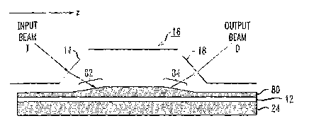
one
case, a linear increase and decrease may be used. FIG. 9 contains simplified
graphs
depicting the thickness variation of the evanescent coupling region in
association with
the amplitude of the optical beams, FIG. 9(a) for the input portion of the
arrangement
of FIG. 8, and FIG. 9(b) for the output portion of the arrangement of FIG. 8.
There are at least three principal advantages of using a tapered evanescent
coupling region, as will be evident from the coupling efficiency results
discussed
below. First, the coupling efficiency at the center wavelength ~,~ is improved
over that
obtained with a constant thickness evanescent coupling layer. In some cases,
the
coupling efficiency can be improved from a value of 80% to approximately 97%.
Thus, a wavelength range sensitivity broadening technique (such as the use of
a
thinner evanescent coupling layer and/or a different material, as discussed
above) may
be used in combination with the tapered evanescent coupling layer to provide
both a
relatively high coupling efficiency at ~,~ and an acceptable level of coupling
efficiency
over an extended wavelength range. Also, when using an evanescent coupling
layer
of varying thickness, the input beam essentially intercepts a variety of
thickness
values. That is, a significant section of the input beam (on the order of 50%)
12
CA 02522045 2005-10-11
WO 2004/097902 PCT/US2004/013128
intercepts evanescent coupling layer thicknesses along input portion 82 that
are less ,,
than the optimal value (the "optimal" being defined as for a constant
thickness
evanescent coupling layer). This is clearly seen in the graphs of FIG. 9(a).
The same
is true for the out-coupled beam as it impinges output coupling portion 84, as
illustrated in FIG. 9(b). Therefore, since at least half of each beam
experiences a
reduced thickness, the wavelength sensitivity is reduced, for the reasons
discussed
above. Finally, since the tapered evanescent coupling region has a high degree
of
mode matching to both the input and output Gaussian beams, the arrangement of
the
present invention is especially convenient to use with conventional
transmitting and
receiving optical elements, such as optical fibers.
FIG. 10 contains a graph illustrating the improvement in coupling efficiency
associated with using a tapered evanescent coupling layer similar to that
shown
schematically in FIG.B. The values for the plots of FIG. 10 were obtained for
a center
wavelength 7~° of 1550 nm and a free space beam diameter two of 63 pm
at the TE
mode polarization state, a silicon dioxide evanescent coupling layer with an
index of
refraction of 1.45 and a prism coupling angle 0pr of 54.74°. Curve A
illustrates, for the
sake of comparison, the coupling efficiency for a constant thickness
evanescent
coupling layer,(similar to the results of curve A illustrated in FIG. 4),
where in this
case the thickness is approximately 320 nm. The plot of curve B is associated
with a
tapered evanescent coupling layer that has been optimized for a center
wavelength of
1550 nm. That is, the taper has been chosen to provide for a maximum coupling
efficiency (in this case, 97.5%) at 1550 nm. It can be shown that for a
linearly
varying tapered portion, the slope associated with this taper is approximately
0.1 °.
Note that the coupling efficiency over the entire wavelength range is improved
when
compared to using a constant thickness evanescent coupling layer. Curve C is
associated with a tapered evanescent coupling layer that is also slightly
reduced in
thickness for all points sampled by the beam (compared to the optimal value),
the
reduction being approximately 40 nm and an increase in slope to approximately
0.15°.
As with curve B, the evanescent layer associated with the measurements for
curve C
also yields coupling efficiencies that are better over the entire wavelength
range than
the coupling efficiency associated with the constant thickness embodiment. For
both
tapered evanescent coupling layers, the coupling efficiency at the outer
regions of the
wavelength range is improved by a factor of 2 to 3. In addition, the coupling
13
CA 02522045 2005-10-11
WO 2004/097902 PCT/US2004/013128
efficiency at the center wavelength ~,° is greater by at least 10 to
20%. Thus, in
accordance with this embodiment of the present invention, the use of an
evanescent
coupling layer of varying thickness can significantly improve the light
transmission
through the associated S~I layer at not only a single wavelength, but over a
predetermined wavelength range. Since the efficiency is improved significantly
at all
wavelengths, it is possible to tailor some of the other device parameters for
a
wavelength range of a specific width. For example, the variation in coupling
efficiency across the wavelength range can be reduced without substantial
reductions
in the efficiency near the center of the band.
The plots of FIG. 11 compare the coupling efficiencies for three different
configurations, all constrained to yield a coupling efficiency of 75% at a
center
wavelength of 1550 nm. Curve A, as shown prior in FIG. 4, illustrates the case
of an
evanescent coupling layer of constant thickness (320 nm), the layer comprising
silicon
dioxide. Curve B is also associated with a constant thickness evanescent
coupling
layer (466 nm), this curve associated with the use of silicon nitride. The
final plot,
curve C, represents a configuration with an evanescent coupling layer of
linearly
varying thickness and refractive index of 1.45 (silicon dioxide). As shown in
FIG. 11,
this last configuration provides the same degree of spectral broadening as is
achieved
by using the higher index material associated with curve B. This is a
significant
result, since a smaller number of materials are required to produce this
arrangement.
Therefore, by tapering the thickness of the evanescent coupling layer, a
silicon
dioxide material layer may be used and perform as well as a layer comprised of
silicon nitride. It is further presumed, moreover, that for those cases where
a material
such as silicon nitride may be used, the combination of a tapered evanescent
coupling
layer with a relatively large index of refraction will even further improve
the coupling
efficiency over the same wavelength range. FIG. 12, for example, contains a
set of
plots for three optimized conditions: curve A associated with using a silicon
nitride
evanescent coupling layer of constant thickness, curve B associated with using
a
silicon dioxide tapered evanescent coupling layer, and curve C associated with
using a
silicon nitride tapered evanescent coupling layer - each curve determined in
association with a center wavelength of 1550 nm. In the latter arrangement, it
should
be noted that the coupling efficiency has been increased on the average of 40 -
50%
over the entire wavelength range.
14
CA 02522045 2005-10-11
WO 2004/097902 PCT/US2004/013128
It should be noted that a beam steering arrangement may be used in
combination with a tapered evanescent coupling layer to further control the
precise
location along the taper where the center of the beam intercepts the
evanescent
coupling layer. Further, another embodiment of an evanescent coupling layer
for
providing reduced wavelength sensitivity can be formed by "grading" the
effective
refractive index of the evanescent coupling layer along the propagation
direction of
the optical signal in the S~I layer. In particular, the refractive index
variation is
modified (graded) so that it tends to equalize the value of ~s; over the
desired
wavelength range. In particular, the effective refractive index may be
realized by
using a dual-layer structure, with a first layer comprising a first material
and formed
to comprise a constant thickness. A second layer, of another material, is
formed as a
taper over the first layer. Thus, the effective refractive index increases
(along the
input) as the signal propagated along the waveguide. In one embodiment, the
tapered
layer may be realized by using alternate layers of materials with appropriate
indexes,
where the layers may be alternated either horizontally or vertically.
It is to be understood that the above-described embodiments of the present
invention are exemplary only, and should not be considered to define or limit
the
scope of the present invention. Indeed, the present invention is most properly
defined
by the claims appended hereto.