Note : Les descriptions sont présentées dans la langue officielle dans laquelle elles ont été soumises.
CA 02526087 2005-11-15
WO 2004/106908 PCT/US2003/015749
SOLID STATE GAS SENSORS BASED ON TUNNEL JUNCTION
GEOMETRY
BACKGROUND OF THE INVENTION
This invention relates to solid state gas sensors. More particularly, this
invention relates to solid state gas sensors for sulfur dioxide. Even more
particularly,
this invention relates to solid state sulfur dioxide sensors using Al-A1203-Au
structures.
Sulfur dioxide (S02)is a gas that is both useful in industrial applications
and an undesired byproduct of some processes. For example, S02 is used to
produce cooking liquors for paper making, but it is also considered a
pollutant from
lime kilns. Government mandates limit the amount of S02 that may be emitted
from
the paper making process.
S02 is also a useful compound in the wine making industry, where it is
used to delay bacterial growth. However, it also is a byproduct of yeast
fermentation
and S02 levels in wine can vary with temperature and pH. This variation may
adversely affect the quality of the final product. Therefore, effective
monitoring and
control of S02 levels is generally recognized as essential to all phases of
wine
making. The standard methods of monitoring S02 have been the Ripper or iodine
method and the vacuum aspiration method. Both of these methods are unsuitable
for testing on location, requiring that samples be taken from a cellar to a
laboratory
for analysis. This may cause a significant delay before corrective dosing, if
necessary,
can be effected.
The Ripper method is also susceptible to several sources of error. Phenolic
substances in red wines, for example, react with the reagent iodine to produce
results that indicate a higher level of S02 than is actually present. The end
point of
this test is also not well defined and the results tend to fade quickly. The
Ripper
method is also susceptible to skewing by ascorbic acid. Additionally, juice
from
UA445 1
CA 02526087 2005-11-15
WO 2004/106908 PCT/US2003/015749
grapes affected by botrytis cannot be accurately measured by iodine titration.
Furthermore the iodine reagent is unstable and must be standardized by
titration
with sodium thiosulphate periodically. Iodine reagent is also extremely
sensitive to
sunlight.
S02 plays a role in many other industries as well. For example, the ability
to minimize emissions of S02 from aircraft may also have an impact on the
ability
of the aerospace industry to develop new supersonic transport vehicles.
Furthermore,
S02 is corrosive of some combustion engine components. S02 has also been shown
to play a role in fouling catalysts used in the automotive and petroleum
industries.
S02 is also generated during the regeneration of sorbents for coal
gasification.
Therefore, there is a need to monitor S02 levels in a wide variety of
industries,
where a lack of appropriate chemical sensors can be a limiting factor for many
technologies. This is especially true in the case of sulfur dioxide (S02)
monitoring.
Recent efforts in the area of gas detection incorporate solid electrolytes,
metal oxides, or polymer coatings as the detectors' active region. Gas
detectors
utilizing solid electrolytes are disclosed in a number of U.S. patents. For
example,
U.S. Patent No. 4,855,034 discloses a sulfur dioxide sensor which utilizes a
solid
electrolyte of a compound of sodium oxide and aluminum oxide (~3-alumina). The
sensor also includes a platinum, lead, or platinum-lead alloy which
accelerates the
reaction of sulfur dioxide with oxygen.
U.S. Patent No. 6,179,992 discloses a gas detection systems that contains
an oxygen ion conducting solid electrolyte and a metallic salt which acts as a
gas
sensitive layer. A cationically conductive material is disposed between the
electrolyte and the gas sensitive material. U.S. Patent No. 6,200,445 also
discloses
a sulfur dioxide sensor that comprises a solid electrolyte that has oxygen ion
conductivity. A detecting electrode is electrically connected to at least part
of the
surface of the solid electrolyte, and a basic electrode is also connected to
at least a
part of the surface of the solid electrolyte. The detecting electrode contains
glass
and either gold or a gold alloy. The basic electrode contains platinum or a
platinum
alloy. The glass component of the detecting electrode is reported to suppress
reaction of inflammable gases such as carbon monoxide. A similar sensor is
also
UA445 2
CA 02526087 2005-11-15
WO 2004/106908 PCT/US2003/015749
disclosed m U.S. Yatent lVO. b,;ibt5,4/y.
U.S. Patent No. 4,718,991 discloses a "proton conductor gas sensor" for
detecting gases, such as sulfur dioxide, which produce protons upon reacting
with
water. The gas sensor comprises a proton conductor which may be antimonic
acid,
zirconium phosphate, dodecamolybdophosphoric acid and the like. Attached to
the
proton conductor is an ionization electrode and a reference electrode. The
ionization and reference electrodes may be platinum, rhodium or other metals.
Silver and gold are also listed as potential materials for the reference
electrode.
The use of metal oxides in gas sensors is also known. For example, the use
of a zirconium oxide probe to measure sulfur dioxide levels in a combustion
system
is disclosed in U.S. Patent No. 4,978,434.
A system utilizing thin film electrodes coated with an electrolyte film is
disclosed in U.S. Patent No. 5,716,506. The thin film electrodes may be
platinum
and the electrolyte film is capable of conducting electricity at room
temperature.
The sensor comprises a substrate which may be silicon dioxide, alumina, or a
polymer, a working electrode deposited on the substrate, a counter electrode
also
deposited on the substrate and a film of polymer electrolyte applied over both
electrodes. The working electrode comprises a first layer of gold, platinum or
carbon
which is in contact with the substrate and a second layer of platinum in
contact with
the first layer. The first layer has a thickness of about 250 to about 5000
angstroms.
Other types of sensors for the selective detection of gases are also known.
U.S. Patent No. 5,841,021, discloses an electrochemical gas sensor for
detecting a
variety of gases including oxides of sulfur. The sensor has an electrode which
reacts
to the presence of the gas in question, a reference electrode which does not
react to
the gas in question, and an electrically conducting substrate which connects
the two
electrodes. A gas sensor is disclosed in U.S. Patent No. 6,165,336 which
utilizes a
gas permeation element which allows the separation of a gas of interest such
as
carbon monoxide from gases that may cause deterioration of the sensor. U.S.
Patent
No. 5,041,204 is directed to an electrochemical method for detecting sulfur
dioxide
UA445 3
CA 02526087 2005-11-15
WO 2004/106908 PCT/US2003/015749
or hydrogen cyanide using copper ions. U.S. Patent No. 5,128,018 is also an
electrochemical apparatus for detecting gases such as sulfur dioxide. This
system
makes use of heteropoly acids or iron salts in an electrolyte in an
electrochemical
measuring cell. U.S. Pat. No. 5,041,204 discloses a electrochemical measuring
cell
for detecting hydrogen cyanide or sulfur dioxide using a pair of electrodes
disposed
in an electrolyte.
The adsorption of S02 onto clean metal surfaces is known. For example,
it is known that room temperature adsorption of S02 on copper surfaces is
dissociative, forming adsorbed S(a), O(a), and SO(a) species. However, a
method
for using gas adsorption onto metal surfaces in connection with tunnel
junction
geometry for devices has not been known.
Therefore, there is a continuing need for alternate methods of detecting
gases such as S02. There is also a need for a gas sensor, especially a sensor
for S02,
that is portable and easy to use. There is a continuing need for detectors
that are
smaller, lighter in weight, and require less power than present day detection
schemes. There is a particular need for S02 detectors in the wine industry
that
provide results with a minimum of delay from the time of taking a sample, and
that
are easy to use.
BRIEF SUMMARY OF THE INVENTION
It is, therefore, an aspect of the present invention to provide a gas sensor
for sulfur dioxide that is portable and inexpensive.
It is another aspect of the present invention to provide a gas sensor that
relies on tunnel junction geometry to detect 502.
It is still another aspect of the present invention to provide a method for
detecting a gas, where the sensor utilizes tunnel junction geometry to detect
a
particular gas or groups of gases.
UA445 4
CA 02526087 2005-11-15
WO 2004/106908 PCT/US2003/015749
At least one or more of the foregoing aspects, together with the
advantages thereof over the known art relating to gas detection, which shall
become
apparent from the specification which follows, are accomplished by the
invention as
herein after described and claimed.
In general, the present invention provides a gas detector comprising a first
electrically conductive material layer, an electrically nonconductive material
layer
disposed on the first electrically conductive material layer; a second
electrically
conductive material layer disposed on the electrically nonconductive material
layer;
a gas source in fluid communication with the second electrically conductive
material
layer; and a power source in electrical communication with the first and
second
electrically conductive material layers.
The present invention also provides a method of detecting a gas, the
method comprising determining the change in impedance of a tunnel junction
device
upon exposure to a gas sample, wherein the tunnel junction device contains a
first
electrically conductive material layer, an electrically nonconductive material
layer
disposed on the first electrically conductive material layer, and a second
electrically
conductive material layer disposed on the electrically nonconductive material
layer,
and wherein the first and second electrically conducting layers are in
electrical
communication with a power source.
A method of making a gas detector is also provided. The method
comprises forming a first electrically conductive material layer, disposing an
electrically nonconductive material layer on the first electrically conductive
material
layer, disposing a second electrically conductive material layer on the
electrically
nonconductive material layer, and placing the first and second electrically
conducting layers in electrical communication with a power source.
BRIEF DESCRIPTION OF THE SEVERAL VIEWS OF THE DRAWINGS
Fig. 1 is a schematic representation of the active surface of the gas sensor
of the present invention.
UA445 5
CA 02526087 2005-11-15
WO 2004/106908 PCT/US2003/015749
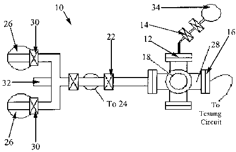
Fig. 2a is a schematic representation of a high vacuum test apparatus
taken from a side view.
Fig. 2b is a schematic representation of a high vacuum test apparatus
taken from a top view.
Fig. 3 is graph showing the magnitude of AC response versus the
magnitude of DC response for gas sensors according to the present invention.
DETAILED DESCRIPTION OF THE INVENTION
The present invention is a gas sensor based on high vacuum evaporated
metal-insulator-metal tunnel junctions and an associated method of testing for
a gas.
The sensor comprises an electrically conductive material layer, such as a
metal or a
metal alloy, as a first layer. An electrically nonconductive material layer is
disposed
on the first electrically conductive material layer and a second electrically
conductive
material layer, such as a metal or metal alloy, is disposed on the
electrically
nonconductive material layer, forming a tunnel junction apparatus.
The first electrically conductive material layer may contain a metal or a
metal alloy. Preferred metals include alkaline earth metals such as magnesium,
transition metals such as chromium, titanium and zirconium, and other metals
such
as aluminum, and their alloys. Aluminum and aluminum alloys are particularly
preferred due to their relatively low cost, low density, and ease of handling.
The
first conductive layer may be any thickness, provided that a uniform, solid
layer is
provided. However, because it is desirable to minimize the weight of the
detector,
the layer may preferably be between about 100 nm and about 500 nm thick. In
one
example, the first layer of conductive material is at least about 200 nm
thick.
The electrically nonconductive or insulating layer is a sufficiently thin
layer so that it acts as an insulator, yet electrons are capable of migrating
through
the material to form a tunnel junction device. In one example, the
nonconducting
layer is between about 2 and about 10 nm thick. Preferred materials for the
UA445
CA 02526087 2005-11-15
WO 2004/106908 PCT/US2003/015749
nonconducting layer include aluminum oxide, magnesium oxide, chromic oxide,
titanium dioxide, zirconium oxide, silicon dioxide, and the like.
The second electrically conductive material layer is disposed on the
electrically nonconductive material layer and preferably is selectively
catalytic for the
gas to be detected. The second electrically conductive material layer may also
have
a strong affinity for at least one catalytic product. For example, gold
selectively
catalyzes S02 dissociation and is permanently contaminated by sulfur after
less
reactive species are removed. Other noble metals such as silver, platinum,
rhodium,
iridium, palladium, ruthenium, and osmium may also be used, depending on the
gas
to be detected. It is also envisioned that alloys and solid solutions of noble
metals
may also be used such as platinum-iridium, palladium-gold, platinum-silver and
palladium-gold. The second conductive layer may be any thickness, provided
that
a uniform, solid layer is provided. However, because it is desirable to
minimize the
weight and cost of the detector, the layer may preferably be between about 100
and
about 500 nm thick. In one example, the second layer of conductive material is
at
least about 200 nm thick. In one particular example, the second layer of
conductive
material has a thickness of about 250 nm.
The first and second electrically conductive materials are placed in
electrical communication with a power source to measure the change in
impedance
upon exposure to the sample. In one example, the power source is a direct
current
(DC) power source. In another example the power source is an alternating
current
(AC) power source. In still another example, both a direct current and an
alternating current power source are placed in electrical communication with
the
conducting layers. The power source preferably provides electrical current
below a
level which will cause the device to heat and eventually short out. In one
example,
the current is no greater than 10 milliamperes (mA) .
In order to demonstrate the practice of the current invention, S02
detectors according to the present invention were synthesized. The following
examples should not be viewed as limiting the scope of the invention. The
claims
will serve to define the inventions. Testing was performed in a high vacuum
test
UA445 7
CA 02526087 2005-11-15
WO 2004/106908 PCT/US2003/015749
stand. It is anticipated that devices according to the present invention will
be used
in environments other than vacuum. The devices were tested under vacuum to
minimize surface contamination, such as that resulting from the adsorption of
volatile hydrocarbons and water vapor from the laboratory air. In these
examples,
both the AC and DC response of the devices using a simple modular design and
circuitry was measured.
The sensing device of the present invention was fabricated in a diffusion-
pumped bell jar system with a base pressure of 10'8 torr. Glass microscope
slides are
cut to fit a substrate holder mounted inside the vacuum system, and then
cleaned by
sonication and rinsing with solvents (reagent grade acetone and isopropyl
alcohol).
The patterned geometry of the test devices as shown in Fig. 1 is transferred
to the
glass substrates by thermal evaporation through arc-machined stainless steel
masks.
In the present case, A1 (99.999 % pure) is evaporated at pressures in the 10-'
torr
range to a thickness greater than 200 nm to form the base electrode. A thin
film of
insulating alumina is then grown on the surface of the A1 electrode by
exposure to
a DC oxygen glow discharge (nominally 100 mtorr, 550 V, 275 mA) for
approximately 30 minutes. The sample stage is then rotated to place the
substrate
over a second evaporation station, where Au (99.999 % pure) cover electrodes
are
evaporated. The thickness of the gold films can be measured by a quartz
crystal
thickness monitor and is approximately 250 nm for the data presented here.
After the evaporation and oxidation steps are complete, the vacuum
system is vented with dry nitrogen and the samples transferred to the test
stand for
electrical measurements. However, the relative humidity when we open the
chamber affects the composition of the background gas present when the next
sample is fabricated, and differences in the hydroxyl content of the alumina
films
will manifest themselves as scatter in our data. Note in Fig. 1 that each
evaporation
sequence produces three independent tunnel junctions, each with a different
cross
sectional area. The data presented herein demonstrate that these geometric
factors
do not play a role in the sensing capabilities of the structures, and
therefore, that this
concept of using tunnel junctions as gas sensors is transferable to other
fabrication
technologies and geometries. Note also that the spacing of the leads is
matched to
UA445
CA 02526087 2005-11-15
WO 2004/106908 PCT/US2003/015749
that of a RS Components printed circuit board edge connector (#466-539) so
that
the devices plug directly into the connector. This circumvents making
electrical
connections to the samples by hand and facilitates the transfer process
between
vacuum systems.
As illustrated in Fig. 2, we have constructed a sorption-pumped high
vacuum system specifically for testing these gas sensors. The test stand (10)
is an
all stainless steel system with copper-gasket sealed fittings and bakeable
valves. The
testing chamber (28) is a six-way cross which accepts 4.5 inch OD Confiat
flanges,
and is large enough to accommodate the detectors while also enclosing the
smallest
volume possible to limit the amount of S02 gas used. One of the ports (12) on
the
chamber allows for gas entry through a bellows valve (14). Another port (16)
provides for sample mounting in the edge connector. Another port (18) is for
pressure measurement in the 10-2 - 10-' torr range with a capacitance
manometer
(Baratron) (20), and another port leads through a gate valve (22) to the
pumps.
The chamber (28) is pumped by a mechanical roughing pump (24) in
parallel with two sorption pumps (26). In normal operation, the device to be
tested
is plugged into the edge connector and the flange is then mounted on the test
chamber using a new copper gasket. The sorption pumps (26) are isolated by
right
angle bellows valves (30) and cooled with liquid nitrogen while the roughing
pump
(24) is used to bring the system to approximately 10-2 torr as measured by a
Pirani
gauge (32). The mechanical pump (24) is then isolated and shut off and the
sorption pumps (26) bring the test chamber to the 10-$ torr range where the
manometer is zeroed. This procedure provides a hydrocarbon-free environment
void
of mechanical or electrical noise in which the devices are tested.
Testing is performed by leaking S02 into the chamber and then removing
it by pumping with the sorption pumps. The corrosive gas is trapped by the
large
surface area molecular sieve within the cooled pumps so there is no exhaust
and
testing can be performed without a fume hood or exhaust-gas handling system. A
null bridge with decade resistors and capacitors was used for monitoring
changes in
the electrical response of the devices due to exposure to 502. A voltage
divider was
UA445 9
CA 02526087 2005-11-15
WO 2004/106908 PCT/US2003/015749
used to limit the total current, as currents above the 10 mA range in this
apparatus
cause heating and eventual shorting out of the devices. These small currents
in turn
yield small voltage drops across the junctions which add to scatter in the
resulting
data. A multipole switch was used to rotate the measurements between the three
junctions during testing. Steady state results reflecting net changes in the
electrical
properties of the devices due to integrated exposure to S02 gas are reported.
Figure 3 presents data following adsorption of S02 onto the gold surfaces
of the tunnel junctions at room temperature (approximately 300 K). The S02
exposure and glow discharge times for each of these eight samples are
essentially the
same, but they are fabricated over about a one month time frame. The data from
three junctions on each sample are averaged in Fig. 3 (unless a junction is
shorted)
since the electrical response presented in this manner is independent of the
cross
sectional area of the junctions as discussed below. The data cluster around a
linear
trend line. If all the fabrication conditions were exactly the same for all
samples, the
data of Fig. 3 (collected at fixed frequency) would be expected to lie at the
same
coordinates. However, humidity variations in the growth chamber influence the
hydroxyl content and thus the conductivity and permittivity of the oxide
layers. The
data in Fig. 3 shows that these electrical properties vary proportionally to
one
another as discussed more fully below.
The data indicate that the devices respond to S02 exposure pressures in
the 10-2 torr range. Ideally, a gas detector will respond only to S02 and not
to other
gases. This would imply that at atmospheric pressures on the order of 103 torr
these
detectors would respond to S02 concentrations of about one part in 105. This
level
of detection demonstrates that a tunnel junction geometry for devices will
operate
as gas sensors for S02.
There is a simple way to understand why the data of Fig. 3 should follow
a linear trend and be independent of the cross sectional area of the junctions
if one
considers the junction region as a leaky parallel plate capacitor and neglects
the
impedance of the connecting leads. The AC voltage response is proportional to
the
inverse of the capacitance of the junction,
UA445 10
CA 02526087 2005-11-15
WO 2004/106908 PCT/US2003/015749
VAC « d
~A (1)
where d and A are the thickness and cross-sectional area of the insulator
layer
forming the junction, respectively and E is its effective dielectric constant.
The DC
voltage response of the junction also involves its geometric properties and
its
electrical conductivity, Q,
uDC ~ d
QA (2)
so that the ratio of the two voltages which represents the slope of the line
shown in
Fig. 3 is
Vc ~ Q
VDC ~ . (3)
This ratio is constant at fixed frequency (c~) assuming a standard model such
as
E(c~)=E°(c~)+4~i Q~
where we interpret E(c.~)- E°(c~) as the effective dielectric constant
E in Eq. (3). This
demonstrates why E and a should vary proportional to one another as the
hydroxyl
content of the oxide layers varies from sample to sample, and thus why we
expect
the data of Fig. 3 to cluster around a linear trend line.
As mentioned above, the adsorption of S02 onto clean metal surfaces, such as
gold,
is known. Sulfur is also a known natural contaminant of gold. In the present
apparatus, the gold surface acts to catalyze S02 dissociation and is
permanently
contaminated (poisoned) by sulfur after the weakly bound species are pumped
away.
The process of chemisorption involves electron transfer and redistribution
processes
which alter the DC and AC impedance of the devices and thus the voltages
measured
across the tunnel junction.
This effect is distinctly different from other gas sensor designs that use
UA445 11
CA 02526087 2005-11-15
WO 2004/106908 PCT/US2003/015749
gold electrodes (such as those for NOZ) since in that case there is no
dissociation and
thus no permanent modification of the structures. In the present invention,
the
ability to reuse the device is conceded, but given the simplicity and low
fabrication
cost of the present invention, this is an acceptable trade-off. It is believed
that the
present invention will also work for other sulfur containing compounds that
dissociate on gold. However, the gas detector of the present invention should
not
be influenced by reactions with common atmospheric gases such as oxygen and
carbon dioxide since these do not dissociate on gold surfaces. In summary, we
have
shown that a tunnel junction configuration can be used as the basis for a
detector
of integrated S02 exposure.
Based upon the foregoing disclosure, it should now be apparent that
gas detectors utilizing tunnel junction geometry will carry out the objects
set forth
hereinabove. It is, therefore, to be understood that any variations evident
fall within
the scope of the claimed invention and thus, the selection of specific
component
elements can be determined without departing from the spirit of the invention
herein
disclosed and described.
UA445 12