Note : Les descriptions sont présentées dans la langue officielle dans laquelle elles ont été soumises.
CA 02527602 2005-11-29
WO 2004/111706 PCT/US2004/017449
MICRO-LENS AR~t AY WITH PRECISELY ALIGNED APERTURE MASK AND
METHODS OF PRODUCING SAME
BACKGROUND OF THE INVENTION
This Application is a Continuation-in-part of Application No. 10/120,785 filed
April
12, 2002, which is a Continuation-in-part of U.S. Application Serial No.
09/521,236, filed
April 5, 2000, now U.S. Patent No. 6,483,612, which is a Continuation of U.S.
Application
Serial No. 08/060,906, filed April 15, 1998, now abandoned. The entire
disclosures of the
prior applications are incorporated herein by reference.
1. Field of the Invention
[1] The present invention relates to lenses, and particularly relates to micro-
lens
arrays.
2. Background of the Related Art
[2] Micro-lens arrays have found increasing application in a wide variety of
fields,
from ophthalmology through displays. Individual lenses, or lenslets, in the
arrays can have
sizes ranging from 1 ~.m to 10 mm in diameter.
[3] In many applications, it is desirable to produce micro-lens arrays in
which a
mask or field stop is aligned with the lenses. The mask may include a
plurality of apertures
that ~e aligned with the individual lenses in the array. The purpose of such a
mask map
include reducing crosstalk or interference between the images created by each
lenslet, or
1
CA 02527602 2005-11-29
WO 2004/111706 PCT/US2004/017449
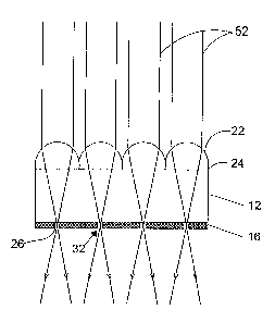
modifying or improving the optical characteristics and performance of the
lenslets by
altering the affective aperture. Masks can also be useful in reducing
reflected light and
improving the contrast of the images created by the array.
[4] Given the potentially large number of lenses in micro-lens array, and the
micron-scale size of the lenses in some applications, it is very difficult to
effectively and
precisely align the pattern of apertures in the mask with the exit pupils of
the lenses.
Currently available techniques include registration of the mask with the lens
array using
fiducials or similar methods borrowed from semiconductor mask or printing
technology.
These techniques are difficult to employ accurately over large areas and are
time-consuming
and expensive.
[5] Alternative methods involve applying mask material to the lens array using
an
adhesive cured by exposure to ultraviolet light.
SUMMARY OF THE INVENTION
[6] An object of the invention is to solve at least the above problems and/or
disadvantages and to provide at least the advantages described hereinafter.
(7] Another object of the invention is to provide a lenslet of a micro-lens
array
with an aligned aperture.
[8] Another object of the invention is to provide a plurality of lenslets with
a
plurality of aligned apertures, the plurality of lenslets forming a micro-lens
array.
[9] Another object of the invention is to provide a micro-lens array with a
mask
including aligned apertures attached thereto.
2
CA 02527602 2005-11-29
WO 2004/111706 PCT/US2004/017449
[10] Another object of the invention is to provide a micro-lens array on a
first
substrate, and a mask having apertures on a second substrate that is attached
to the first
substrate, with the apertures aligned with corresponding lenslets in the micro-
lens array.
[11] Another object of the invention is to provide a method of manufacturing a
lenslet of a micro-lens array with an aligned aperture.
[12] Another object of the invention is to provide a method of manufacturing a
micro-lens array on a first substrate, and a mask having apertures on a second
substrate that
is attached to the first substrate, with the apertures aligned with
corresponding lenslets in the
micro-lens array.
[13] Another object of the invention is to provide a method of manufacturing a
micro-lens array with a mask including aligned apertures attached thereto.
[14] To achieve these and other objects, a method of fabricating a lens with
an
afigned aperture is provided, comprising attaching a mask material to a lens,
and projecting
electromagnetic radiation onto the mask material with the lens, wherein the
intensity of the
electromagnetic radiation and the mask material are chosen so that an aperture
is formed in
the mask material by the electromagnetic radiation via a non-ablative process.
[15] To further achieve these and other objects, there is further provided
method
of fabricating a micro-lens array with an aligned aperture mask, comprising
providing a first
substrate, forming a micro-lens array on a first surface of the fast
substrate, wherein the
micro-lens array comprises a plurality of lenslets, applying a mask material
to a second
surface of the first substrate, and projecting electromagnetic radiation onto
the mask material
with each lenslet, wherein the intensity of the electromagnetic radiation and
the mask
J
CA 02527602 2005-11-29
WO 2004/111706 PCT/US2004/017449
material are chosen so that apertures are formed in the mask material by the
electromagnetic
radiation via a non-ablative process.
[16] To further achieve these and other objects, there is further provided a
method
of fabricating a micro-lens array with an aligned aperture mask, comprising
providing a first
substrate, forming a micro-lens array on a first surface of the first
substrate, wherein the
micro-lens array comprises a plurality of lenslets, applying a mask material
to a first surface
of a second substrate, attaching a second surface of the first substrate with
the first suiface
of the second substrate, and projecting electromagnetic radiation onto the
mask material
with each lenslet, wherein the intensity of the electromagnetic radiation and
the mask
material are chosen so that apertures are formed in the mask material by the
electromagnetic
radiation via a non-ablative process.
[17] To further achieve these and other objects, there is further provided an
optical
system, comprising a micro-lens array comprising a plurality of lenslets and
an aperture mask
in optical communication with the micro-lens array, wherein the aperture mask
comprises a
plurality of apertures aligned with respective lenslets of the micro-lens
array that are formed
with a non-ablative process.
[1~] To further achieve these and other objects, there is further provided an
optical
system, comprising a lens and an aperture mask in optical communication with
the lens,
wherein the aperture mask comprises an aperture aligned with the lens, that is
formed with a
non-ablative process.
[19] Additional advantages, objects, and features of the invention will be set
forth
in part in the description which follows and in part will become apparent to
those having
4
CA 02527602 2005-11-29
WO 2004/111706 PCT/US2004/017449
ordlnarp sxlu In the art upon examination of the following or may be learned
from practice
of the invention. The objects and advantages of the invention map be realized
and attained
as particularly pointed out in the appended claims.
BRIEF DESCRIPTION OF THE DRAWINGS
[20) The invention will. be described in detail with reference ~to ' the
following
drawings in which like reference numerals refer to like elements wherein:
[21) Figure 1 is a perspective view of lenslets in a micro-lens array;
[22] Figure 2.A is a perspective view of a micro-lens array with an aligned
aperture
mask, in accordance with one preferred embodiment of the present invention;
[23) Figure 2B is a cross-sectional view of fihe micro-lens array with aligned
aperture mask embodiment of Fig. 2A, in accordance with the present invention;
[24) Figure 2C is a plan view of the aperture mask used in the embodiment of
Figs.
2A and 2B, in accordance with the present invention;
[25] Figure 2D is a cross-sectional view of the micro-lens array with aligned
aperture mask embodiment of Figs. 2.A-2C, showing how light . propagates
through the
micro-lens array/aperture mask combination, in accordance with the present
invention;
[26] Figure 2E is a perspective view of a micro-lens array with an aligned
aperture
mask, in accordance with the present invention;
[27] Figure 2F is a plan view of the aperture mask used in the embodiment of
Fig.
2E, in accordance with the present invention;
CA 02527602 2005-11-29
WO 2004/111706 PCT/US2004/017449
[28] Figure 3A is a perspective view of a micro-lens array with an aligned
aperture
mask, in accordance with a second preferred embodiment of the present
invention;
[29] Figure 3B is a cross-sectional view of the micro-lens array with aligned
aperture mask embodiment of Fig. 3A, in accordance with the present invention;
[30] Figures 4A-4D are cross-sectional views of steps in one preferred method
of
fabricating a micro-lens axray/aperture mask, in accordance with the present
invention;
[31] Figures 5A-5E are cross-sectional views of steps in another preferred
method
of fabricating a micro-lens array/aperture mask, in accordance with the
present invention;
[32] Figure G is a plan view of a mask portion corresponding to a single
lenslet
section of a micro-lens array before an aperture is formed, in accordance with
the present
invention; and
[33] Figure 7 is a plan view of a mask portion corresponding to a single
lenslet
section of a micro-lens array after an aperture is formed, in accordance with
the present
invention.
DETAILED DESCRIPTION OF PREFERRED EMBODIMENTS
[34] Referring to Figure 1, a micro-lens array 10 made up of an assembly of
lenslets
22 is shown. The lenslets 22 may be formed by "stamping" or embossing lens
material 15.
"Stamping", as used herein; broadly covers the process of forming shapes on a
photopolymer, and curing the photopolymer material, and "stamper" broadly
covers any
tool used to form such shapes. A stamping operation of dlis type is described
in U.S. Patent
G
CA 02527602 2005-11-29
WO 2004/111706 PCT/US2004/017449
Application Serial Number 10/ , , (Attorney Docket No. BVT-0010C1P4), the
contents of which is incorporated herein by reference.
[35~ The lenslets 22 shown in Fig. 1 are convex-shaped, however, other shapes
and
configurations may also be used. In the example shown in Fig. 1, each of the
lenslets 22 has
a spherical sector or a like-rounded projecting portion, and a periphery 23.
However, the
projecting portion of the lenslets map be of any shape, including ellipsoidal,
toroidal or
aspherical. Each lenslet 22 map be hexagonal in shape at its periphery 23, or
other shapes
besides hexagonal could be used for the periphery 23 of each lenslet. The
periphery 23
defines the lenslets 22 as being only partially spherical or partially rounded
surfaces. For
.example, lenslets 22 map form hemispheres. Lenslets 22 map be spaced at
periodic or
random intervals across the surface of the substrate 12.
[36] Referring to Figures 2A-2D a micro-lens array 10 with an aligned aperture
mask 16 is shown in accordance with one preferred embodiment of the present
invention.
In one preferred embodiment, the micro-lens array 10 includes lenslets 22 that
are formed
on or attached to a substrate 12, which has first and second surfaces, 24 and
26, respectively.
Although the lenslets 22 and the substrate 12 are shown as separate elements,
it should be
appreciated that the substrate 12 could be the lens material 15 from which the
lens array 10
is formed, as shown in the lens array 10 of Fig. 1.
[37~ Possible spacing patterns of the lenslets 22 include having at least some
of the
lenslets 22 abutting one another, separating at least some of the lenslets 22
by a prescribed
distance, and/or having at least some of the lenslets 22 overlap each other.
The lenslets 22
7
CA 02527602 2005-11-29
WO 2004/111706 PCT/US2004/017449
can each have similar focal lengths, or their focal lengths can vary from one
another in a
prescribed manner.
[38] The configuration of each of the lenslets 22 may include virtually any
lens
geometry known in the art which may be attached to or formed on the surface of
the planar
substrate 12. . Although not required, the first and second surfaces, 24 and
26, of the
substrate 12 are typically parallel to one another. The overall form of the
planar substrate 12
map be disk-like or sheet-like, although virtually any geometric form can be
used. The planar
substrate 12 is typically made of glass or plastic, although any transparent
material suitable
for micro-lens structures known in the art map be employed.
[39] As shown in Figure 2B, each lenslet 22 will typically have an optical
axis A,
and the optical axis will typically be orthogonal to a planar surface of the
substrate 12.
Although the typical micro-lens array 10 is generally configured so that the
optical axes A of
all the lenslets 22 axe parallel to one another, this need not be the case.
Other configurations
are possible, depending on the application.
[40] Attached onto or positioned adjacent to a second surface 26 of the
substrate
12 is an aperture mask 16. The aperture mask 16 is preferably formed from a
material that is
compatible with a non-ablative aperture formation process, as will be
explained in more
detail below. Preferred mask 16 materials include carbides, such as TiC,
metals (e.g., Al, Cr,
Cu, Zn, Se, Fe) alone or in combination with their oxides, high temperature
metals (e.g., Ti,
Ta, Zr, ~, nitzi.des, oxides, selenides, tellurides, and carbon. Cermets and
mixtures of these
materials may also be used. Preferred mask 16 materials may also include
polymers, organic
black materials, and other substances substantially opaque to the
electromagnetic radiation to
8
CA 02527602 2005-11-29
WO 2004/111706 PCT/US2004/017449
be transmitted by the micro-lens array 10. Typical thicknesses of the mask 16
are on the
order of 0.5 to 100 absorption lengths, depending on the desired optical
properties, although
other thicknesses may be used.
[41] The aperture mask 16 includes a plurality of apertures 32. The aperture
mask
16 preferably has one aperture 32 for each lenslet 22 in the micro-lens array
10, with each
aperture 32 precisely aligned with its respective lenslet 22 so that light
input to a lenslet 22 is
focused through its corresponding aperture 32.
(42] Figure 2C is a plan view of the aperture mask 16, showing the spaced
apertures 32 in the aperture mask 16. Referring to Figure 2D, a micro-lens
array 10 with an
aligned aperture mask 16 is shown with light 52 projected therethrough. As
shown in Figure
2D, when light 52 is directed through a lenslet 22, the lenslet 22 focuses and
directs the light
52 so that at least a portion of it propagates through the aperture 32. Thus,
after the light 52
is refracted by a lenslet 22, the light 52 map be further affected by the
corresponding
aperture 32. Consequently, after passing through the lenslet 22, the light 52
can be further
modified by the aperture 32. Such modifications include blocking a portion of
the light 52,
as well as reducing cross-talk between light 52 input to multiple lenslets 22.
[43] It should be noted that lenses of virtually any geometry may be used with
the
aperture mask. For example, referring to Figures 2E and 2F, a lenticular micro-
lens array 11
is shown. The lenticular micro-lens array 11 includes a subsi~ate 12 with a
top surface 24
and a bottom surface 25. Attached to the top surface 24 are lenticular
lenslets 23 consisting
of linear lens structures. The bottom surface 25 of the substrate 12 has an
aperture mask 17.
The aperture mask 17 has apertures 33 which are aligned with each
corresponding lenslet 23.
9
CA 02527602 2005-11-29
WO 2004/111706 PCT/US2004/017449
[44] Referring to Figure 2F, a plan view of the mask side of the lenticular
lens array
is shown. The lenticular lens array includes the mask 17 with the apertures
33. As can be
seen in Figure 2F, the apertures 33 of the lenticular lens array includes
substantially linear
openings in the mask 17. The apertures 33 run along the substrate 12
substantially in
alignment with each corresponding lenslet 23.
[45] Figures 3A and 3B illustrate a second preferred embodiment of the
invention
is shown. The embodiment of Figs. 3A and 3B is similar to the embodiment of
Figs. 2A-
2D, with the addition of a substrate 28 that is attached to the aperture mask
16. While
preferably transparent to the electromagnetic radiation that will be input to
the micro-lens
array 10, the substrate 28 may also be reflective, partially reflective or
diffusive to the
electromagnetic radiation that will be input to the micro-lens array 10. Thus,
the substrate
28 may provide mechanical support to the micro-lens array 10, protect the
aperture mask 16
and/or filter, polarize or otherwise modify light projected by the lenslets 22
through the
apertures 32.
[46] Figures 4A-4D are cross-sectional views of steps in one preferred method
of
fabricating the micro-lens array/aperture mask of the present invention. For
illustrative
purposes, cross-sectional views showing the formation of two lenslets and
corresponding
apertures are shown. An initial step of the method is forming the micro-lens
array (Fig. 4A),
which includes providing a substrate 12 made of, for example, a polycarbonate
or acrylic
plastic thick enough to provide a desired level of mechanical stability. A
material from
which the micro-lens array is to be replicated on a surface 24 of the
transparent substrate 12
is then applied to the substrate 12 (not shown). This material map be, for
example, a
CA 02527602 2005-11-29
WO 2004/111706 PCT/US2004/017449
photopolymer epoxy, a polycarbonate, or PMMA resin. This material is then
patterned to
form the individual lenses 22 in the micro-lens array. This patterning step
map be performed
by any one of a variety of methods. The patterning step map be performed in
accordance
with a stamping operation performed by a master, which contains the lens
pattern thereon.
A stamping operation of this type is described in U.S. Patent Application
Serial Number
10/ , (Attorney Docket No. BVT-0010C1P4), the contents of which are
incorporated
herein by reference. The patterning step may also be performed by embossing or
other
techniques.
[47] A second step (Fig. 4B) includes coating a second surface 16 of the
substrate
12 with a thin layer 16 of masking material. The thickness of this layer may
vary with the
material employed, but a thickness of from 0.5 to 100 absorption lengths has
been found to
be preferable. Coating techniques include e-beam vacuum deposition,
sputtering, chemical
vapor deposition, as well as other film-deposition techniques. As discussed
above, preferred
masking materials include carbides, such as TiC, metals (e.g., Al, Cr, Cu,
Vin, Se, Fe) alone or
in combination with their oxides, high temperature metals (e.g., Ti, Ta, Zr,
~, nitrides,
oxides, selenides, tellurides, and carbon. Cerinets and mixtures of these
materials may also
be used. Preferred masking materials may also include polymers, organic black
materials,
and other substances substantially opaque to the electromagnetic radiation to
be transmitted
by the micro-lens array 10. Essentially, any substance substantially opaque to
the
electromagnetic radiation to be transmitted by the micro-lens array and that
is compatible
with a non-ablative aperture formation process map be used.
11
CA 02527602 2005-11-29
WO 2004/111706 PCT/US2004/017449
[48] A third step (Fig 4C) includes forming apertures 32 in mask layer 16
which
are aligned with respective lenslets 22. This is preferably performed by
directing pulsed laser
radiation or similarly intense electromagnetic radiation 62 through the curved
surface of each
lenslet 22, which focuses the radiation 62 to an area 42 on the mask layer 16.
The
electromagnetic radiation 62 is preferably pulsed with energy sufficient to
form an aperture
by means of a non-ablative process, but preferably not so much energy so as to
vaporize the
material or degrade the desired optical properties of the lenslets 22 and/or
the associated
substrates.
[49] A typical range for pulses would include irradiance levels above 0.1
mJ/cmz
and pulse widths shorter than 1 ms, however, the precise combination of
irradiance and
pulse widths required will depend on many parameters, including the type of
material used
for the mask layer 16 the thickness of the mask layer and the precise
positioning of the
aperture. For example, for a mask layer 16 made of TiC material with a
thickness in the
range of 0.5 to 100 absorption lengths, a combination of pulses with
irradiances of 1 mJ/cm2
to 5 mJ/cm2 and pulse widths on the order of 10 ns have proven effective.
Additionally, the
optimum wavelengths of the electzomagnetic radiation 62 used will depend on
the spectral
absorption properties of the material used for the mask layer 16. For a mask
layer 16 made
of TiC, a wide range of wavelengths, from infrared through ultraviolet have
proven effective.
[50] The apertures 32 may be formed one at a time by serially illuminating
each
lenslet 22 in the micro-lens array with the pulsed laser radiation, or other
electromagnetic
radiation. Alternatively, they may also be formed by simultaneously
illuminating two or
more of the lenslets 22, using either separate electromagnetic beams (e.g.,
separate pulsed
12
CA 02527602 2005-11-29
WO 2004/111706 PCT/US2004/017449
laser beams) or a single electromagnetic beam (e.g., a single pulsed laser
beam) that has been
spatially expanded to cover two or more of the lenslets 22.
[51] Because the lenslet 22 focuses the laser radiation 62 onto the mask layer
16,
the thickness of the substrate 12 can determine whether the mask layer 1G lies
at the focal
point of the lenslet 22. By using a substrate 12 of a different thickness, the
size of the
irradiated area 42, and therefore the size of the aperture, map be changed.
The smallest
aperture 32 that can be formed by the lenslet is achieved by adjusting the
thickness of the
substrate 12 so that the mask layer 16 lies at the focal plane of the lenslet
22. In this case,
the aperture size is dictated by the diffraction limited spot size of the
radiation at the focal
plane and any aberrations that map be present.
[52] The term "non-ablative process" is used to describe a process in which
apertures are patterned in a mask layer by depositing sufficient
electromagnetic energy at
desired points on the mask layer so that at least one of the following
mechanisms takes
place: (1) a "contraction" mechanism in which the mask layer material heats up
and
contracts to form an aperture without vaporizing or ablating the mask layer
material; (2) a
"phase change" mechanism in which the mask layer material undergoes a phase
change into
a form which is substantially transparent to radiation at desired
predetermined wavelengths;
(3) a "mechanical deformation" mechanism in which the mask layer material
undergoes
mechanical deformation; and/or (4) a "chemical" mechanism in which the mask
layer
material undergoes a chemical transformation, such as oxidation.
[53] With the "contraction" mechanism, the mask layer material is preferably
heated to a point in which the surface tension of the mask layer material
overcomes the
13
CA 02527602 2005-11-29
WO 2004/111706 PCT/US2004/017449
strength of the mask layer material. This results in the mask layer material
"pulling back" or
contracting to form a clear aperture, with rolled back material at the
perimeter of the
aperture. Depending on the mask layer material, it may not be necessary to
heat the mask
layer area where the aperture is to be formed to fihe melting point of the
mask layer material.
[54] With respect to "mechanical deformation" mechanism, localized heating
causes a localized piston effect, in which the mask layer material essentially
explosively
expands, resulting iri an aperture being formed. Mask layer material from the
center of the
aperture formation area is either blown clear off the substrate or off to the
side.
[55] ~ The non-ablative process used in the present invention exhibits many
benefits
over traditional ablative processes. If an ablative process were to be used to
create the
apertures, the mask layer material would have to be heated to the material's
boiling
temperature. In order to achieve these high temperatures, a very high power
laser with very
short laser pulses would have to be used. Lasers that produce pulse widths of
less than 1 ns,
and typically pico-second pulses, are needed for ablative processes. These
types of lasers are
expensive, difficult to work with, and have limited wavelength ranges.
[56] Because ablative processes require the mask layer material to be raised
to the
boiling point, mask layer materials with relatively low boiling temperatures
would need to be
used in order to avoid heating the surrounding areas (e.g., the substrate and
lenslets) to the
point where these areas would be damaged. This would effectively limit the
choice of
materials for the mask layer.
[57] In contrast, the non-ablative process used in the present invention does
not
require that the mask layer material be heated to the material's boiling
point. Accordingly, a
14
CA 02527602 2005-11-29
WO 2004/111706 PCT/US2004/017449
much wider selection of materials can be used in the present invention,
including many high
temperature materials, as listed above. In addition, a wider selection of
radiation sources
may be used with the non-ablative process used in the present invention.
[58] An optional fifth step (Fig. 4D) includes attaching a substrate 28 of
polycarbonate or other material to the mask layer 16 preferably with an
optical adhesive. The
substrate 28 map be optically active and/or map merely serve to protect the
mask layer 16
and provide additional mechanical support to the micro-lens array.
[59] Figures 5A-5E are cross-sectional views of steps in a second preferred
method
of fabricating the micro-lens array/aperture mask of the present invention. An
initial step of
the method (Fig. 5A), a substrate is provided that is made of, for example,
polycarbonate or
acrylic plastic thick enough to provide a desired level of mechanical
stability. The substrate
28 is preferably optically transparent to the electromagnetic radiation that
will be input to the
completed micro-lens array.
[60] A second step (Fig. 5B) includes applying a mask layer 16 to the
substrate 28
using techniques similar to those discussed above in connection with the
method of Figs.
4A-4D.
[61] A third step (Fig. 5C) involves forming the micro-lens array, which
includes
providing a substrate 12 made of, for example, a polycarbonate or acrylic
plastic thick
enough to provide a desired level of mechanical stability. The substrate 12 is
preferably
attached to the mask layer 16 with an optical adhesive.
[62] A material from which the micro-lens array is to be replicated on a
surface 24
of the transparent substrate 12 is then applied to the substrate 12 (not
shown). This material
CA 02527602 2005-11-29
WO 2004/111706 PCT/US2004/017449
map be, for example, a photopolymer epoxy, a polycarbonate, or PlYIM.A resin.
This material
is then patterned to form the individual lenses 22 in the micro-lens array.
This patterning
step may be performed by any one of a variety of methods. Preferably, the
patterning step is
performed in accordance with a stamping operation performed by a master, which
contains
the lens pattern thereon. A stamping operation of this type is described in
U.S. Patent
Application Serial Number 10/ , , (Attorney Docket No. BVT-0010C1P4), the
contents of which are incorporated herein by reference.
[63] A fourth step (Fig. 5D and 5E) includes forming apertures 32 in mask
layer 16
which are aligned with respective lenslets 22. As discussed above, this is
preferably
performed by directing pulsed laser radiation or similarly intense
electromagnetic radiation
62 through the curved surface of each lenslet 22, which focuses the radiation
62 to an area
42 on the mask layer 16. The electromagnetic radiation 62 is preferably pulsed
with energy
sufficient to form an aperture by means of a non-ablative process, but
preferably not so
much energy as to vaporize the material or degrade the desired optical
properties of the
lenslets 22 and/or the associated substrates.
[64] As discussed above, a typical range for pulses would include irradiance
levels
above 0.1 mJ/cm2 and pulse widths shorter than 1 ms, however, the precise
combination of
irradiance and pulse widths required will depend on many parameters, including
the type of
material used for the mask layer 1G the thickness of the mask layer and the
precise
positioning of the aperture. For example, for a mask layer 16 made of TiC
material with a
thickness in the range of 0.5 to 100 absorption lengths, a combination of
pulses with
irradiances of 1 mJ/cm2 to 5 mJ/cm~ and pulse widths on the order of 10 ns
have proven
16
CA 02527602 2005-11-29
WO 2004/111706 PCT/US2004/017449
effective. Additionally, the optimum wavelengths of the elect~oinagnetic
radiation 62 used
will depend on the spectral absorption properties of the material used for the
mask leper 16.
For a mask layer 16 :made of TiC, a wide range of wavelengths, from infrared
through
ultraviolet have proven effective.
[65] The apertures 32 may be formed one at a time by serially illuminating
each
lenslet 22 in the micro-lens array with the pulsed laser radiation, or other
electromagnetic
radiation. Alternatively, they map also be formed by simultaneously
illuminating two or
more of the lenslets 22, using either separate electromagnetic bearns~ (e.g.,
separate pulsed
laser beams) or a single electromagnetic beam (e.g., a single pulsed laser
beam) that has been
spatially expanded to cover two or more of the lenslets 22.
[66] Because the lenslet 22 focuses the laser radiation 62 onto the mask layer
16,
the thickness of the substrate 12 can determine whether the mask lager 16 lies
at the focal
plane of the lenslet 22. By using a substrate 12 of a different thickness, the
size of the
irradiated area 42, and therefore the size of the aperture, map be changed.
The smallest
aperture 32 that can be formed by the lenslet is achieved by adjusting the
thickness of the
substrate 12 so .that the mask layer 16 lies at the focal plane of the lenslet
22. In this case,
the aperture size is dictated by the diffraction lhni.ted spot size of the
radiation at the focal
plane.
[67] As discussed above, the term "non-ablative process" is used herein to
describe
a process in which apertures are formed or patterned in the mask layer,
preferably without
vaporizing or ablating the mask layer material. Use of such a process is of
particular
importance in the fabrication method of Figs. 5A-5E, since the mask leper 16
i.s positioned
17
CA 02527602 2005-11-29
WO 2004/111706 PCT/US2004/017449
between other layers of material (e.g., the two substates 12 and 28). An
ablative process is
particularly inappropriate for this embodiment.
[68] This non-ablative aperture formation process is illustrated in Figs. 5
and 6,
which are plan views of a mask portion corresponding to a single lenslet
section of a micro-
lens array before and after an aperture is formed, respectively.
[69] As shown in Fig. 6, the electomagnetic radiation has been focused onto an
area 42 on the mask layer 16. The energy delivered to the area 42 is
controlled so as to
initiate a non-ablative aperture formation process. In one embodiment of such
a non-
ablative process, an amount of electromagnetic energy is deposited at desired
areas on the
mask layer 16 sufficient to melt the mask layer material and cause it to
contact to form an
aperture 32, as shown in Fig. 7. The shape of the aperture 32 will depend on
the spatial
profile of that portion of the electomagnetic radiation that deposits the
requited amount of
energy on the mask layer 16. Although the aperture 32 shown in Fig. 7 is
generally circular
in shape, any other aperture shape can be produced while still falling within
the scope of the
present invention, including, but not limited to, square, rectangular,
polygonal and elliptical
shapes.
[70] Other modifications and variations to the invention will be apparent to
those
skilled in the art from the foregoing disclosure. Thus, while only certain
embodiments of the
invention have been specifically described herein, it will be apparent that
numerous
modifications map be made thereto without departing from the spirit and scope
of the
invention.
18