Note : Les descriptions sont présentées dans la langue officielle dans laquelle elles ont été soumises.
CA 02527642 2005-11-29
WO 2005/015687 PCT/US2004/016336
WIDEBAND PHASED ARRAY RADIATOR
FIELD OF THE INVENTION
This invention relates generally to communications and radar antennas and more
particularly to notch radiator elements.
BACKGROUND OF THE INVENTION
In communication systems, radar, direction finding and other broadband
multifunction systems, having limited aperture space, it is often desirable to
efficiently
couple a radio frequency transmitter and receiver to an antenna having an
array of broadband
radiator elements.
Conventional known broadband phased array radiators generally suffer from
significant polarization degradation at large scan angles in the diagonal scan
planes. This
limitation can force a polarization weighting network to heavily weight a
single
polarization. This weighting results in the transmit array having poor antenna
radiation
efficiency because the unweighted polarization signal must supply most of the
antenna
Effective Isotropic Radiated Power (EIRP) of the transmitted signal.
Conventional broadband phased array radiators generally use a simple, but
asymmetrical feed or similar arrangement. Since a conventional broadband
radiator is
capable of supporting a relatively large set of higher-order propagation
modes, the feed
region acts as the launcher for these high-order propagation mode signals. The
feed is
essentially the mode selector or filter. When the feed incorporates asymmetry
in the
orientation of launched fields or the physical symmetry of the feed region,
higher-order
modes are excited. Those modes then propagate to the aperture. The higher-
order modes
cause problems in the radiator performance. Since higher-order modes propagate
at
differing phase velocities, the field at the aperture is the superposition of
multiply excited
modes. The result is sharp deviations from uniform magnitude and phase in the
unit cell
fields. The fundamental mode aperture excitation is relatively simple, usually
resulting
from the TE01 mode, with a cosine distribution in the E-plane and uniform
field in the H-
plane. Significant deviations from the fundamental mode result from the
excited higher-
order modes, and the higher order modes are responsible for the radiating
element's
resonance and scan blindness. Another effect produced by the presence of
higher-order
CA 02527642 2005-11-29
WO 2005/015687 PCT/US2004/016336
2
mode propagation in the asymmetrically-fed wideband radiator is cross-
polarization.
Particularly in the diagonal planes, many of the higher-order modes include an
asymmetry that excites the cross-polarized field. The cross-polarized field is
in turn
responsible for an unbalanced weighting in the antenna's polarization
weighting network,
which can be responsible for low array transmit power efficiency.
There is a need for broadband radiating elements used in phased array antennas
for communications, radar and electronic warfare systems with reduced numbers
of
apertures required for multiple applications. In these applications, minimum
bandwidths
of 3:1 are required, but 10:1 bandwidths or greater are desired. The radiating
element
must be capable of transmitting and receiving vertical and/or horizontal
linear
polarization, right-hand and/or left-hand circular polarization or a
combination of each
depending on the application and the number of radiating beams required. It is
desireable
for the foot print of the radiator to be as small as possible and to fit
within the unit cell of
the array to reduce the radiator profile, weight and cost.
Prior attempts to provide broadband radiators have used bulky radiators and
feed
structures without co-located (coincident) radiation pattern phase centers.
The conventional
radiators also typically have relatively poor cross-polarization isolation
characteristics in the
diagonal planes. In an attempt to solve these problems, a conventional quad-
notch type
radiator having a shape approximately one half the typical size of a full
sized notch radiator
(0.2XL vs 0.4XL , where XL is the wavelength for the low frequency) has been
adapted to
include four separate radiators within a unit cell. This arrangement allows
for a virtual co-
located phase center for each unit cell, but requires a complicated feed
structure. The typical
quad-notch radiator requires a separate feed/balun for each of the four
radiators within the
unit cell plus another set of feed networks to combine the pair of radiators
used for each
polarization. Previously fabricated notch radiators used microstrip or
stripline circuits
feeding a slotline for the RF signal input and output of the radiating
element. Unfortunately
these conventional types of feed structures allow multiple signal propagation
modes to be
generated within each unit cell area causing a reduction in the cross
polarization isolation
levels, especially in the diagonal planes.
CA 02527642 2005-11-29
WO 2005/015687 PCT/US2004/016336
3
It would, therefore, be desirable to provide a broadband phased array radiator
having
high polarization purity and a low mismatch loss. It would be further
desirable to provide a
radiator element having a low profile and a broad bandwidth.
SUMMARY OF THE INVENTION
In accordance with the present invention, a radiator element includes a pair
of
substrates each having a transition section and a feed surface, each of the
substrates is
spaced apart from one another. The radiator element further includes a
balanced
symmetrical feed having a pair of radio frequency (RF) feed lines disposed
adjacent to
and electromagnetically coupled to the feed surface of one of a corresponding
pair of
transition sections, and the pair of radio frequency feed lines forms a signal
null point
adjacent the transition sections.
With such an arrangement, a broadband phased array radiator provides high
polarization purity and a low mismatch loss. An array of the radiator elements
provides a
high polarization purity and low loss phased array antenna having greater than
a 60
conical scan volume and a 10:1 wideband performance bandwidth with a light-
weight,
low-cost fabrication.
In accordance with a further aspect of the present invention, the balanced
symmetrical feed further includes a housing having a plurality of sidewalls
which form a
cavity. Each of the pair of feed lines is each disposed on a pair of opposing
sidewalls and
includes a microstrip transmission line. With such an arrangement, the
balanced
symmetrical radiator feed produces a relatively well matched broadband
radiation signal
having relatively good cross-polarization isolation for a dually-orthogonal
fed radiator. The
balanced symmetrical feed is both physically symmetrical and is fed with
symmetrical
Transverse Electric Mode (TEM) fields. Important features of the feed are the
below-cutoff
waveguide termination for the flared notch geometry, a symmetrical dual-
polarized TEM
field feed region, and a broadband balun that generates the symmetrical
fields.
In a further embodiment, a set of four fins provide the substrates for each
unit cell
and are symmetric about the center feed. This arrangement allows for a co-
located
(coincident) radiation pattern phase center such that for any polarization
transmitted or
received by an array aperture, the phase center will not vary.
In accordance with a still further aspect of the present invention, the
radiator element
CA 02527642 2011-10-14
78625-30
4
includes substrates having heights of less than approximately 0.25X, where XL
refers to
the wavelength of the low end of a range of operating wavelengths. With such
an
arrangement, the electrically short crossed notch radiating fins for the
radiator elements
are combined with a raised balanced symmetrical feed network above an open
cavity to
provide broadband operation and a low profile. The balanced symmetrical feed
network
feeding the crossed notch radiating fins provide a co-located (coincident)
radiation
pattern phase center and simultaneous dual linear polarized outputs provide
multiple
polarization modes on receive or transmit. The electrically short crossed
notch radiating
fins provide for low cross-polarization in the principal, intercardinal and
diagonal planes
and the short fins form a reactively coupled antenna with a low profile.
In accordance with a further aspect of the present invention, there is
provided a radiator element comprising: a first pair of notch radiator
elements spaced
apart from one another and disposed in a first plane, each of said notch
radiator
elements having a feed surface; a second pair of notch radiator elements
spaced apart
from one another and disposed in a second plane which is substantially
orthogonal to
the first plane in which the first pair of notch radiator elements is
disposed, such that the
first pair of notch radiator elements are disposed to receive RF signals
having a first
polarization and the second pair of notch radiator elements are disposed to
receive RF
signals having a second polarization which is orthogonal to the first
polarization said first
and second pairs of notch radiator elements being symmetrically disposed about
a
centerline defined by an intersection of the first and second planes and each
of said
notch radiator elements; and a balanced symmetrical feed including: a first
pair of radio
frequency (RF) feed lines, each of the RF feed lines disposed symmetrically
about the
centerline and each of the RF feed lines coupled to a feed surface the first
air of notch
radiator elements; and a second pair of RF feed lines, each of the RF feed
lines
disposed symmetrically about the centerline and each of the RF feed lines
coupled to a
feed surface of the second pair of notch radiator elements wherein with the
first and
second pairs of RF feed lines are coupled to the first and second pairs of
notch radiator
elements such that the first and second pairs of notch radiator elements are
provided
CA 02527642 2011-10-14
78625-30
4a
having coincident phase centers adjacent the transition section wherein the
balanced
symmetrical feed is provided as a raised balanced symmetrical feed and further
comprises: a housing having four sidewalls with each sidewall having an upper
edge
surface and a lower edge surface, the housing having a central longitudinal
axis which
is aligned with the centerline defined by the intersection of the first and
second planes;
and a raised structure projecting from the upper edge surface of said
sidewalls, said
raised structure having a substantially pyramidal shape with each of the feed
lines in the
first and second pairs of feed lines disposed on one of the four sidewalls and
on one of
the four sides of the pyramidal-shaped structure wherein each of the feed
lines have an
end which terminates at a point on the pyramidal-shaped structure which is
substantially
aligned with the centerline defined by the intersection of the first and
second planes.
In accordance with a still further aspect of the present invention, there is
provided a wideband antenna comprising: a cavity plate having a first surface
and a
second opposing surface; a first plurality of fins disposed on the first
surface of the
cavity plate spaced apart from one another forming a first plurality of
tapered slots
having a feed surface, said first plurality of fins disposed to receive radio
frequency (RF)
signals having a first polarization; a second plurality of fins disposed on
the first surface
of the cavity plate spaced apart from one another forming a second plurality
of tapered
slots having a feed surface, each of said second plurality of fins disposed to
receive RF
signals having a second polarization, with the second polarization being
substantially
orthogonal to the first polarization; and a plurality of balanced symmetrical
feed circuits
disposed on the first surface of said cavity plate, each of said plurality of
balanced
symmetrical feed circuits having two opposing pairs of radio frequency (RF)
feed lines
with each RF feed line from the first pair of RF feed lines
electromagnetically coupled to
the feed surface of a corresponding one of a first pair of fins of the first
plurality of fins
and each RF feed line from the second pair of RF feed lines coupled to the
feed surface
of respective one of a first pair of fins of the second plurality of fins
wherein the feed
lines from the balanced symmetrical feed circuits are coupled to the first and
second
plurality of fins such that the first and second plurality of fins are
provided having
coincident phase centers.
CA 02527642 2011-10-14
78625-30
4b
In accordance with yet another aspect of the present invention, there is
provided a radiator element comprising: a first pair of notch radiator
elements spaced
apart from one another and disposed in a first plane, each of said notch
radiator
elements having a feed surface and being capable of operating over a
fractional
bandwidth of not less than 3:1; a second pair of notch radiator elements
spaced apart
from one another and disposed in a second plane which is substantially
orthogonal to
the first plane in which the first pair of notch radiator elements is
disposed, such that the
first pair of notch radiator elements are disposed to receive RF signals
having a first
polarization and the second pair of notch radiator elements are disposed to
receive RF
signals having a second polarization which is orthogonal to the first
polarization, said
first and second pairs of notch radiator elements being symmetrically disposed
about a
centerline defined by an intersection of the first and second planes and each
of said
notch radiator elements having a feed surface and being capable of operating
over a
fractional bandwidth of not less than 3:1; and a raised balanced symmetrical
feed
including: a first pair of radio frequency (RF) feed lines, each of the RF
feed lines
disposed symmetrically about the centerline and each of the RF feed lines
coupled to a
feed surface of the first pair of notch radiator elements; a second pair of RF
feed lines,
each of the RF feed lines disposed symmetrically about the centerline and each
of the
RF feed lines coupled to a feed surface of the second pair of notch radiator
elements
wherein with the first and second pairs of RF feed lines are coupled to the
first and
second pairs of notch radiator elements such that the first and second pairs
of notch
radiator elements are provided having coincident phase centers adjacent the
transition
sections; a housing having four sidewalls with each sidewall having an upper
edge
surface and a lower edge surface, the housing having a central longitudinal
axis which
is aligned with the centerline defined by the intersection of the first and
second planes;
and a raised structure projecting from the upper edge surface of said
sidewalls, said
raised structure having a substantially pyramidal shape with each of the feed
lines in the
first and second pairs of feed lines disposed on one of the four sidewalls and
on one of
the four sides of the pyramidal-shaped structure wherein each of the feed
lines have an
end which terminates at a point on the pyramidal-shaped structure which is
substantially
aligned with the centerline defined by the intersection of the first and
second planes.
CA 02527642 2011-10-14
78625-30
4c
BRIEF DESCRIPTION OF THE DRAWINGS
The foregoing features of this invention, as well as the invention itself,
may be more fully understood from the following description of the drawings in
which:
FIG. 1 is an isometric view of an array of notch radiators provided from
a plurality of fin elements;
FIG. 2 is a cross sectional view of a portion of a unit cell of an alternate
embodiment of the radiator array of FIG. 1 including a balanced symmetrical
feed
circuit;
FIG. 3 is a cross sectional view of a portion of a unit cell of the radiator
array of FIG. 1 including a raised balanced symmetrical feed circuit;
FIG. 3A is an exploded cross sectional view of FIG. 3 illustrating the
coupling of a portion of a unit cell to the raised balanced symmetrical feed
circuit;
FIG. 4 is an isometric view of a unit cell;
FIG. 4A is an isometric view of the balanced symmetrical feed of FIG. 4;
FIG. 5 is a frequency response curve of a prior art radiator array;
FIG. 5A is a frequency response curve of the radiator array of FIG. 1; and
FIG. 6 is a radiation pattern of field power for a single antenna element of
the type shown in the array of FIG. 1 embedded in the center of an array with
all other
radiators terminated. Patterns are given for the co-polarized and cross-
polarized
performance for the various planes (E, H, and diagonal (D))
CA 02527642 2005-11-29
WO 2005/015687 PCT/US2004/016336
DETAILED DESCRIPTION OF THE INVENTION
Before describing the antenna system of the present invention, it should be
noted
that reference is sometimes made herein to an array antenna having a
particular array
5 shape (e.g. a planar array). One of ordinary skill in the art will
appreciate of course that
the techniques described herein are applicable to various sizes and shapes of
array
antennas. It should thus be noted that although the description provided
herein below
describes the inventive concepts in the context of a rectangular array
antenna, those of
ordinary skill in the art will appreciate that the concepts equally apply to
other sizes and
shapes of array antennas including, but not limited to, arbitrary shaped
planar array
antennas as well as cylindrical, conical, spherical and arbitrary shaped
conformal array
antennas.
Reference is also sometimes made herein to the array antenna including a
radiating element of a particular size and shape. For example, one type of
radiating
element is a so-called notch element having a tapered shape and a size
compatible with
operation over a particular frequency range (e.g. 2-18 GHz). Those of ordinary
skill in
the art will recognize, of course that other shapes of antenna elements may
also be used
and that the size of one or more radiating elements may be selected for
operation over
any frequency range in the RF frequency range (e.g. any frequency in the range
from
below 1 GHz to above 50 GHz).
Also, reference is sometimes made herein to generation of an antenna beam
having a particular shape or beamwidth. Those of ordinary skill in the art
will appreciate,
of course, that antenna beams having other shapes and widths may also be used
and may
be provided using known techniques such as by inclusion of amplitude and phase
adjustment circuits into appropriate locations in an antenna feed circuit.
Referring now to Fig. 1, an exemplary wideband antenna 10 according to the
invention includes a cavity plate 12 and an array of notch antenna elements
generally
denoted 14. Each of the notch antenna elements 14 is provided from a so-called
"unit cell"
disposed on the cavity plate 12. Stated differently, each unit cell forms a
notch antenna
element 14. It should be appreciated that, for clarity, only a portion of the
antenna 10
corresponding to a two by sixteen linear array of notch antenna elements 14
(or unit cells 14)
is shown in FIG. 1.
CA 02527642 2005-11-29
WO 2005/015687 PCT/US2004/016336
6
Taking a unit cell 14a as representative of each of the unit cells 14, unit
cell 14a is
provided from four fin-shaped members 16a, 16b, 18a, 18b each of which is
shaded in Fig. I
to facilitate viewing thereof. Fin-shaped members 16a, 16b, 18a, 18b are
disposed on a feed
structure 19 over a cavity (not visible in Fig. 1) in the cavity plate 12 to
form the notch
antenna element 14a. The feed structure 19 will be described below in
conjunction with
FIGs. 4 and 4A. It should be appreciated, however, that a variety of different
types of feed
structures can be used and several possible feed structures will be described
below in
conjunction with FIGs. 2-4A.
As can be seen in Fig. 1, members 16a, 16b are disposed along a first axis 20
and
members 18a, 18b are disposed along a second axis 21 which is orthogonal to
the first axis
20. Thus the members 16a, 16b are substantially orthogonal to the members 18a,
18b.
By disposing the members 16a, 16b orthogonal to members 18a, 18b in each unit
cell, each unit cell is responsive to orthogonally directed electric field
polarizations. That is,
by disposing one set of members (e.g. members 16a, 16b) in one polarization
direction and
disposing a second set of members (e.g. members 18a, 18b) in the orthogonal
polarization
direction, an antenna which is responsive to signals having any polarization
is provided.
In this particular example, the unit cells 14 are disposed in a regular
pattern which
here corresponds to a rectangular grid pattern. Those of ordinary skill in the
art will
appreciate, of course, that the unit cells 14 need not all be disposed in a
regular pattern. In
some applications, it may be desirable or necessary to dispose the unit cells
14 in such a way
that the orthogonal elements 16a, 16b, 18a, 18b of each individual unit cell
are not aligned
between every unit cell 14. Thus, although shown as a rectangular lattice of
unit cells 14, it
will be appreciated by those of ordinary skill in the art, that the antenna 10
could include but
is not limited to a square or triangular lattice of unit cells 14 and that
each of the unit cells
can be rotated at different angles with respect to the lattice pattern.
In one embodiment, to facilitate the manufacturing process, at least some of
the fin-
shaped members 16a and 16b can be manufactured as "back-to-back" fin-shaped
members as
illustrated by member 22. Likewise, the fin-shaped members 18a and 18b can
also be
manufactured as "back-to-back" the fin shaped members as illustrated by member
23. Thus,
as can be seen in unit cells 14k and 14k', each half of a back-to-back fin-
shaped member
forms a portion of two different notch elements.
CA 02527642 2005-11-29
WO 2005/015687 PCT/US2004/016336
7
The plurality of fins 16a, 16b (generally referred to as fins 16) form a first
grid
pattern and the plurality of fins 18a, l 8b (generally referred to as fins 18)
form a second grid
pattern. As mentioned above, in the embodiment of FIG. 1, the orientation of
each of the fins
16 is substantially orthogonal to the orientation of each of the fins 18.
The fins 16a, 16b and 18a, l8b of each radiator element 14 form a tapered slot
from
which RF signals are launched for each unit cell 14 when fed by a balanced
symmetrical feed
circuit (described in detail in conjunction with FIGs. 2 - 4A below).
By utilizing symmetric back-to-back fin-shaped members 16, 18 and a balanced
feed,
each unit cell 14 is symmetric. The phase center for each polarization is
concentric within
each unit cell. This allows the antenna 10 to be provided as a symmetric
antenna.
This is in contrast to prior art notch antennas in which phase centers for
each
polarization are slightly displaced.
It should be noted that reference is sometimes made herein to antenna 10
transmitting
signals. However, one of ordinary skill in the art will appreciate that
antenna 10 is equally
well adapted to receive signals. As with a conventional antenna, the phase
relationship
between the various signals is maintained by the system in which the antenna
is used.
In one embodiment, the fins 16, 18 are provided from an electrically
conductive
material. In one embodiment, the fins 16, 18 are provided from solid metal. In
some
embodiments, the metal can be plated to provide a plurality of plated metal
fins. In an
alternate embodiment, the fins 16, 18 are provided from a nonconductive
material having
a conductive material disposed thereover. Thus, the fin structures 16,, 18 can
be provided
from either a plastic material or a dielectric material having a metalized
layer disposed
thereover.
In operation, RF signals are fed to each unit cell 14 by the balanced
symmetrical
feed 19. The RF signal radiates from the unit cells 14 and forms a beam, the
boresight of
which is orthogonal to cavity plate 12 in a direction away from cavity plate
12. The pair
of fins 16, 18 can be thought of as two halves making up a dipole. Thus, the
signals fed to
each substrate are ordinarily 180 out of phase. The radiated signals from
antenna 10
exhibit a high degree of polarization purity and have greater signal power
levels which
approach the theoretical limits of antenna gain.
In one embodiment, the notch element taper of each transition section of
tapered
slot formed by the fins 16a, 16b is described as a series of points in a two-
dimensional
CA 02527642 2005-11-29
WO 2005/015687 PCT/US2004/016336
8
plane as shown in tabular form in Table I.
Table I
Notch Ta er Values
z (inches) x (inches)
0 .1126
.025 .112
038 .110
.050 .108
.063 .016
.075 .103
.088 .1007
.100 .098
.112 .094
.125 .0896
.138 .0845
.150 .079
.163 .071
.175 .063
.188 .056
.200 .0495
.212 .0435
.225 .0375
.238 .030
It should be appreciated, of course that the size and shape of the fin-shaped
elements
16, 18 (or conversely, the size of the slot formed by the fin-shaped elements
16, 18) can be
selected in accordance with a variety of factors including but not limited to
the desired
operating frequency range. In general, however, a fin-shaped member which is
relatively
short with relatively fast opening rate provides a higher degree of cross-
polarization isolation
at relatively wide scan angles compared with the degree of cross-polarization
isolation
provided from a fin-shaped member which is relatively long. It should be
appreciated,
however that if the fin-shaped member is too short, low frequency H-plane
performance can
be degraded.
Also, a relatively long fin-shaped element (with any opening rate) can result
in an
antenna characteristic having VSWR ripple and relatively poor cross-
polarization
performance.
CA 02527642 2005-11-29
WO 2005/015687 PCT/US2004/016336
9
The antenna 10 also includes a matching sheet 30 disposed over the elements
14. It
should be understood that in Fig. 1 portions of the matching sheet 30 have
been removed to
reveal the elements 14. In practice, the matching sheet 30 will be disposed
over all elements
14 and integrated with the antenna 10.
The matching sheet 30 has first and second surfaces 30a, 30b with surface 30b
preferably disposed close to but not necessarily touching the fin-shaped
elements 16, 18.
From a structural perspective, it may be preferred to having the matching
sheet 30 physically
touch the fin-shaped members. Thus, the precise spacing of the second surface
30b from the
fin-shaped members can be used as a design parameter selected to provide a
desired antenna
performance characteristic or to provide the antenna having a desired
structural
characteristic.
The thickness, relative dielectric constant and loss characteristics of the
matching
sheet can be selected to provide the antenna 10 having desired electrical
characteristics. In
one embodiment, the matching sheet 30 is provided as a sheet of commercially
available
PPFT (i.e. Teflon) having a thickness of about 50 mils.
Although the matching sheet 30 is here shown as a single layer structure, in
alternate
embodiments, it may be desirable to provide the matching sheet 30 as multiple
layer
structure. It may be desirable to use multiple layers for structural or
electrical reasons. For
example, a relatively stiff layer can be added for structural support. Or,
layers having
different relative dielectric constants can be combined to such that the
matching sheet 30 is
provided having a particular electrical impedance characteristic.
In one application, it may be desirable to utilize multiple layers to provide
the
matching sheet 30 as an integrated radome/matching structure 30.
It should thus be appreciated that making fins shorter improves the cross-
polarization
isolation characteristic of the antenna. It should also be appreciated that
using a radome or
wide angle matching (WAIM) sheet (e.g. matching sheet 30) enables the use of
even shorter
fins which further improves the cross-polarization isolation since the
radome/matching sheet
makes the fins appear electrically longer.
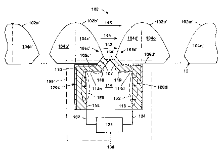
Referring now to Fig. 2, a radiator element 100 which is similar to the
radiator
element formed by fin-shaped members 16a, 16b of FIG. 1, is one of a plurality
of radiators
elements 100 forming an antenna array according to the invention. The radiator
element 100
which forms one-half of a unit cell, similar to the unit cell 14 (FIG. 1),
includes a pair of
substrates 104c and 104d (generally referred to as substrates 104) which are
provided by
CA 02527642 2005-11-29
WO 2005/015687 PCT/US2004/016336
separate fins 102b and 102c respectively. It should be noted that substrates
104c, 104d
correspond to the fin-shaped members 16a, 16b (or 18a, 18b) of FIG. 1 while
fins 102a, 102b
correspond to the back-to-back fin-shaped elements discussed above in
conjunction with
FIG. 1. The fins 102b and 102c are disposed on the cavity plate 12 (FIG. 1).
Fin 102b also
5 includes substrate 104b which forms another radiator element in conjunction
with substrate
104a of fin 102a. Each substrate 104c and 104d has a planar feed which
includes a feed
surface 106c and 106d and a transition section 105c and 105d (generally
referred to as
transition sections 105), respectively. The radiator element 100 further
includes a balanced
symmetrical feed circuit 108 (also referred to as balanced symmetrical feed
108) which is
10 electromagnetically coupled to the transition sections 105.
The balanced symmetrical feed 108 includes a dielectric 110 having a cavity
116
with the dielectric having internal surfaces 118a and external surfaces 118b.
A metalization
layer 114c is disposed on the internal surface 118a and a metalization layer
120c is disposed
on the external surface 118b. In a similar manner, a metalization layer 114d
is disposed on
the internal surface 118a and a metalization layer 120d is disposed on the
external surface
118b. It should be appreciated by one of skill in the art that the
metalization layer 114c (also
referred to as feed line or RF feed line 114c) and the metalization layer 120c
(also referred to
as ground plane 120c) interact as microstrip circuitry 140a wherein the ground
plane 120c
provides the ground circuitry and the feed line 114c provides the signal
circuitry for the
microstrip circuitry 140a. Furthermore, the metalization layer 114d (also
referred to as feed
line or RF feed line 114d) and the metalization layer 120d (also referred to
as ground plane
120d) interact as microstrip circuitry 140b wherein the ground plane 120d
provides the
ground circuitry and the feed line 114d provides the signal circuitry for the
microstrip
circuitry 140b.
The balanced symmetrical feed 108 further includes a balanced-unbalanced
(balun)
feed 136 having an RF signal line 138 and first RF signal output line 132 and
a second RF
signal output line 134. The first RF signal output line 132 is coupled to the
feed line 114c
and the second RF signal output line 134 is coupled to the feed line 114d. It
should be
appreciated two 180 baluns 136 are required for the unit cell similar to unit
cell 14, one
balun to feed the radiator elements for each polarization. Only one balun 136
is shown for
clarity. The baluns 136 are required for proper operation of the radiator
element 100 and
provide simultaneous dual polarized signals at the output ports with
relatively good isolation.
The baluns 136 can be provided as part of the balanced symmetrical feed 108 or
as separate
CA 02527642 2005-11-29
WO 2005/015687 PCT/US2004/016336
11
components, depending on the power handling and mission requirements. A first
signal
output of the balun 136 is connected to the feed line 114c and the second RF
signal output of
the balun 136 is connected to the feed line 114d, and the signals propagate
along the
microstrip circuitry 140a and 140b, respectively, and meet at signal null
point 154 with a
phase relationship 180 degrees out of phase as described further herein after.
It should be
noted that substrate 104c includes a feed surface 106c and substrate 104d
includes a feed
surface 106d that is diposed along metalization layer 120c and 120d,
respectively.
The radiator element 100 provides a co-located (coincident) radiation pattern
phase
center for each polarization signal being transmitted or received. The
radiator element 100
provides cross polarization isolation levels in the principal plane and in the
diagonal planes
to allow scanning beams out to 60 .
In operation, RF signals are fed differentially from the balun 136 to the
signal
output line 132 and the signal output line 134, here at a phase difference of
180 degrees.
The RF signals are coupled to microstrip circuitry 140a and 140b, respectively
and
propagate along the microstrip circuitry meeting at signal null point 154 at a
phase
difference of 180 degrees where the signals are destructively combined to zero
at the feed
point. The RF signals propagating along the microstrip circuitry 140a and 140b
are
coupled to the slot 141 and radiate or "are launched" from transition sections
105c and
105d. These signals form a beam, the boresight of which is orthogonal to the
cavity plate
12 in the direction away from the cavity 116. The RF signal line 138 is
coupled to
receive and transmit circuits as is know in the art using a circulator (not
shown) or a
transmit/receive switch (not shown).
Field lines 142, 144, 146 illustrate the electric field geometry for radiator
element
100. In the region around metalization layer 120c, the electric field lines
150 extend
from the metalization layer 120c to the feed line 114c. In the region around
metalization
layer 120d the electric field lines 152 extend from the feed line 114d to the
metalization
layer 120d. In the region around feed surface 106c, the electric field lines
148 extend
from the metalization layer 120c to the feed line 114c. In the region around
feed surface
106d, the electric field lines 149 extend from the feed line 114d to the
metalization layer
120d. At a field point 154 (also referred to as a signal null point 154), the
electric field
lines 148 and 149 from the feed lines 114c and 114d substantially cancel each
other
forming the signal null point 154. The arrangement of feed lines 114c and 114d
and
transition sections 105c and 105d reduce the excitation of asymmetric modes
which
CA 02527642 2005-11-29
WO 2005/015687 PCT/US2004/016336
12
increase loss mismatch and cross polarization. Here, the launched TEM modes
shown as
electric field lines 142 are transformed through intermediate electric field
lines 144
having Floquet modes shown as field lines 146. Received signals initially
having Floquet
modes collapse into balanced TEM modes.
The pair of substrates 104c and 104d and corresponding transition sections
105c
and 105d can be thought of as two halves making up a dipole. Thus, the signals
on feed
lines 114c and 114d will ordinarily be 180 out of phase. Likewise, the
signals on each of
the feed lines of the orthogonal transitions (not shown) forming the unit cell
similar to the
unit cell 14 (FIG. 1) will be 180 out of phase. As in a conventional dipole
array, the
relative phase of the signals at the transition sections 105c and 105d will
determine the
polarization of the signals transmitted by the radiator element 100.
In an alternative embodiment, the metalization layer 120c and 120d along the
feed
surface 106c and 106d, respectively, can be omitted with the metalization
layer 120c
connected to the feed surface 106c where they intersect and the metalization
layer 120d
connected to the surface 106d where they intersect. In this alternative
embodiment, the
feed surface 106c and 106d provide the ground layer for the microstrip
circuitry 140a and
140b, respectively along the bottom of the substrate 104c and 104d,
respectively.
In another alternate embodiment, amplifiers (not shown) are coupled between
the
balun 136 signal output lines 132 and 134 and the transmission feeds 114c and
114d
respectively. In this alternate embodiment, most of the losses associated with
the balun
136 are behind the amplifiers.
Referring now to FIGs. 3 and 3A in which like elements in FIGs. 2, 3 and 3A
are
provided having like reference designations, a radiator element 100' (also
referred to as
an electrically short crossed notch radiator element 100') includes a pair of
substrates
104c' and 104d' (generally referred to as substrates 104'). It should be noted
that
substrates 104c', 104d' correspond to the fin-shaped members 16a, 16b (or 18a,
18b) of
FIG. 1. Each substrate 104c' and 104d' has a pyramidal feed which includes a
feed
surface 106c' and 106d' and a transition section 105c' and 105d' (generally
referred to as
transition sections 105') respectively. The transition sections 105' and feed
surfaces 106'
differ from the corresponding transition sections 105 and feed surfaces 106 of
FIG. 2 in
that the transition sections 105' and feed surfaces 106' include notched ends
107 forming
an arch. The feed surfaces 106c' and 106d' are coupled with a similarly shaped
balanced
symmetrical feed 108' (also referred to as a raised balanced symmetrical
feed).
CA 02527642 2005-11-29
WO 2005/015687 PCT/US2004/016336
13
The transition section 105' has improved impedance transfer into space. It
will be
appreciated by those of ordinary skill in the art, the transition sections
105' can have an
arbitrary shape, for example, the arch formed by notched ends 107 can be
shaped
differently to affect the transfer impedance to provide a better impedance
match. The
taper of the transition sections 105' can be adjusted using known methods to
match the
impedance of the fifty ohm feed to free space.
More specifically, the balanced symmetrical feed 108' includes a dielectric
110
having a cavity 116 with the dielectric having internal surfaces 118a and
external
surfaces 118b. A metalization layer 114c is disposed on the internal surface
118a and a
metalization layer 120c is disposed on the external surface 118b. In a similar
manner, a
metalization layer 114d is disposed on the internal surface 118a and a
metalization layer
120d is disposed on the external surface I I8b. It should be appreciated by
one of skill in
the art that the RF feed line 114c and the metalization layer 120c (also
referred to as
ground plane 120c) interact as microstrip circuitry 140a wherein the ground
plane 120c
provides the ground circuitry and the feed line 114c provides the signal
circuitry for the
microstrip circuitry 140a. Furthermore, the or RF feed line l 14d and the
metalization
layer 120c (also referred to as ground plane 120d) interact as microstrip
circuitry 140b
wherein the ground plane 120d provides the ground circuitry and the feed line
114d
provides the signal circuitry for the microstrip circuitry 140b.
The balanced symmetrical feed 108' further includes a balun 136 similar to
balun
136 of FIG.2. A first signal output of the balun 136 is connected to the feed
line 114c
and the second RF signal output of the balun 136 is connected to the feed line
114d
wherein the signals propagate along the microstrip circuitry 140a and 140b,
respectively,
and meet at signal null point 154' with a phase relationship 180 degrees out
of phase.
Again, it should be noted that substrate 104c includes a feed surface 106c and
substrate
104d includes a feed surface 106d that is diposed along metalization layer
120c and 120d,
respectively. The radiator element 100' provides a co-located (coincident)
radiation
pattern phase center for each polarization signal being transmitted or
received. The
radiator element 100 provides cross polarization isolation levels in the
principal plane and
in the diagonal planes to allow scanning beams approaching 60 .
In operation, RF signals are fed differentially from the balun 136 to the
signal
output line 132 and the signal output 134, here at a phase difference of 180
degrees. The
signals are coupled to microstrip circuitry 140a and 140b, respectively and
propagate
CA 02527642 2005-11-29
WO 2005/015687 PCT/US2004/016336
14
along the microstrip circuitry meeting at signal null point 154' at a phase
difference of
180 degrees where the signals are destructively combined to zero at the feed
point. The
RF signals propagating along the microstrip circuitry 140a and 140b are
coupled to the
slot 141 and radiate or "are launched" from transition sections 105c' and
105d'. These
signals form a beam, the boresight of which is orthogonal to the cavity plate
12 in the
direction away from cavity 116. The RF signal line 138 is coupled to receive
and
transmit circuits as is known in the art using a circulator (not shown) or a
transmit/receive
switch (not shown).
Field lines 142, 144, 146 illustrate the electric field geometry for radiator
element
100'. In the region around metalization layer 120c, the electric field lines
150 extend from
the metalization layer 120c to the feed line 114c. In the region around
metalization layer
120d the electric field lines 152 extend from the feed line 114d to the
metalization layer
120d. In the region around feed surface 106c', the electric field lines 148
extend from the
metalization layer 120c to the feed line 114c. In the region around feed
surface 106d', the
electric field lines 149 extend from the feed line 114d to the metalization
layer 120d. At a
signal null point 154', the RF field lines from the RF feed lines 114c and
114d substantially
cancel each other forming a signal null point 154'. The arrangement of RF feed
lines 114c
and 114d and transition sections 105c' and 105d' reduce the excitation of
asymmetric modes
which increase loss mismatch and cross polarization. Here, the launched TEM
modes shown
as electric field lines 142 are transformed through intermediate electric
field lines 144 having
Floquet modes shown as field lines 146. Received signals initially having
Floquet modes
collapse into balanced TEM modes.
In one embodiment the radiator element 100' includes fins 102b' and 102c'
(generally referred to as fins 102') having heights of less than 0.25a,L,
where XL refers to
the wavelength of the low end of a range of operating wavelengths. Although in
theory,
radiator elements this short should stop radiating or have degraded
performance, it was
found the shorter elements actually provided better performance. The fins
102b' and
102c' are provided with a shape which matches the impedance of the balanced
symmetrical feed 108' circuit to free space. The shape can be determined
empirically or
by mathematical techniques known in the art. The electrically short crossed
notch
radiator element 100' includes portions of two pairs of metal fins 102b' and
102c'
disposed over an open cavity 116 provided by the balanced symmetrical feed
108'. Each
CA 02527642 2005-11-29
WO 2005/015687 PCT/US2004/016336
pair of metal fins 102' is disposed orthogonal to the other pair of metal fins
(not shown).
In one embodiment, the cavity 116 wall thickness is 0.030 inches. This wall
thickness provides sufficient strength to the array structure and is the same
width as the
radiator fins 102' used in the aperture. Radiator fin 102' length, measured
from the feed
5 point in the throat of the crossed fins 102' to the top of the fin is 0.250
inches without a
radome (not shown) and operating at a frequency of 7 - 21 GHz. The length may
possibly
be even shorter with a radome/matching structure (e.g. matching sheet 30 in
FIG. 1).. It
should be appreciated the impedance characteristics of the radome affect the
signal
transition into free space and could enable shorter fins 102'. It will be
appreciated by
10 those of ordinary skill in the art that the cavity 116 wall dimensions and
the fin 102'
dimensions can be adjusted for different operating frequency ranges.
The theory of operation behind the electrically short crossed notch radiator
element 100' is based on the Marchand Junction Principle. The original
Marchand balun
was designed as a coax to balanced transmission line converter. The Marchand
balun
15 converts the signal from an unbalanced TEM mode on a first end of the
coaxial line to a
balanced mode on a second end. The conversion takes place at a virtual
junction where
the fields in one mode (TEM) collapse and go to zero and are reformed on the
other side
as the balanced mode with very little loss due to the conservation of energy.
Mode field
cancellation occurs when the RF field on the transmission line is split into
two signals,
180 degrees out-of-phase from each other and then combined together at a
virtual
junction. This is accomplished by splitting the signal at a junction
equidistant from two
opposing boundary conditions, such as open and short circuits. For the
electrically short
crossed notch radiator element 100', the input for one polarization is a pair
of microstrip
lines provided by feed surfaces 106' and notched ends 107 (operating in TEM
mode)
which feed one side with a zero degree signal and the other side with a 180
degrees out-
of-phase signal. These signals come together at a virtual junction signal null
point 154',
also referred to as the throat of the electrically short crossed notch
radiator element 100'.
At the signal null point 154', the fields collapse and go to zero and are
reformed
on the other side in the balanced slotline of the electrically short crossed
notch radiator
element 100' and propagate outward to free space. The two opposing boundary
conditions for the electrically short crossed notch radiator element 100' are
the shorted
cavity beneath the element 100' and the open circuit formed at the tip
(disposed near
electric field lines 146) of each pair of the radiator fins 102b' and 102c'.
The operation of
CA 02527642 2005-11-29
WO 2005/015687 PCT/US2004/016336
16
the virtual junction is reciprocal for both transmit and receive.
In one embodiment the short radiating fins and cavity are molded as a single
unit
to provide close tolerances at the gap where the four crossed fins 102' meet.
The balanced
symmetrical feed circuit 108' can also be molded to fit into the cavity area
below the fins
102' further simplifing the assembly. For receive applications balun circuits
136 are
included in the balanced symmetrical feed circuit 108' further reducing the
profile for the
array. The short crossed notch radiator element 100' represents a significant
advance
over conventional wideband notch radiators by providing broad bandwidth in a
relatively
smaller profile using printed cirucit board technology and relatively short
radiator
elements 100'. The radiator elements 100' use co-located (coincident)
radiation pattern
phase centers which are advantageous for certain applications and the
physically
relatively short profile. Other wideband notch radiators, including the more
complex
quad notch radiator, do not have the wide angle diagonal plane cross-
polarization
isolation characteristics of the electrically short crossed notch radiator
element 100'. The
combination of the balanced symmetrical feed circuit 108' and the short fins
102'
provides a reactively coupled notch antenna. The reactively coupled notch
enables the
use of shorter fin lengths, thereby improving the cross-pol isolation. The
length of the
fins 102' directly impacts the wideband performance and the cross-polarization
isolation
levels acheived.
In another embodiment, the fins 102' are much (previous discussion page 15
line
6 had less than... guess this should be much shorter) shorter than
approximately 0.25XL,
where ?L refers to the wavelength of the low end of a range of operating
wavelengths and
the broadband dual polarized electrically short crossed notch antenna radiator
element
100' transmits and receives signals with selective polarization with co-
located
(coincident) radiation pattern phase centers having excellent cross-
polarization isolation
and axial ratio in the principal and diagonal planes. When coupled with the
inventive
balanced symmetrical feed arrangement, the radiator element 100' provides a
low profile
and broad bandwidth. In this embodiment, short fins 102' also provide a
reactively
coupled notch antenna. The length of the prior art fins was determined to be
the main
source of the poor cross-polarization isolation performance in the diagonal
planes. It was
determined that both the diagonal plane co-polarization and diagonal plane
cross-
polarization levels varied as a function of the electrical length of the fin.
A further
CA 02527642 2005-11-29
WO 2005/015687 PCT/US2004/016336
17
advantage of the electrically short crossed notch radiator fins used in an
array
environment is the high cross polarization isolation levels achieved in the
diagonal planes
out past fifty degrees of scan as compared to current notch radiator designs
which can
scan out to only twenty degrees.
Referring now to FIG. 4, a unit cell 202 includes a plurality of fin-shaped
elements 204a, 204b disposed over a balanced symmetrical pyramidal feed
circuit 220.
Each pair of radiator elements 204a and 204b is centered over the balanced
symmetrical
feed 220 which is disposed in an aperture (not visible in Fig. 4) formed in
the cavity plate
12 (FIG. 1). The first one of the pair of radiator elements 204a is
substantially orthogonal
to the second one of the pair of radiator elements 204b. It should be
appreciated that no
RF connectors are required to couple the signal from to the balanced
symmetrical feed
circuit 220. The unit cell 202 is disposed above the balanced symmetrical feed
220
which provides a single open cavity. The inside of the cavity walls are
denoted as 228.
Referring to FIG. 4A, the exemplary balanced symmetrical feed 220 of the unit
cell 202 includes a housing 226 having a center feed point 234 and feed
portions 232a
and 232b corresponding to one polarization of the unit cell and feed portions
236a and
236b corresponding to the orthogonal polarization of the unit cell. The
housing 226
further includes four sidewalls 228. Each of the feed portions 232a and 232b
and 236a
and 236b have an inner surface and includes a microstrip feed line (also
referred to as RF
feed line) 240 and 238 which are disposed on the respective inner surfaces.
Each
microstrip feed line 240 and 238 is further disposed on the inner surfaces of
the
respective sidewalls 228. The microstrip feed lines 238 and 240 cross under
each
corresponding fin-shaped substrate 204a, 204b and join together at the center
feed point
234. The center feed point 234 of the unit cell is raised above an upper
portion of the
sidewalls 228 of the housing 226. The housing 226, the sidewalls 228 and the
cavity
plate 212 provide the cavity 242. The microstrip feed lines 240 and 238 cross
at the
center feed point 234, and exit at the bottom along each wall of the cavity
242. As shown
a microstrip feed 244b, formed where the metalization layer on sidewall 228 is
removed,
couples the RF signal to the aperture 222 in the cavity plate 212. In the unit
cell 202, a
junction is formed at the center feed point 234 and according to Kirchoff's
node theory
the voltage at the center feed point 234 will be zero.
CA 02527642 2005-11-29
WO 2005/015687 PCT/US2004/016336
18
In one particular embodiment, the balanced symmetrical feed 220 is a molded
assembly that conforms to the feed surface of the substrate of the fins 204a
and 204b. In
this particular embodiment, the microstrip feed lines 240 and 238 are formed
by etching
the inner surface of the assembly. In this particular embodiment, the housing
226 and
the feed portions 232 and 236 molded dielectrics. In this embodiment, the
radiator height
is 0.250 inches, the balanced symmetrical feed 220 is square shaped with each
side
measuring 0.285 inches and having a height of 0.15 inches. The corresponding
lattice
spacing is 0.285 inches for use at a frequency of 7 - 21 GHz. At the center
feed point 234,
a 0.074 inch square patch of ground plane material is removed to allow the RF
fields on
the microstrip feed lines 240 and 238 to propagate up the radiator elements
204 and
radiate out the aperture. In order to radiate properly the microstrip feed
lines 240 and 238
for each polarization are fed 180 degrees out-of-phase so when the two
opposing signals
meet at the center feed point 234 the signals cancel on the microstrip feed
lines 240 and
238 but the energy on the microstrip feed lines 240 and 238 is transferred to
the radiator
elements 204a and 204b to radiate outward. For receive signals, the opposite
occurs
where the signal is directed down the radiator elements 204a and 204b and is
imparted
onto the microstrip feed lines 240 and 238 and split into two signals 180
degrees out-of-
phase. In another embodiment, the balun (not shown) is incorporated into the
balanced
symmetrical feed 220.
Referring now to FIG. 5, a curve 272 represents the swept gain of a prior art
center radiator element at zero degrees boresight angle versus frequency.
Curve 270
represents the maximum theoretical gain for a radiator element and curve 274
represents
a curve 6 db or more below the gain curve 270. Resonances present in the prior
art
radiator result in reduction in antenna gain as indicated in curve 272.
Referring now to FIG. 5A, a curve 282 represents the measured swept gain of
the
concentrically fed electrically short crossed notch radiator element 100' of
FIG. 3 at zero
degrees boresight angle versus frequency. Curve 280 represents the maximum
theoretical
gain for a radiator element and curve 284 represents a curve approximately 1 -
3 db below
the gain curve 280. The curve has a measurement artifact at point 286 and a
spike at
point 288 due to grating lobes. Comparing curves 272 and 282, it can be seen
that there
is a difference of approximately 6 dB (4 times in power) between the gain of
the
electrically short crossed notch radiator element 100' compared to the prior
art radiator
element. Therefore, approximately four times as many prior art radiator
elements (or
CA 02527642 2005-11-29
WO 2005/015687 PCT/US2004/016336
19
equivalently four times the aperture size of an array of prior art radiators)
would be
required to provide the performance of one of the electrically short crossed
notch radiator
element 100' of FIG. 3 over a 9:1 bandwidth range. Because of the performance
of the
electrically short crossed notch radiator element 100', the element 100' can
operate as an
allpass device.
When fed by a balun approaching ideal performance, the electrically short
crossed
notch radiator element 100' can be considered as a 4-port device, one
polarization is
generated with ports one and two being fed at uniform magnitude and a 180
phase
relationship. Ports three and four excited similarly will generate the
orthogonal
polarization. From two through eighteen GHz, the mismatch loss is
approximately 0.5
dB or less over the cited frequency range and 60 conical scan volume. The
impedance
match also remains well controlled over most of the H-plane scan volume.
Referring now to Fig. 6, a set of curves 292-3 10 illustrate the polarization
purity
of the electrically short crossed notch radiator element 100' (FIG. 3). The
curves are
generated for a single antenna element of the type shown in the array of FIG.
I embedded
in the center of an array with all other radiators terminated.
An embedded element pattern is the element pattern in the array environment
that
includes the mutual coupling effects. The embedded element pattern taken on a
mutual
coupling array (MCA) was measured. The data shown was taken on the center
element
of this array near mid band.
Patterns are given for the co-polarized and cross-polarized performance for
the
various planes (E, H, and diagonal (D)). As can be seen from the curves 292-3
10, the
antenna is provided having better than 10 dB cross-polarization isolation over
a 60
conical scan volume. Curves 292, 310 illustrate the co-polarized and cross-
polarized
patterns of the center element in the electrical plane (E), respectively.
Curves 249 and
300 illustrate the co-polarized and cross-polarized patterns of the center
element in the
magnetic plane (H), respectively. Curves 290 and 296 illustrate the co-
polarized and
cross-polarized patterns of the center element in the diagonal plane,
respectively. Curves
292, 310, 249, 300, 290, and 296 illustrate that the electrically short
crossed notch
radiator element 100' exhibits good cross-polarization isolation performance.
In an alternate embodiment, an assembly of two sub components, the fins 102
and
102'and the balanced symmetrical feed circuits 108 and 108' of FIGs. 1 and 3
respectively, are provided as monolithic components to guarantee accurate
alignment of
CA 02527642 2011-10-14
78625-30
the fins with each other and equal gap spacing at the feed point. By keeping
tolerances at
a minimum and unit-to-unit uniformity, consistent performance over scan angles
and
frequency can be achieved.
In a further embodiment, the fin components of the radiator elements 100 and
5 100' can be machined, cast, or injection molded to forma single assembly.
For example,
a metal matrix composite such as AISiC can provide a very lightweight, high
strength
element with a low coefficient of thermal expansion and high thermal
conductivity.
In another alternate embodiment, radiator elements 100 and 100' are protected
from the surrounding environment by a radome (not shown) disposed over the
radiating
10 elements in the array. The radome can be an integral part of the antenna
and used as part
of the wideband impedance matching process as a single wide angle impedance
matching
sheet or an A sandwich type radome can be used as is known in the art.
15 Having described the preferred embodiments of the invention, it will now
become
apparent to one of ordinary skill in the art that other embodiments
incorporating their
concepts may be used. It is felt therefore that these embodiments should not
be limited to
disclosed embodiments but rather should be limited only by the spirit and
scope of the
appended claims.
What is claimed is: