Sélection de la langue

Search

Sommaire du brevet 2528128 

Énoncé de désistement de responsabilité concernant l'information provenant de tiers

Une partie des informations de ce site Web a été fournie par des sources externes. Le gouvernement du Canada n'assume aucune responsabilité concernant la précision, l'actualité ou la fiabilité des informations fournies par les sources externes. Les utilisateurs qui désirent employer cette information devraient consulter directement la source des informations. Le contenu fourni par les sources externes n'est pas assujetti aux exigences sur les langues officielles, la protection des renseignements personnels et l'accessibilité.

Disponibilité de l'Abrégé et des Revendications

L'apparition de différences dans le texte et l'image des Revendications et de l'Abrégé dépend du moment auquel le document est publié. Les textes des Revendications et de l'Abrégé sont affichés :

  • lorsque la demande peut être examinée par le public;
  • lorsque le brevet est émis (délivrance).
(12) Demande de brevet: (11) CA 2528128
(54) Titre français: REGLAGE DES CARACTERISTIQUES DE PHASE ET D'AMPLITUDE DE SIGNAUX DE COMMUNICATION SANS FIL GENERES PAR EMETTEUR, EN REPONSE A DES SIGNAUX DE COMMANDE DE PUISSANCE D'EMISSION DE STATION DE BASE ET DE CARACTERISTIQUES D'AMPLIFICATEURS CONNUES
(54) Titre anglais: ADJUSTING THE AMPLITUDE AND PHASE CHARACTERISTICS OF TRANSMITTER GENERATED WIRELESS COMMUNICATION SIGNALS, IN RESPONSE TO BASE STATION TRANSMIT POWER CONTROL SIGNALS AND KNOWN TRANSMITTER AMPLIFIER CHARACTERISTICS
Statut: Réputée abandonnée et au-delà du délai pour le rétablissement - en attente de la réponse à l’avis de communication rejetée
Données bibliographiques
(51) Classification internationale des brevets (CIB):
  • H04K 01/02 (2006.01)
(72) Inventeurs :
  • DEMIR, ALPASLAN (Etats-Unis d'Amérique)
  • KAZAKEVICH, LEONID (Etats-Unis d'Amérique)
  • NARAYAN, GEETHA LAKSHMI (Etats-Unis d'Amérique)
(73) Titulaires :
  • INTERDIGITAL TECHNOLOGY CORPORATION
(71) Demandeurs :
  • INTERDIGITAL TECHNOLOGY CORPORATION (Etats-Unis d'Amérique)
(74) Agent: SMART & BIGGAR LP
(74) Co-agent:
(45) Délivré:
(86) Date de dépôt PCT: 2004-05-06
(87) Mise à la disponibilité du public: 2005-01-06
Requête d'examen: 2005-12-05
Licence disponible: S.O.
Cédé au domaine public: S.O.
(25) Langue des documents déposés: Anglais

Traité de coopération en matière de brevets (PCT): Oui
(86) Numéro de la demande PCT: PCT/US2004/013906
(87) Numéro de publication internationale PCT: US2004013906
(85) Entrée nationale: 2005-12-05

(30) Données de priorité de la demande:
Numéro de la demande Pays / territoire Date
10/749,025 (Etats-Unis d'Amérique) 2003-12-30
60/476,315 (Etats-Unis d'Amérique) 2003-06-06

Abrégés

Abrégé français

La présente invention concerne un procédé est un système de réglage des caractéristiques d'amplitude et de phase de signaux de communication sans fil générés par un émetteur radio analogique, à partir de signaux de commandes de puissance d'émission (TPC) reçus par une station de base (BS) et de caractéristiques d'un amplificateur de puissance (PA) inclus dans l'émetteur. Un module de compensation de pré-distorsion numérique, possédant des trajets de signal réel et imaginaire, reçoit et traite des composants de signal réel et imaginaire utilisés pour générer le signal de communication sans fil. Des caractéristiques de phrase et d'amplitude du signal de communication sans fil sont commandés en réponse aux signaux TPC, de façon que des caractéristiques d'amplitude et de phase erronées de l'amplificateur PA soient corrigées.


Abrégé anglais


A method and system for adjusting the amplitude and phase characteristics of
wireless communication signals generated by an analog radio transmitter, based
on transmit power control (TPC) signals received by a base station (BS) and
known characteristics of a power amplifier (PA) included in the transmitter. A
digital pre-distortion compensation module, having real and imaginary signal
paths, receives and processes real and imaginary signal components used to
generate the wireless communication signal. The phase and amplitude
characteristics of the wireless communication signal are controlled in
response to the TPC signals, such that impaired amplitude and phase
characteristics of the PA are corrected.

Revendications

Note : Les revendications sont présentées dans la langue officielle dans laquelle elles ont été soumises.


CLAIMS
What is claimed is:
1. A digital baseband (DBB) transmitter for transmitting at least one
wireless communication signal to a base station (BS) which is configured to
generate a transmit power control (TPC) signal in response to receiving the
wireless communication signal, the DBB transmitter comprising:
(a) a digital pre-distortion compensation module having real and
imaginary signal paths which are configured to receive and process respective
real and imaginary signal components used to generate the wireless
communication signal;
(b) an analog radio transmitter including a power amplifier (PA), the
analog radio transmitter being configured to receive the processed real and
imaginary signal components and, in response, generating a communication
signal which is input to the PA, the PA being configured to amplify the
generated
communication signal, wherein the amplified communication signal is emitted
from the DBB transmitter as the wireless communication signal;
(c) a controller in communication with the digital pre-distortion
compensation module and the PA, the controller being configured to control the
characteristics of the wireless communication signal based on the TPC signal
generated by the BS;
(d) a modem having real and imaginary signal paths and being configured
to generate the real and imaginary signal components, receive the TPC signal
and to pass the TPC signal to the controller;
(e) a first low pass filter (LPF) which couples the real signal path of the
modem to the real signal path of the digital pre-distortion compensation
module;
and
(f) a second LPF which couples the imaginary signal path of the modem to
the imaginary signal path of the digital pre-distortion compensation module.
-13-

2. The DBB transmitter of claim 1 wherein the controller includes a
TPC mapping unit which receives the TPC signal from the modem, the TPC
mapping unit being configured to output a first mapped TPC signal to the
digital
pre-distortion compensation module and a second mapped TPC signal to the PA.
3. The DBB transmitter of claim 2 wherein the digital pre-distortion
compensation module comprises:
(i) a power estimation unit coupled to each of the real and imaginary signal
paths, the power estimation unit being configured to generate a power
estimation
signal based on the magnitude of the real and imaginary signal components;
(ii) a first multiplier being configured to multiply the power estimation
signal with the first mapped TPC signal to generate a first resulting product
signal;
(iii) at least one look up table (LUT) being configured to generate an
amplitude compensation signal in response to receiving the first resulting
product signal; and
(iv) a phase distortion compensation unit being configured to generate a
phase compensation signal in response to receiving the first resulting product
signal.
4. The DBB transmitter of claim 3 wherein the digital pre-distortion
compensation module further comprises:
(v) a second multiplier being configured to multiply the amplitude
compensation signal with the real signal component to generate a second
resulting product signal;
(vi) a first adder being configured to add the second resulting product
signal to the real signal component to generate an amplitude compensated real
signal component;
(vii) a third multiplier being configured to multiply the amplitude
compensation signal with the imaginary signal component to generate a third
resulting product signal; and
-14-

(viii) a second adder being configured to add the third resulting product
signal to the imaginary signal component to generate an amplitude compensated
imaginary signal component.
5. The DBB transmitter of claim 4 wherein the digital pre-distortion
compensation module further comprises:
(ix) a fourth multiplier being configured to multiply the phase
compensation signal with the amplitude compensated real signal component to
generate a fourth resulting product signal;
(x) a third adder being configured to add the fourth resulting product
signal to the amplitude compensated imaginary signal component;
(xi) a fifth multiplier being configured to multiply the phase compensation
signal with the amplitude compensated imaginary signal component to generate
a fifth resulting product signal; and
(xii) a fourth adder being configured to subtract the fifth resulting product
signal from the amplitude compensated real signal component.
6. The DBB transmitter of claim 5 wherein the amplitude
compensation signal is used by the digital pre-distortion compensation module
to
correct at least one impaired amplitude characteristic associated with the PA.
7. The DBB transmitter of claim 3 wherein the phase compensation
signal is used by the digital pre-distortion compensation module to correct at
least one impaired phase characteristic associated with the PA.
8. The DBB transmitter of claim 2 wherein the second mapped TPC
signal is used to adjust the gain of the PA such that the PA does not operate
in a
nonlinear fashion.
9. A wireless transmit/receive unit (WTRU) for transmitting at least
one wireless communication signal to a base station (BS) which is configured
to
-15-

generate a transmit power control (TPC) signal in response to receiving the
wireless communication signal, the WTRU comprising:
(a) a digital pre-distortion compensation module having real and
imaginary signal paths which are configured to receive and process respective
real and imaginary signal components used to generate the wireless
communication signal;
(b) an analog radio transmitter including a power amplifier (PA), the
analog radio transmitter being configured to receive the processed real and
imaginary signal components and, in response, generating a communication
signal which is input to the PA, the PA being configured to amplify the
generated
communication signal, wherein the amplified communication signal is emitted
from the WTRU as the wireless communication signal;
(c) a controller in communication with the digital pre-distortion
compensation module and the PA, the controller being configured to control the
characteristics of the wireless communication signal based on the TPC signal
generated by the BS;
(d) a modem having real and imaginary signal paths and being configured
to generate the real and imaginary signal components, receive the TPC signal
and to pass the TPC signal to the controller;
(e) a first low pass filter (LPF) which couples the real signal path of the
modem to the real signal path of the digital pre-distortion compensation
module;
and
(f) a second LPF which couples the imaginary signal path of the modem to
the imaginary signal path of the digital pre-distortion compensation module.
10. The WTRU of claim 9 wherein the controller includes a TPC
mapping unit which receives the TPC signal from the modem, the TPC mapping
unit being configured to output a first mapped TPC signal to the digital pre-
distortion compensation module and a second mapped TPC signal to the PA.
-16-

11. The WTRU of claim 10 wherein the digital pre-distortion
compensation module comprises:
(i) a power estimation unit coupled to each of the real and imaginary signal
paths, the power estimation unit being configured to generate a power
estimation
signal based on the magnitude of the real and imaginary signal components;
(ii) a first multiplier being configured to multiply the power estimation
signal with the first mapped TPC signal to generate a first resulting product
signal;
(iii) at least one look up table (LUT) being configured to generate an
amplitude compensation signal in response to receiving the first resulting
product signal; and
(iv) a phase distortion compensation unit being configured to generate a
phase compensation signal in response to receiving the first resulting product
signal.
12. The WTRU of claim 11 wherein the digital pre-distortion
compensation module further comprises:
(v) a second multiplier being configured to multiply the amplitude
compensation signal with the real signal component to generate a second
resulting product signal;
(vi) a first adder being configured to add the second resulting product
signal to the real signal component to generate an amplitude compensated real
signal component;
(vii) a third multiplier being configured to multiply the amplitude
compensation signal with the imaginary signal component to generate a third
resulting product signal; and
(viii) a second adder being configured to add the third resulting product
signal to the imaginary signal component to generate an amplitude compensated
imaginary signal component.
-17-

13. The WTRU of claim 14 wherein the digital pre-distortion
compensation module further comprises:
(ix) a fourth multiplier being configured to multiply the phase
compensation signal with the amplitude compensated real signal component to
generate a fourth resulting product signal;
(x) a third adder being configured to add the fourth resulting product
signal to the amplitude compensated imaginary signal component;
(xi) a fifth multiplier being configured to multiply the phase compensation
signal with the amplitude compensated imaginary signal component to generate
a fifth resulting product signal; and
(xii) a fourth adder being configured to subtract the fifth resulting product
signal from the amplitude compensated real signal component.
14. The WTRU of claim 11 wherein the amplitude compensation signal
is used to correct at least one impaired amplitude characteristic associated
with
the PA.
15. The WTRU of claim 11 wherein the phase compensation signal is
used to correct at least one impaired phase characteristic associated with the
PA.
16. The WTRU of claim 10 wherein the second mapped TPC signal is
used to adjust the gain of the PA such that the PA does not operate in a
nonlinear
fashion.
17. An integrated circuit (IC) for transmitting at least one wireless
communication signal to a base station (BS) which is configured to generate a
transmit power control (TPC) signal in response to receiving the wireless
communication signal, the IC comprising:
(a) a digital pre-distortion compensation module having real and
imaginary signal paths which are configured to receive and process respective
-18-

real and imaginary signal components used to generate the wireless
communication signal;
(b) an analog radio transmitter including a power amplifier (PA), the
analog radio transmitter being configured to receive the processed real and
imaginary signal components and, in response, generating a communication
signal which is input to the PA, the PA being configured to amplify the
generated
communication signal, wherein the amplified communication signal is emitted
from the IC as the wireless communication signal;
(c) a controller in communication with the digital pre-distortion
compensation module and the PA, the controller being configured to control the
characteristics of the wireless communication signal based on the TPC signal
generated by the BS;
(d) a modem having real and imaginary signal paths and being configured
to generate the real and imaginary signal components, receive the TPC signal
and to pass the TPC signal to the controller;
(e) a first low pass filter (LPF) which couples the real signal path of the
modem to the real signal path of the digital pre-distortion compensation
module;
and
(f) a second LPF which couples the imaginary signal path of the modem to
the imaginary signal path of the digital pre-distortion compensation module.
18. The IC of claim 17 wherein the controller includes a TPC mapping
unit which receives the TPC signal from the modem, the TPC mapping unit being
configured to output a first mapped TPC signal to the digital pre-distortion
compensation module and a second mapped TPC signal to the PA.
19. The IC of claim 18 wherein the digital pre-distortion compensation
module comprises:
(i) a power estimation unit coupled to each of the real and imaginary signal
paths, the power estimation unit being configured to generate a power
estimation
signal based on the magnitude of the real and imaginary signal components;
-19-

(ii) a first multiplier being configured to multiply the power estimation
signal with the first mapped TPC signal to generate a first resulting product
signal;
(iii) at least one look up table (LUT) being configured to generate an
amplitude compensation signal in response to receiving the first resulting
product signal; and
(iv) a phase distortion compensation unit being configured to generate a
phase compensation signal in response to receiving the first resulting product
signal.
20. The IC of claim 19 wherein the digital pre-distortion compensation
module further comprises:
(v) a second multiplier being configured to multiply the amplitude
compensation signal with the real signal component to generate a second
resulting product signal;
(vi) a first adder being configured to add the second resulting product
signal to the real signal component to generate an amplitude compensated real
signal component;
(vii) a third multiplier being configured to multiply the amplitude
compensation signal with the imaginary signal component to generate a third
resulting product signal; and
(viii) a second adder being configured to add the third resulting product
signal to the imaginary signal component to generate an amplitude compensated
imaginary signal component.
21. The IC of claim 20 wherein the digital pre-distortion compensation
module further comprises:
(ix) a fourth multiplier being configured to multiply the phase
compensation signal with the amplitude compensated real signal component to
generate a fourth resulting product signal;
-20-

(x) a third adder being configured to add the fourth resulting product
signal to the amplitude compensated imaginary signal component;
(xi) a fifth multiplier being configured to multiply the phase compensation
signal with the amplitude compensated imaginary signal component to generate
a fifth resulting product signal; and
(xii) a fourth adder being configured to subtract the fifth resulting product
signal from the amplitude compensated real signal component.
22. The IC of claim 19 wherein the amplitude compensation signal is
used to correct at least one impaired amplitude characteristic associated with
the
PA.
23. The IC of claim 19 wherein the phase compensation signal is used to
correct at least one impaired phase characteristic associated with the PA.
24. The IC of claim 18 wherein the second mapped TPC signal is used to
adjust the gain of the PA such that the PA does not operate in a nonlinear
fashion.
25. In a wireless communication system for transmitting at least one
wireless communication signal generated from real and imaginary signal
components, a digital pre-distortion compensation module comprising:
(a) real and imaginary signal paths which are configured to receive and
process the real and imaginary signal components;
(b) a power estimation unit coupled to each of the real and imaginary
signal paths, the power estimation unit being configured to generate a power
estimation signal based on the magnitude of the real and imaginary signal
components;
(c) a first multiplier being configured to multiply the power estimation
signal with a transmit power control (TPC) signal to generate a first
resulting
-21-

product signal, the TPC signal being associated with the power of the wireless
communication signal;
(d) at least one look up table (LUT) being configured to generate an
amplitude compensation signal in response to receiving the first resulting
product signal; and
(e) a phase distortion compensation unit being configured to generate a
phase compensation signal in response to receiving the first resulting product
signal.
26. The digital pre-distortion compensation module of claim 25 further
comprising:
(f) a second multiplier being configured to multiply the amplitude
compensation signal with the real signal component to generate a second
resulting product signal;
(g) a first adder being configured to add the second resulting product signal
to the real signal component to generate an amplitude compensated real signal
component;
(h) a third multiplier being configured to multiply the amplitude
compensation signal with the imaginary signal component to generate a third
resulting product signal; and
(i) a second adder being configured to add the third resulting product
signal to the imaginary signal component to generate an amplitude compensated
imaginary signal component.
27. The digital pre-distortion compensation module of claim 26 further
comprising:
(j) a fourth multiplier being configured to multiply the phase compensation
signal with the amplitude compensated real signal component to generate a
fourth resulting product signal;
(k) a third adder being configured to add the fourth resulting product
signal to the amplitude compensated imaginary signal component;
-22-

(l) a fifth multiplier being configured to multiply the phase compensation
signal with the amplitude compensated imaginary signal component to generate
a fifth resulting product signal; and
(m) a fourth adder being configured to subtract the fifth resulting product
signal from the amplitude compensated real signal component.
28. In a wireless communication system for transmitting at least one
wireless communication signal generated from real and imaginary signal
components, a digital baseband (DBB) transmitter comprising:
(a) real and imaginary signal paths which are configured to receive and
process the real and imaginary signal components;
(b) a power estimation unit coupled to each of the real and imaginary
signal paths, the power estimation unit being configured to generate a power
estimation signal based on the magnitude of the real and imaginary signal
components;
(c) a first multiplier being configured to multiply the power estimation
signal with a transmit power control (TPC) signal to generate a first
resulting
product signal, the TPC signal being associated with the power of the wireless
communication signal;
(d) at least one look up table (LUT) being configured to generate an
amplitude compensation signal in response to receiving the first resulting
product signal; and
(e) a phase distortion compensation unit being configured to generate a
phase compensation signal in response to receiving the first resulting product
signal.
29. The DBB transmitter of claim 28 further comprising:
(f) a second multiplier being configured to multiply the amplitude
compensation signal with the real signal component to generate a second
resulting product signal;
-23-

(g) a first adder being configured to add the second resulting product signal
to the real signal component to generate an amplitude compensated real signal
component;
(h) a third multiplier being configured to multiply the amplitude
compensation signal with the imaginary signal component to generate a third
resulting product signal; and
(i) a second adder being configured to add the third resulting product
signal to the imaginary signal component to generate an amplitude compensated
imaginary signal component.
30. The DBB transmitter of claim 29 further comprising:
(j) a fourth multiplier being configured to multiply the phase compensation
signal with the amplitude compensated real signal component to generate a
fourth resulting product signal;
(k) a third adder being configured to add the fourth resulting product
signal to the amplitude compensated imaginary signal component;
(l) a fifth multiplier being configured to multiply the phase compensation
signal with the amplitude compensated imaginary signal component to generate
a fifth resulting product signal; and
(m) a fourth adder being configured to subtract the fifth resulting product
signal from the amplitude compensated real signal component.
31. In a wireless communication system for transmitting at least one
wireless communication signal generated from real and imaginary signal
components, a wireless transmit/receive unit (WTRU) comprising:
(a) real and imaginary signal paths which are configured to receive and
process the real and imaginary signal components;
(b) a power estimation unit coupled to each of the real and imaginary
signal paths, the power estimation unit being configured to generate a power
estimation signal based on the magnitude of the real and imaginary signal
components;
-24-

(c) a first multiplier being configured to multiply the power estimation
signal with a transmit power control (TPC) signal to generate a first
resulting
product signal, the TPC signal being associated with the power of the wireless
communication signal;
(d) at least one look up table (LUT) being configured to generate an
amplitude compensation signal in response to receiving the first resulting
product signal; and
(e) a phase distortion compensation unit being configured to generate a
phase compensation signal in response to receiving the first resulting product
signal.
32. The WTRU of claim 31 further comprising:
(f) a second multiplier being configured to multiply the amplitude
compensation signal with the real signal component to generate a second
resulting product signal;
(g) a first adder being configured to add the second resulting product signal
to the real signal component to generate an amplitude compensated real signal
component;
(h) a third multiplier being configured to multiply the amplitude
compensation signal with the imaginary signal component to generate a third
resulting product signal; and
(i) a second adder being configured to add the third resulting product
signal to the imaginary signal component to generate an amplitude compensated
imaginary signal component.
33. The WTRU of claim 32 further comprising:
(j) a fourth multiplier being configured to multiply the phase compensation
signal with the amplitude compensated real signal component to generate a
fourth resulting product signal;
(k) a third adder being configured to add the fourth resulting product
signal to the amplitude compensated imaginary signal component;
-25-

(1) a fith multiplier being configured to multiply the phase compensation
signal with the amplitude compensated imaginary signal component to generate
a fifth resulting product signal; and
(m) a fourth adder being configured to subtract the fifth resulting product
signal from the amplitude compensated real signal component.
34. In a wireless communication system for transmitting at least one
wireless communication signal generated from real and imaginary signal
components, an integrated circuit (IC) comprising:
(a) real and imaginary signal paths which are configured to receive and
process the real and imaginary signal components;
(b) a power estimation unit coupled to each of the real and imaginary
signal paths, the power estimation unit being configured to generate a power
estimation signal based on the magnitude of the real and imaginary signal
components;
(c) a first multiplier being configured to multiply the power estimation
signal with a transmit power control (TPC) signal to generate a first
resulting
product signal, the TPC signal being associated with the power of the wireless
communication signal;
(d) at least one look up table (LUT) being configured to generate an
amplitude compensation signal in response to receiving the first resulting
product signal; and
(e) a phase distortion compensation unit being configured to generate a
phase compensation signal in response to receiving the first resulting product
signal.
35. The IC of claim 34 further comprising:
(f) a second multiplier being configured to multiply the amplitude
compensation signal with the real signal component to generate a second
resulting product signal;
-26-

(g) a first adder being configured to add the second resulting product signal
to the real signal component to generate an amplitude compensated real signal
component;
(h) a third multiplier being configured to multiply the amplitude
compensation signal with the imaginary signal component to generate a third
resulting product signal; and
(i) a second adder being configured to add the third resulting product
signal to the imaginary signal component to generate an amplitude compensated
imaginary signal component.
36. The IC of claim 35 further comprising:
(j) a fourth multiplier being configured to multiply the phase compensation
signal with the amplitude compensated real signal component to generate a
fourth resulting product signal;
(k) a third adder being configured to add the fourth resulting product
signal to the amplitude compensated imaginary signal component;
(l) a fifth multiplier being configured to multiply the phase compensation
signal with the amplitude compensated imaginary signal component to generate
a fifth resulting product signal; and
(m) a fourth adder being configured to subtract the fifth resulting product
signal from the amplitude compensated real signal component.
37. In a wireless communication system for transmitting at least one
wireless communication signal generated from real and imaginary signal
components, a method of adjusting at least one characteristic of the wireless
communication signal, the method comprising:
(a) generating a power estimation signal based on the magnitude of the
real and imaginary signal components;
(b) multiplying the power estimation signal with a transmit power control
(TPC) signal to generate a first resulting product signal, the TPC signal
being
associated with the power of the wireless communication signal;
-27-

(c) generating an amplitude compensation signal in response to receiving
the first resulting product signal;
(d) multiplying the amplitude compensation signal with the real signal
component to generate a second resulting product signal;
(e) adding the second resulting product signal to the real signal component
to generate an amplitude compensated real signal component;
(f) multiplying the amplitude compensation signal with the imaginary
signal component to generate a third resulting product signal; and
(g) adding the third resulting product signal to the imaginary signal
component to generate an amplitude compensated imaginary signal component.
38. The method of claim 37 further comprising:
(h) generating a phase compensation signal in response to receiving the
first resulting product signal;
(i) multiplying the phase compensation signal with the amplitude
compensated real signal component to generate a fourth resulting product
signal;
(j) adding the fourth resulting product signal to the amplitude
compensated imaginary signal component;
(k) multiplying the phase compensation signal with the amplitude
compensated imaginary signal component to generate a fifth resulting product
signal; and
(l) subtracting the fifth resulting product signal from the amplitude
compensated real signal component.
39. A wireless communication system for transmitting and adjusting at
least one characteristic of a wireless communication signal generated from
real
and imaginary signal components, the system comprising:
(a) means for generating a power estimation signal based on the
magnitude of the real and imaginary signal components;
-28-

(b) means for multiplying the power estimation signal with a transmit
power control (TPC) signal to generate a first resulting product signal, the
TPC
signal being associated with the power of the wireless communication signal;
(c) means for generating an amplitude compensation signal in response to
receiving the first resulting product signal;
(d) means for multiplying the amplitude compensation signal with the real
signal component to generate a second resulting product signal;
(e) means for adding the second resulting product signal to the real signal
component to generate an amplitude compensated real signal component;
(f) means for multiplying the amplitude compensation signal with the
imaginary signal component to generate a third resulting product signal; and
(g) means for adding the third resulting product signal to the imaginary
signal component to generate an amplitude compensated imaginary signal
component.
40. The system of claim 39 further comprising:
(h) means for generating a phase compensation signal in response to
receiving the first resulting product signal;
(i) means for multiplying the phase compensation signal with the
amplitude compensated real signal component to generate a fourth resulting
product signal;
(j) means for adding the fourth resulting product signal to the amplitude
compensated imaginary signal component;
(k) means for multiplying the phase compensation signal with the
amplitude compensated imaginary signal component to generate a fifth resulting
product signal; and
(l) means for subtracting the fifth resulting product signal from the
amplitude compensated real signal component.
-29-

Description

Note : Les descriptions sont présentées dans la langue officielle dans laquelle elles ont été soumises.


CA 02528128 2005-12-05
WO 2005/002107 PCT/US2004/013906
[0001] ADJUSTING THE AMPLITUDE AND PHASE
CHARACTERISTICS OF TRANSMITTER GENERATED
WIRELESS COMMUNICATION SIGNALS IN RESPONSE
TO BASE STATION TRANSMIT POWER CONTROL SIGNALS
AND KNOWN TRANSMITTER AMPLIFIER CHARACTERISTICS
[0002] FIELD OF THE INVENTION
[0003] The present invention generally relates to transmitter design in
wireless communication systems. More particularly, the present invention
relates to digital signal processing (DSP) techniques used to compensate for
carrier leakage introduced in an analog radio transmitter.
[0004] BACKGROUND
[0005] Existing wireless system architectural configurations impose
stringent constraints on the system designer with regards to transrizitting
communication signals. Moreover, such configurations often provide low
reliability communication links, high operating costs, and an undesirably low
level of integration with other system components.
[0006] In the radio frequency (RF) section of a conventional low-cost
wireless transmitter configured with analog components, a considerable level
of
distortion occurs when RF signals are processed. Higher cost components with
better distortion characteristics that enhance signal quality may be
overlooked
during the design~phase in order to reduce the cost of the end-product.
[0007] For example, a common problem associated with conventional
wireless communication systems is that the characteristics of a power
amplifier
(PA) which outputs amplified communication signals from an analog radio
transmitter, may not have linear characteristics throughout its operating
range,
and/or may cause the phase of the communication signals to change.
[0008] Because the costs of components that process RF analog signals are
higher than the components that use DSP, it is desired to provide a digital
baseband (DBB) system, including a low cost transmitter with low noise and
minimal power requirements, that utilizes DSP techniques to provide
-1-

CA 02528128 2005-12-05
WO 2005/002107 PCT/US2004/013906
compensation for amplitude and phase impairments caused by the PA of an
analog radio transmitter.
[0009] SUMMARY
[0010] The present invention is method and system for adjusting the
amplitude and phase characteristics of wireless communication signals
generated
by an analog radio transmitter, based on transmit power control (TPC) signals
received by a base station (BS) and known characteristics of a PA included in
the
transmitter. A digital pre-distortion compensation module, having real and
imaginary signal paths, receives and processes real and imaginary signal
components used to generate the wireless communication signal. The phase and
amplitude characteristics of the wireless communication signal are controlled
in
response to the TPC signals, such that impaired amplitude and phase
characteristics of the PA are corrected.
[0011] The present invention may be incorporated into a DBB transmitter,
a wireless transmit/receive unit (WTRU), an integrated circuit (IC), a
wireless
communication system and method, or any other desired communication
mechanism. In a preferred embodiment, a DBB transmitter sends at least one
wireless communication signal to a BS which is configured to generate a TPC
signal in response to receiving the wireless communication signal. The BS has
stored therein one or more established criteria associated with at least one
expected characteristic of the wireless communication signal.
[0012] The present invention includes a digital pre-distortion compensation
module, an analog radio transmitter and a controller. The digital pre-
distortion
compensation module has real and imaginary signal paths which are configured
to receive and process real and imaginary signal components used to generate
the
wireless communication signal.
[0013] The analog radio transmitter includes a PA. The analog radio
transmitter is configured to receive the processed real and imaginary signal
components and, in response, generate a communication signal which is input to
the PA. The PA is configured to amplify the generated communication signal,
-2-

CA 02528128 2005-12-05
WO 2005/002107 PCT/US2004/013906
such that the amplified communication signal is emitted from the present
invention as the wireless communication signal.
[0014] The controller is in communication with the digital pre-distortion
compensation module and the PA. The controller is configured to control the
characteristics of the wireless communication signal based on the TPC signal
generated by the BS.
[0015] The present invention may further include a modem having real and
imaginary signal paths. The modem may be configured to generate the real and
imaginary signal components, receive the TPC signal and pass the TPC signal to
the controller.
[0016] The present invention may further include a first low pass filter
(LPF) which couples the real signal path of the modem to the real signal path
of
the digital pre-distortion compensation module, and a second LPF which couples
the imaginary signal path of the modem to the imaginary signal path of the
digital pre-distortion compensation module.
[0017] The controller may include a TPC mapping unit which receives the
TPC signal from the modem and outputs a first mapped TPC signal to the digital
pre-distortion compensation module and a second mapped TPC signal to the PA.
[001] The digital pre-distortion compensation module may include a power
estimation unit, a first multiplier, at least one look up table (LUT) and a
phase
distortion compensation unit. The power estimation unit may be coupled to each
of the real and imaginary signal paths. The power estimation unit may be
configured to generate a power estimation signal based on the magnitude of the
real and imaginary signal components. The first multiplier may be configured
to
multiply the power estimation signal with the first mapped TPC signal to
generate a first resulting product signal. The selected LUT may be configured
to
generate an amplitude compensation value in response to receiving the first
resulting product signal. The phase distortion compensation unit may be
configured to generate a phase compensation signal in response to receiving
the
first product signal.
-3-

CA 02528128 2005-12-05
WO 2005/002107 PCT/US2004/013906
[0019] The amplitude compensation signal may be used by the digital pre-
distortion compensation module to correct at least one impaired amplitude
characteristic associated with the PA. The phase compensation signal may be
used by the digital pre-distortion compensation module to correct at least one
impaired phase characteristic associated with the PA. The second mapped TPC
signal may be used to adjust the gain ofthe PA such that the PA does not
operate
in a nonlinear fashion.
[0020] BRIEF DESCRIPTION OF THE DRAWINGS)
[0021] A more detailed understanding of the invention may be had from the
following description of a preferred example, given by way of example and to
be
understood in conjunction with the accompanying drawing wherein:
[0022] Figure 1 is a block diagram of a DBB RF transmitter with a digital
pre-distortion compensation module configured in accordance with a preferred
embodiment of the present invention;
[0023] Figure 2 shows an exemplary configuration of the digital pre-
distortion compensation module in the DBB RF transmitter of Figure 1; and
[0024] Figures 3A and 3B, taken together, are a flow chart of a process
including method steps used to adjust signals output by the DBB RF transmitter
of Figure 1.
[0025] DETAILED DESCRIPTION OF THE PREFERRED EMBODIMENTS
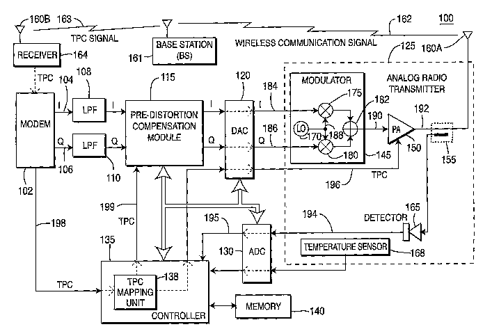
[0026] Figure 1 is a block diagram of a DBB RF transmitter 100, configured
in accordance with a preferred embodiment of the present invention. Although
the invention will be referred to in terms of being implemented upon a
transmitter 100, it should also be understood by those of skill in the art
that the
invention pertains equally to a transceiver.
[0027] Preferably, the method and system disclosed herein is incorporated
into a wireless transmitlreceive unit (WTRU). Hereafter, a WTRU includes but
is not limited to a user equipment, mobile station, fixed or mobile subscriber
unit,
pager, or any other type of device capable of operating in a wireless
environment.
-4-

CA 02528128 2005-12-05
WO 2005/002107 PCT/US2004/013906
The features of the present invention may be incorporated into an integrated
circuit (IC) or be configured in a circuit comprising a multitude of
interconnecting
components.
[0028] The present invention is applicable to communication systems using
time division duplex (TDD), time division multiple access (TDMA), frequency
division duplex (FDD), code division multiple access (CDMA), CDMA 2000, time
division synchronous CDMA (TDSCDMA), and orthogonal frequency division
multiplexing (OFDM). However, the present invention is envisaged to be
applicable to other types of communication systems as well.
[0029] As shown in Figure 1, the DBB RF transmitter 100 includes a
modem 102 which outputs an in-phase (I) signal component 104 and a
quadrature (Q) signal component 106, first and second low pass filters (LPFs)
108, 110, a digital pre-distortion compensation module 115, a least one
digital to
analog converter (DAC) 120, an analog radio transmitter 125, at least one
analog
to digital converter (ADC) 130, a controller 135 and a read-write memory 140.
[0030] The analog radio transmitter 125 includes a modulator 145, a PA
150, a coupling unit (e.g., a directional coupler or sample transmission line)
155,
an antenna 160A, a detector 165 and a temperature sensor 168. The controller
135 includes a transmit power control (TPC) mapping unit 138. The modulator
145 of the analog radio transmitter 125 includes an LO 170, first and second
modulators 1'l5, 180, and an adder 182.
[0031] In the DBB RF transmitter 100 of Figure 1, the modem 102 outputs
the I and Q signal components 104, 106, to the analog radio transmitter via
the
LPFs 108, 110, the digital pre-distortion compensation module 115, and the DAC
120. Based on the I and Q signal components 104, 106, the DAC 120 outputs an
analog real signal 184 to the first modulator 175, and an analog imaginary
signal
186 to the second modulator 180. The LO 170 of the modulator 145 provides an
LO input signal 188 to each of the first and second modulators 175, 180. The
outputs of the first and second modulators 175,180 are summed together by the
adder 182 to generate an analog complex modulated signal 190 which is input to
the PA 150. In response to receiving the analog complex modulated signal 190,
_5_

CA 02528128 2005-12-05
WO 2005/002107 PCT/US2004/013906
the PA 150 outputs an amplified communication signal 192, which is emitted
from antenna 160A of the analog radio transmitter 125 as a wireless
communication signal 162. The amplified communication signal 192 is
monitored by the detector 165 via the coupling unit 155. The detector 165
generates a feedback signal 194 which provides a detected reading having a
magnitude that is a function of the amplified communication signal 192.
[0032] The ADC 130 receives the feedback signal 194 and outputs a digital
signal 195 to the controller 135. The controller 135 controls the operation of
the
DAC 120 and the ADC 130 based on various values stored in the memory 140.
[0033] The power level of the I and Q signal components output by the
modem 102 is constant. When a BS 161 receives a wireless communication
signal 162 transmitted from the antenna 160A of the DBB RF transmitter 100,
the BS 161 compares the power of the wireless communication signal 162 to a
threshold or range established within the BS 161 in accordance with a
predetermined criteria. If the power of the wireless communication signal 162
does not meet the predetermined criteria, the BS 161 sends a wireless TPC
signal
163 to a receiver 164 having an antenna 160B which receives the wireless TPC
signal 163, and forwards a converted version (e.g., analog or digital) of the
wireless TPC signal 163 to the modem 102 of the DBB RF transmitter 100. The
receiver 164 and the DBB RF transmitter 100 may operate together (i.e., as a
transceiver) in a single WTRU, whereby antennas 160A and 160B may be
combined to form a single antenna. The TPC signal received by the modem 102
indicates how the characteristics (e.g., the power level) of the wireless
communication signal 162 should be adjusted to meet the criteria.
[0034] The modem 102 provides a TPC signal 198 to the TPC mapping unit
138 of the controller 135. The TPC signal 198 is used to compensate for
impairments incurred due to the existence of nonlinear operating
characteristics
of the PA 150. In response to receiving the TPC signal 198 (e.g., a signal
measured in decibels (dBs)), the TPC mapping unit 138 may apply a first TPC
mapped signal 199 to the digital pre-distortion compensation module 115
and/or,
via the DAC 120, apply a second TPC mapped signal 196 to the PA 150 to control
-6-

CA 02528128 2005-12-05
WO 2005/002107 PCT/US2004/013906
the amplitude of the amplified communication signal 192 by adjusting the gain
of
the PA 150. The TPC mapping unit 138 may include a plurality of LUTs,
whereby one of the LUTs is selected based on the characteristics of the TPC
signal 198 to generate the TPC mapped signals 196 and 199. For example, a
power level measured in dB which is indicated by TPC signal 198 may be
converted to a desired voltage based on information in the selected LUT of the
TPC mapping unit 138, prior to outputting the TPC mapped signal 196 at a level
corresponding to the desired voltage.
[0035] Figure 2 shows an exemplary configuration of the digital pre-
distortion compensation module 115 including a power estimation unit 205,
multipliers 210, 215, 220, 225, 230, adders 235, 240, 245, 250, a plurality of
LUTs 255 and a phase distortion compensation unit 260. The digital pre-
distortion compensation module 115 performs functions on the magnitude and
power of the I and Q signal components, whereby the input and output ports of
the digital pre-distortion compensation unit 115 have a linear (i.e., one-to-
one)
correspondence.
[0036] In the analog radio transmitter 125, the PA 150 outputs the
amplified communication signal 192 to the antenna 160A. The PA 150 has two
RF characteristics having deficiencies which are compensated for by the
digital
pre-distortion compensation module 115.
[0037] The first of the RF characteristics of the PA 150 is associated with
amplitude distortion, whereby the linearity of the PA 150 from input to output
may be deficient. If the PA 150 is perfectly linear, the amplitude
characteristics
of the amplified communication signal 192 output from the PA 150 will directly
correspond to the amplitude characteristics of the analog complex modulated
signal 190 applied to an input of the PA 150. If the amplitude of the analog
complex modulated signal 190 is continually increased, the amplified
communication signal 192 at an output of the PA 150 will eventually begin to
compress (i.e., the PA 150 reaches a saturation point), and thus the PA 150
will
no longer acts in a linear fashion which may distort one or more amplitude
characteristics of the analog radio transmitter 125, such as its dynamic
range.
_7_

CA 02528128 2005-12-05
WO 2005/002107 PCT/US2004/013906
[0038] The second of the RF characteristics is associated with phase
distortion, whereby the phase offset of the analog complex modulated signal
190
at the input of the PA 150 changes when it is amplified and output by the PA
150. This causes the amplified communication signal 192 to have an undesired
constellation rotation, whereby each point on the constellation is rotated in
the
same direction.
[0039] In a perfectly linear PA 150, the amplitude characteristics of the
output from the PA 150 will directly correspond to the amplitude
characteristics
of the analog complex modulated signal 190. In a realistic scenario, if the
amplitude of the analog complex modulated signal 190 is continually increased,
eventually the amplified communication signal 192 will begin to compress
(e.g.,
the PA 150 reaches saturation), and thus the PA 150 no longer performs in a
linear fashion.
[0040] Referring to Figure 2, the I and Q signal components are received at
power estimation unit 205 which performs a power estimate function, (e.g., I2
+
Q~). The power estimation unit 205 (I2 + Q~) outputs a power estimation signal
208 which is multiplied with the TPC mapped signal 199 via the multiplier 210,
and the resulting product signal 265 is input into a selected one of the LUTs
255
based on a temperature reading performed by the temperature sensor 168. The
selected LUT 255 has stored therein amplitude characteristics of the PA 150
associated with a particular temperature range within which the temperature
reading falls. The selected LUT 255 then outputs an amplitude compensation
signal 270 having a value Ki, based on the resulting product signal 265 and
the
known amplitude characteristics of the PA 150, as defined by the selected LUT
255. Thus, amplitude compensation is provided to eliminate deficiencies in the
analog radio transmitter 125 (i.e., due to the PA 150).
[0041] The TPC mapped signal 199 controls the output power of the analog
radio transmitter 125, as designated by the resulting product signal 265. The
amplitude compensation signal 270 is multiplied with the I and Q signal
components, respectively, via the multipliers 215 and 220, and the resulting
_g_

CA 02528128 2005-12-05
WO 2005/002107 PCT/US2004/013906
product signals 275, 280, are added to the I and Q signal components via
adders
235 and 240, respectively.
[0042] Note that the sole purpose of the adders 235, 240, is to avoid the
unintentional deactivation of the I and Q signal components should the value
of
Ki be zero.
[0043] Referring still to Figure 2, the resulting product signal 265 is also
input to the phase distortion compensation unit 260 which, in turn, outputs a
phase compensation signal 285 having a value KP to provide phase rotation.
[0044] The phase compensation signal 285 is multiplied with the I and Q
signal components, respectively, via the multipliers 225 and 230. The
resulting
product signal 290 output by the multiplier 230 is subtracted from the real
signal
component via adder 245. The resulting product signal 295 output by the
multiplier 225 is added to the imaginary signal component via adder 250.
[0045] Based on the phase compensation signal 285, the digital pre-
distortion compensation module 115 rotates the constellation such that the
real
and imaginary characteristics of the signal components are the same in all
four
quadrants of the constellation, thus forming a perfect square in the
constellation.
[0046] The digital pre-distortion compensation module 115 receives a real
(Re) I signal component and an imaginary (jIm) Q signal component and rotates
the phase of the signal components Re and jIm by KP degrees as described by
Equation 1 below:
(Re +jIm) x e'Kp Equation (1)
[0047] The outcome of the real output, R e, is described by Equation 2
below:
R a = Re - (KP x Im) Equation (2)
[0048] The output of the imaginary output, I na, is described by Equation 3
below:
I rn = Im + (Kp x Re) Equation (3)
_g_

CA 02528128 2005-12-05
WO 2005/002107 PCT/US2004/013906
[0049] Figures 3A and 3B, taken together, are a flow chart of an exemplary
process 300 which includes method steps used to adjust signals output by the
DBB RF transmitter 100. The process 300 is implemented in a wireless
communication system including a BS 161, as shown in Figure 1. The BS 161 is
configured to generate a transmit power control (TPC) signal 163 in response
to
receiving a wireless communication signal 162 from an analog radio transmitter
125 of the DBB RF transmitter 100. The BS 161 has stored therein one or more
established criteria associated with at least one expected characteristic of
the
wireless communication signal 162. When an expected characteristic such as the
power of the wireless communication signal 162 does not meet the criteria of
the
BS 161, the BS 161 generates the TPC signal 163 such that the DBB RF
transmitter will adjust the amplitude and/or phase characteristics of the
wireless
communication signal 162.
[0050] Referring to Figures 1-3B, the process 300 is implemented to adjust
the amplitude and phase characteristics of the wireless communication signal
162. In step 305, real and imaginary signal components which are used to
generate the wireless communication signal 162, are received by the power
estimation unit 205 of the pre-distortion compensation module 115. In step
310,
the power estimation unit 205 generates a power estimation signal 208 based on
the magnitude of the real and imaginary signal components (e.g., the function
I2
+ ~~ is performed). In step 315, the power estimation signal 208 is multiplied
with a first mapped TPC signal 199, via the multiplier 210, to generate a
first
resulting product signal 265. The first mapped TPC signal 199 is derived from
the TPC signal 163 generated by the BS 161.
[0051] In step 320, at least one of a plurality of LUTs 255 is selected in
response to a temperature reading performed by a temperature sensor 168
located in the analog radio transmitter 125.
[0052] In step 325, an amplitude compensation signal 270 having a value
Ki is generated by the selected LUT 255 in response to receiving the first
resulting product signal 265. In step 330, the amplitude compensation signal
270
is multiplied with the real signal component, via multiplier 215, to generate
a
-10-

CA 02528128 2005-12-05
WO 2005/002107 PCT/US2004/013906
second resulting product signal 275. In step 335, the second resulting product
signal 275 is added to the real signal component, via adder 235, to generate
an
amplitude compensated real signal component 272. In step 340, the amplitude
compensation signal 270 is multiplied with the imaginary signal component, via
multiplier 220, to generate a third resulting product signal 280. In step 345,
the
third resulting product signal 280 is added to the imaginary signal component,
via adder 240, to generate an amplitude compensated imaginary signal
component 282.
[0053] In step 350, a phase compensation signal 285 having a value Kp is
generated by the phase distortion compensation unit 260 in response to
receiving
the first resulting product signal 265. In step 355, the phase compensation
signal
285 is multiplied with the amplitude compensated real signal component 272,
via
multiplier 225, to generate a fourth resulting product signal 295. In step
360, the
fourth resulting product signal 295 is added to the amplitude compensated
imaginary signal component 282, via adder 250. In step 365, the phase
compensation signal 285 is multiplied with the amplitude compensated
imaginary signal component 282, via multiplier 230, to generate a fifth
resulting
product signal 290. In step 370, the fifth resulting product signal 290 is
subtracted from the amplitude compensated real signal component 272, via adder
245.
[0054] In step 375, a second mapped TPC signal 196 is applied to the PA
150 located within the analog radio transmitter 125 to adjust the gain of the
PA
150 such that it does not operate in a nonlinear fashion. The second mapped
TPC signal 196 is derived from the TPC signal 163 generated by the BS 161.
[0055] The process 300 runs continuously by returning to step 305 each
time the process 300 is completed. It should be understood that the process
300
is merely an example, and the order of the steps 305-375 of the process 300
may
be reconfigured as desired. For example, it may be preferred to implement step
375 prior to implementing steps 310-370.
[0056] Furthermore, it should be understood that process 300 may be
implemented on a sample-by-sample basis, whereby steps 305-375 are cycled
-11-

CA 02528128 2005-12-05
WO 2005/002107 PCT/US2004/013906
through at a sample rate substantially higher than the chip rate (e.g., ten
times
the chip rate). Values assigned to the first and second mapped TPC signals
196,
199, do not necessarily change each time the process 300 is implemented. For
example, in a TDD or other slot-based communication system, the value of the
TPC signal 198 may only be updated on a frame-by-frame basis, depending upon
the rate of updates of the value of TPC signal 163 that are provided by the BS
161. Thus, the mapping process implemented in the TPC mapping unit 138 of
the controller 135 will follow suit by updating the values of the TPC mapping
signals 196, 199, in a similar fashion.
[0057] The PA 150 outputs an amplified communication signal 192
associated with the wireless communication signal 162. The amplitude
compensation value K1 is used to correct distorted input amplitude to output
amplitude characteristics of the PA. The phase compensation value is used to
correct distorted input amplitude to output phase characteristics of the PA.
[0058] While this invention has been particularly shown and described
with reference to preferred embodiments, it will be understood by those
skilled in
the art that various changes in form and details may be made therein without
departing from the scope of the invention described hereinabove.
-12-

Dessin représentatif
Une figure unique qui représente un dessin illustrant l'invention.
États administratifs

2024-08-01 : Dans le cadre de la transition vers les Brevets de nouvelle génération (BNG), la base de données sur les brevets canadiens (BDBC) contient désormais un Historique d'événement plus détaillé, qui reproduit le Journal des événements de notre nouvelle solution interne.

Veuillez noter que les événements débutant par « Inactive : » se réfèrent à des événements qui ne sont plus utilisés dans notre nouvelle solution interne.

Pour une meilleure compréhension de l'état de la demande ou brevet qui figure sur cette page, la rubrique Mise en garde , et les descriptions de Brevet , Historique d'événement , Taxes périodiques et Historique des paiements devraient être consultées.

Historique d'événement

Description Date
Demande non rétablie avant l'échéance 2009-05-06
Le délai pour l'annulation est expiré 2009-05-06
Réputée abandonnée - omission de répondre à un avis sur les taxes pour le maintien en état 2008-05-06
Inactive : Page couverture publiée 2006-02-13
Inactive : Lettre officielle 2006-02-07
Lettre envoyée 2006-02-06
Inactive : Acc. récept. de l'entrée phase nat. - RE 2006-02-06
Lettre envoyée 2006-02-06
Demande reçue - PCT 2006-01-12
Exigences pour une requête d'examen - jugée conforme 2005-12-05
Toutes les exigences pour l'examen - jugée conforme 2005-12-05
Exigences pour l'entrée dans la phase nationale - jugée conforme 2005-12-05
Demande publiée (accessible au public) 2005-01-06

Historique d'abandonnement

Date d'abandonnement Raison Date de rétablissement
2008-05-06

Taxes périodiques

Le dernier paiement a été reçu le 2007-04-13

Avis : Si le paiement en totalité n'a pas été reçu au plus tard à la date indiquée, une taxe supplémentaire peut être imposée, soit une des taxes suivantes :

  • taxe de rétablissement ;
  • taxe pour paiement en souffrance ; ou
  • taxe additionnelle pour le renversement d'une péremption réputée.

Les taxes sur les brevets sont ajustées au 1er janvier de chaque année. Les montants ci-dessus sont les montants actuels s'ils sont reçus au plus tard le 31 décembre de l'année en cours.
Veuillez vous référer à la page web des taxes sur les brevets de l'OPIC pour voir tous les montants actuels des taxes.

Historique des taxes

Type de taxes Anniversaire Échéance Date payée
Enregistrement d'un document 2005-12-05
Requête d'examen - générale 2005-12-05
Taxe nationale de base - générale 2005-12-05
TM (demande, 2e anniv.) - générale 02 2006-05-08 2006-04-13
TM (demande, 3e anniv.) - générale 03 2007-05-07 2007-04-13
Titulaires au dossier

Les titulaires actuels et antérieures au dossier sont affichés en ordre alphabétique.

Titulaires actuels au dossier
INTERDIGITAL TECHNOLOGY CORPORATION
Titulaires antérieures au dossier
ALPASLAN DEMIR
GEETHA LAKSHMI NARAYAN
LEONID KAZAKEVICH
Les propriétaires antérieurs qui ne figurent pas dans la liste des « Propriétaires au dossier » apparaîtront dans d'autres documents au dossier.
Documents

Pour visionner les fichiers sélectionnés, entrer le code reCAPTCHA :


Pour visualiser une image, cliquer sur un lien dans la colonne description du document (Temporairement non-disponible). Pour télécharger l'image (les images), cliquer l'une ou plusieurs cases à cocher dans la première colonne et ensuite cliquer sur le bouton "Télécharger sélection en format PDF (archive Zip)" ou le bouton "Télécharger sélection (en un fichier PDF fusionné)".

Liste des documents de brevet publiés et non publiés sur la BDBC .

Si vous avez des difficultés à accéder au contenu, veuillez communiquer avec le Centre de services à la clientèle au 1-866-997-1936, ou envoyer un courriel au Centre de service à la clientèle de l'OPIC.

({010=Tous les documents, 020=Au moment du dépôt, 030=Au moment de la mise à la disponibilité du public, 040=À la délivrance, 050=Examen, 060=Correspondance reçue, 070=Divers, 080=Correspondance envoyée, 090=Paiement})


Description du
Document 
Date
(aaaa-mm-jj) 
Nombre de pages   Taille de l'image (Ko) 
Revendications 2005-12-04 17 737
Description 2005-12-04 12 661
Dessins 2005-12-04 4 119
Abrégé 2005-12-04 2 80
Dessin représentatif 2005-12-04 1 25
Accusé de réception de la requête d'examen 2006-02-05 1 177
Rappel de taxe de maintien due 2006-02-05 1 111
Avis d'entree dans la phase nationale 2006-02-05 1 202
Courtoisie - Certificat d'enregistrement (document(s) connexe(s)) 2006-02-05 1 105
Courtoisie - Lettre d'abandon (taxe de maintien en état) 2008-07-01 1 173
PCT 2005-12-04 26 1 072
Correspondance 2006-02-05 1 20
PCT 2004-05-05 1 41
Taxes 2006-04-12 1 34
Taxes 2007-04-12 1 32