Note : Les descriptions sont présentées dans la langue officielle dans laquelle elles ont été soumises.
CA 02531041 2005-12-28
WO 2005/002046 PCT/CA2004/000881
Integrated Power Amplifier Circuit
Field of the Invention
[001] The invention relates to the field of amplifier circuits, and more
specifically to
the field of integrated power amplifier circuits.
Background of the Invention
[002] Typical power amplifier (PA) technologies utilize multiple integrated
circuits
in order to provide functionality for amplification, power output control and
for
stabilization of the PA output signal level due to supply voltage and
temperature
fluctuations.
[003] It is well appreciated to those skilled in the art of amplifier design
that bias
currents supplied to the RF .signal amplification stages is are an important
determinant
of the performance of the amplification stages. For example, a bias current
supplied to
the base of a bipolar transistor acting as a RF signal amplification stage is
a major
determinant of the amplification performance demonstrated by that bipolar
transistor.
Selecting and supplying the correct bias current is crucial to optimizing the
RF signal
amplification characteristics of any transistor amplifier. Moreover, one can
appreciate
that having control over the bias current supplied to the transistor
amplifiers can enable
more sophisticated schemes for optimizing the power output characteristics of
the
transistor amplifier. For example, one might detect output power from a power
amplifier and choose to modify the bias current in response to the measured
output
power. Fuuthermore, one caal envisage other figures of merit associated with
the
performance of power amplifiers that might be optimized using control over the
bias
current, such as bias current reduction at lower output powers to improve
operating,
efficiency when RF-induced rectification currents are low.
[004] Of course, such a concept is not new to the art of power amplifier
design or
their utilization. Open-loop or close-loop control over the performance of a
power
aanplifier through the bias culTent is well known to those of slcill in the
art. Moreover,
closed loop control has been used to mitigate variations in power amplifier
output
CA 02531041 2005-12-28
WO 2005/002046 PCT/CA2004/000881
power performance in response to input control voltages, external temperature
changes,
or simply to mitigate manufacturing tolerance.
[005] Introducing a degree of control, however, over the performance of power
amplifiers through the bias current entails using additional circuitry to
convert voltage
detection error signals into incremental base voltage changes on the
transistors. That is,
circuitry is required above and beyond the transistors used for providing RF
signal
amplification. For example, introducing control over the bias current will
require, at a
minimum, circuitry for receiving the control signal and for varying the bias
current.
Numerous circuit block architectures have been discussed in the prior art for
achieving
thereof.
[006] Furthermore, all existing control architectures employ a substantial die
area,
and utilize multiple integrated circuit technologies with a net lugher
manufacturing cost
and large associated pacl~aging area. This traditional approach often results
in a
reduction in operating efficiency, due to the need for in-line coupling
circuits, and poor
repeatability of results, create more challenging calibration requirements and
reduced
manufacturing yields.
(007] If is therefore an object of the invention to provide a power amplifier
integrated circuit (PAIC) that overcomes the limitations,of the prior art by
fully
integrating such bias and power control features on a single PAIC within a
single
manufacturing process technology. The PAIC advantageously realizes a reduced
die
and pacl~aging area over existing solutions. Along with improved RF output
signal
power control repeatability versus temperature and supply voltage variations.,
Summary of the Invention
[008] In accordance with the invention there is provided a power amplifier
circuit
comprising: an input port for receiving a RF input signal; an output port for
providing
therefrom a RF output signal, the RF output signal being an amplified version
of the RF
input signal; a supply voltage input port for receiving a supply voltage; a
voltage
regulator circuit for receiving the supply voltage and for providing a
regulated supply
voltage; a first amplification stage having a first gain and for receiving one
of a signal
derived from the Rf input signal and the RF input signal and for providing a
first
CA 02531041 2005-12-28
WO 2005/002046 PCT/CA2004/000881
amplified RF signal, the first amplification stage coupled to the voltage
regulator circuit
for receiving the regulated supply voltage; and, a second amplification stage
having a
second gain and coupled to the first amplification stage for receiving one of
a signal
derived from the first amplified RF signal and the first amplified RF signal
and coupled
to the output port for providing the output signal thereto, the second
amplification stage
coupled to the supply voltage input port for receiving the supply voltage
other than
regulated by the voltage regulator circuit.
[009] fit accordance with the invention there is provided a method of
amplifying a
RF input signal to form a RF output signal that is an amplified version of the
RF input
signal comprising the steps of receiving the RF input signal; providing a
first
amplification stage having a first gain; providing a second amplification
stage having a
second gain; receiving a first supply voltage; regulating the first supply
voltage to
provide a regulated supply voltage; providing the regulated supply voltage to
the first
amplification stage; providing the first supply voltage to the second
amplification stage;
and, amplifying one of a signal derived from the received RF input signal and
the
received RF input signal using the first amplification stage having the first
gain and the
second amplification stage having the second gain to form the RF output
signal.
[0010] In accordance with the invention there is provided a power amplifier
circuit
comprising: an input port for receiving a RF input signal; an output port for
providing
therefrom a RF output signal, the RF output signal being an amplified version
of the RF
input signal; a supply voltage input port for receiving a supply voltage; a
voltage
regulator circuit for receiving the supply voltage and for providing a
regulated supply
voltage; a first amplification stage having a first gain for receiving one of
a signal
derived from the RF input signal and the RF input signal and for providing a
first
amplified RF signal, the first amplification stage coupled to the voltage
regulator circuit
for receiving the regulated supply voltage; a second amplification stage
having a
second gain for receiving one of a signal derived from the first amplified RF
signal and
the first amplified RF signal and coupled to the output port for providing the
output
signal thereto, the second amplification stage coupled to the supply voltage
input poet
for receiving the supply voltage, the supply voltage provided to the second
amplification stage and other than regulated by the voltage regulator circuit;
a
CA 02531041 2005-12-28
WO 2005/002046 PCT/CA2004/000881
temperature sensing circuit disposed for sensing a temperature of the power
amplifier
circuit and for providing a temperature signal therefrom in dependence upon
the sensed
temperature of the power amplifier circuit, the temperature signal for
provision to the
regulator circuit and at least one of the first amplification stage and the
second
amplification stage; a voltage sensing circuit disposed for sensing a
potential of the
supply voltage and for providing a sense signal in dependence thereon, the
sense signal
for provision to at least one of the regulator circuit and the first
amplification stage and
the second amplification stage; and, a control port coupled to at least one of
the voltage
regulator circuit and the first amplification stage and the second
amplification stage for
at least one of respectively controlling the regulated supply voltage and the
first gain
and the second gain.
[0011] In accordance with the invention there is provided a power amplifier
circuit
comprising: an input port for receiving a RF input signal; an output port for
providing a
RF output signal therefrom that is an amplified version of the RF input
signal; a control
port for receiving a control signal; a supply voltage input port for receiving
a supply
voltage; a temperature sensing circuit for sensing a temperature of the power
amplifier
circuit and for providing a temperature signal in dependence thereon; a
voltage sensing
circuit for sensing a potential of a voltage supply and for providing a sense
signal in
dependence thereon; a first amplification stage having a first gain for
amplifying one of
a signal derived from the RF input signal and the RF input signal to form a
first
amplified RF signal, the first amplification stage for receiving at least one
of the
temperature signal and the sense signal and the control signal and for varying
the first
gain in dependence thereon; and, a second amplification stage having a second
gain for
amplifying one of a signal derived from the first amplified RF signal and the
first
amplified RF signal to form the RF output signal, the second amplification
stage for
receiving the control signal and other than receiving at least one of the
temperature
signal and the sense signal for varying the second gain in dependence thereon.
[0012] In accordance with the invention there is provided a method of
operating a
multi amplification stage amplifier circuit comprising the steps of: receiving
of a
control signal having a control signal magnitude; providing a first
amplification stage
having a first gain; receiving one of a signal derived from a RF input signal
and a RF
CA 02531041 2005-12-28
WO 2005/002046 PCT/CA2004/000881
input signal for amplification using the first amplification stage; amplifying
the one of a
signal derived from the RF input signal and the RF input signal using the
first
amplification stage to form a first amplified RF signal, the amplifying of the
one of a
signal derived from the RF input signal and the RF input signal performed in
conjunction with a step of compensating of the first amplification stage for
at least two
of temperature and supply voltage and control signal magnitude; providing a
second
amplification stage having a second gain; receiving of the first amplified RF
signal
using the second amplification stage; and, amplifying one of a signal derived
from the
first amplified RF signal and the first amplified signal using the second
amplification
stage to form a RF output signal, the amplifying of the one of a signal
derived from the
first amplified RF signal and the first amplified signal performed in
conjunction with a
step of other than compensating of the second amplification stage for at least
one of
temperature and supply voltage fluctuations.
[0013] In accordance with the invention there is provided a power amplifier
circuit
comprising: an input port for receiving a RF input signal; an output port for
providing a
RF output signal therefrom that is an amplified version of the RF input
signal; a control
port for receiving a control signal; a supply voltage input port for receiving
a supply
voltage; a temperature sensing circuit for sensing a temperature of the power
amplifier
circuit and for providing a temperature signal in dependence thereon; a
voltage sensing
circuit for sensing a potential of a voltage supply and for providing a sense
signal in
dependence thereon; a first amplification stage having a first gain and for
amplifying
one of a signal derived from the RF input signal and the. RF input signal to
form a first
amplified signal, the first amplification stage for receiving at least one of
the
temperature signal and the sense signal and the control signal and for varying
the first
gain in dependence thereon; and, a second amplification stage having a second
gain and
for amplifying one of a signal derived from the first amplified signal the
first amplified
signal, the second amplification stage for receiving at least one of the
control signal and
the temperature signal and the sense signal for varying the second gain in
dependence
thereon, the second amplification stage coupled directly to the supply voltage
input
port.
CA 02531041 2005-12-28
WO 2005/002046 PCT/CA2004/000881
[0014] In accordance with the invention there is provided a method of
operating a
poly stage amplifier circuit comprising the steps of: providing of a first
amplification
stage having a first gain and for receiving one of a signal derived from a RF
input
signal and a RF input signal for amplification; amplifying the one of a signal
derived
from the RF input signal and the RF input signal using the first amplification
stage to
form a first amplified signal, the amplifying of the one of a signal derived
from the RF
input signal and the RF input signal performed in conjunction with a step of
compensating of the first amplification stage for at least one of temperature
and supply
voltage fluctuation and control signal magnitude; providing of a second
amplification
stage having a second gain and for receiving one of a signal derived from the
first
amplified signal and the first amplified signal; supplying the supply voltage
to the
second amplification stage without a substantial voltage drop between a
potential of the
supply voltage and that received by the second amplifying stage; and,
amplifying the
signal derived from the first amplified signal and the first amplified signal
using the
second amplification stage to form a RF output signal, the amplifying of the
signal
derived from the first amplified signal and the first amplified signal
performed in
conjunction with a step of compensating of the second amplification stage for
at least
one of temperature and supply voltage fluctuations.
[0015] In accordance with the invention there is provided aaz amplifier
circuit for
receiving an input signal for amplification comprising: an input port for
receiving a RF
input signal; an output port for providing a RF output signal therefrom that
is an
amplified version of the RF input signal; a control poet for receiving a
control signal; a
supply voltage input port for receiving a supply voltage; a regulator circuit
for
receiving the supply voltage and for providing a regulated supply voltage in
dependence upon at least one of a temperature of the amplifier circuit, the
supply
voltage, and the regulated supply voltage, where at least one of the
temperature signal,
the supply voltage and the regulated supply voltage are provided to the
regulator circuit
using a direct feedbaclc path; at least a first amplification stage and a
second
amplification stage, the at least a first amplification stage and the second
amplification
stage coupled to at least one of the supply voltage and the regulated supply
voltage, the
first amplification stage for receiving one of a signal derived from the RF
input signal
and the RF input signal and for providing a first amplified signal, to the
second
CA 02531041 2005-12-28
WO 2005/002046 PCT/CA2004/000881
amplification stage, the second amplification stage for amplifying a signal
derived from
the first amplified signal and the first amplified signal to form the RF
output signal.
[0016] In accordance with the invention there is provided a method of
operating a
multi stage amplifier circuit comprising the steps of: receiving a RF input
signal;
receiving a supply voltage; receiving a control signal; receiving at least one
of a
temperature signal related to a temperature of the amplifier circuit and a
sense signal
related.to the supply voltage; regulating the received supply voltage to form
a regulated
supply voltage in dependence upon the received at least one of temperature
signal and
sense signal; providing a first amplification stage having a first gain;
providing a
second amplification stage having a second gain; providing the regulated
supply
voltage to at lease one of the first amplification stage and the second
amplification
stage; and, amplifying one of a signal derived from the received RF input
signal and the
received RF input signal using the first amplification stage and the second
amplification
stage to form a RF output signal that is an amplified version of the one of a
signal
derived from the received RF input signal and the RF input signal.
Brief Description of the Drawings
[0017] Exemplary embodiments of the invention will now be described in
conjunction with the following drawings, in which:
[0018] FIG. 1 illustrates a prior art utilizing a power amplifier circuit, an
external
feedback circuit and an external output power detection circuit;
[0019] FIG. 2 illustrates a prior art PA circuit utilizing a voltage
regulation circuit for
controlling an output power of a RF output signal emitted from the PA;
[0020] FIG. 3 illustrates a PA circuit that utilizes an external current
sensing circuit;
[0021] FIG. 4 illustrates a first embodiment of the invention, a Dual Feedback-
Low
power regulation circuit for a three stage PAIL;
[0022] FIG. 5 illustrates a second embodiment of the invention, a three stage
RF PA
formed in a PAIL with a current source feedback circuit having low RF output
signal
power regulation; and,
CA 02531041 2005-12-28
WO 2005/002046 PCT/CA2004/000881
[0023] FIG. 6 illustrates a third embodiment of the invention, a three stage
RF PA
formed in a PAIC die in conjunction with an integrated logaritlnnic detector
circuit,
integrated into the same die.
Detailed Description the Invention
[0024] FIG. 1 illustrates a prior art power amplifier (PA) integrated circuit
(IC)
(PAIL) 101, a compaxator circuit 102, and a RF power detection circuit 103.
The PAIC
101 has an input port lOla for receiving a RF input signal, an output port
101b for
providing a RF output signal therefrom, a supply voltage input port lOld for
receiving
a supply voltage and a control port 101 c for receiving a control signal.
Disposed within
the PAIC '101 are a first amplification stage 121, a second amplification
stage 122, and
a tlurd amplification stage 123. Each amplification stage comprises a
transistor having
a base terminal coupled to one of an input port and a collector terminal of a
previous
amplification stage using a capacitor. Capacitor 131 is used to couple the RF
input
signal to the first amplification stage, and capacitors 132, 133 are used to
couple the
amplification stages together. Additionally, the first amplification stage 121
has
disposed therein a first current source 111, the second amplification stage
122 has
disposed therein a second current source 112, and the third amplification
stage has
disposed therein a third current source 113. The first, second and third
current sources
are for providing first, second and third bias currents to first, second and
third
amplification stages. More specifically in this embodiment of a bipolax
transistor based
amplifier circuit, the first, second and third currents are provided to the
base terminals
of the first, second and third transistors disposed within the three
amplification stages,
respectively. An integrated temperature sensing circuit (ITSC) 104 is
integrated within
the PAIC 101 for sensing a temperature of the die having the PAIC 101 disposed
therein and for providing a first temperature signal therefrom, in response to
a
temperature of the die on which the power amplifier circuit is formed. The
first
temperature signal is provided to the first current source 111, second current
source 112
and third current source 113.
[0025] The control input port l Olc is coupled to each of the current sources,
such that
the current sources each receive the control signal therefrom. Each current
source is for
CA 02531041 2005-12-28
WO 2005/002046 PCT/CA2004/000881
varying its current provided to its corresponding amplification stage in
dependence
upon the control signal and the first temperature signal.
[0026] Each amplification stage is disposed between the supply voltage input
port
l Old and a ground potential. A transistor is disposed in each amplification
stage with
its collector terminal coupled to the supply voltage input port 101 d and the
emitter
terminal thereof coupled to ground. The transistor disposed within the third
amplification stage 123 has its collector terminal coupled to the output port
l Olb and its
base terminal capacitvely coupled to the collector terminal of the transistor
disposed
within the second amplification stage. The transistor disposed in the first
amplification
stage has its base temninal capacitvely coupled to the input port 101 a using
capacitor
131. The output port lOlb is additionally coupled to the supply voltage input
port lOld.
[0027] It is often the case that the PAIC 101 is formed on a GaAs substrate,
while the
RF power detection circuit 103 having a detector diode 105 disposed therein
for
receiving a portion of the RF output signal current emitted from the PAIL
output port
lOlb, is formed on a silicon substrate. The comparator circuit 102 is formed
on a
silicon substrate, or on an FR4 glass-fiber type substrate, and is for
receiving a diode
output voltage proportional to RF output signal power. Unfortunately, at least
three
different substrates are utilized for implementing of the PAIC 101, the RF
power
detection circuit, and the feedbaclc circuit 102. Moreover, the bias current
sources, and
temperature sensing circuits, are often disposed upon another substrate. Thus,
bondwires between the substrates are required in the fnushed device, which
increases
associated manufacturing costs.
[0028] In operation, for stabilizing of the RF output signal power of the PAIC
101,
the diode output voltage is compared to a target signal and the comparator
circuit 102
provides the control to the control port 101 c of the PAIL 101 in response
thereto. In
dependence upon the control signal, the first, second and third bias currents,
and the
first temperature signal, the PAIL 101 amplifies the RF input signal based
upon a gain
of each amplification stage to provide the RF output signal.
[0029] Additionally, traditional control characteristics for controlling of
the GaAs PA
result in large changes in output signal power in dependence upon small
changes in
CA 02531041 2005-12-28
WO 2005/002046 PCT/CA2004/000881
control signal voltage. This poses a design challenge in designing a control
loop that
offers PA stability for various operating temperatures of the PA die. In
addition, a
tangential response of the diode detector causes the rate of change of diode
output
signal voltage to be reduced at low RF output signal power levels, which
results in
timing mask challenges in certain transmit architectures, such as GSM.
[0030] A second prior art architecture, as illustrated in FIG. 2, implements
an off
chip voltage regulator circuit 202 for controlling an output power of a RF
output signal.
A power amplifier integrated circuit 201 is provided with an input port 201 a
for
receiving a RF input signal, an output port 201b for providing a RF output
signal
therefrom, and a regulated voltage input port 201 c for receiving a regulate
positive
supply voltage from the off chip voltage regulator circuit 202.
[0031] The regulator circuit 202 has a supply voltage input port 202b for
receiving a
supply voltage from a power supply (not shown) coupled thereto. A control port
202a is
disposed on the regulator circuit 202 for receiving a control signal. Within
the regulator
circuit 202 there is disposed an operational amplifier (OpAmp) 203 having a
first input
port coupled with the control pout 202a for receiving the control signal and
an output
port of the OpAmp 203 is coupled to a gate terminal of a FET 204. Optionally a
difference amplifier is disposed in a similar manner to the OpAmp 203 and
replaces the
OpAmp 203. Drain and source terminals of the FET 204 are disposed in series
between
the positive supply voltage input port 202b and a regulated supply voltage
output port
202c. A feedback sense circuit 205 is disposed between a second input port of
the
OpAmp 203 and the regulated supply voltage output port 202c. The regulated
supply
voltage output port 202c is coupled to the regulated supply voltage input port
201c for
receiving the regulated supply voltage from the regulator circuit 202.
[0032] Disposed within a same PAIL die 201 are a first amplification stage
221, a
second amplification stage 222 and third amplification stage 223. In this
embodiment
of a power amplifier using bipolar transistors, each amplification stage
comprises a
transistor having a base terminal coupled to one of am input port and a
collector
terminal of a previous amplification stage. The amplification stages are
capacitively
coupled using capacitors 231, 232, 233. Capacitor 231 is used to couple the RF
input
signal to the first amplification stage 221. Additionally, the first
amplification stage 221
to
CA 02531041 2005-12-28
WO 2005/002046 PCT/CA2004/000881
has disposed therein a first current source 21 l, the second amplification
stage 222 has
disposed therein a second current source 212, and the third amplification
stage has
disposed therein a third current source 213. An integrated temperature sensing
circuit
(ITSC) 204 is integrated within the PAIC die 201 for sensing a temperature. of
the die
of the PAIC 201 and for providing a first temperature signal in response to
the
temperature of the die. The first temperature signal is provided to the first
current
source 211, the second current source 212 and tlurd current source 213.
(0033] Each current source is for varying its bias current provided to each
amplification stage in dependence upon the received first temperature signal.
Each
amplification stage is disposed between the regulated supply voltage input
port 201c,
for receiving the regulated supply voltage from the regulator circuit 202, and
a ground
potential. Each transistor within each amplification stage has its collector
terminal
coupled to the regulated supply voltage input port 241 c and the emitter
terminal thereof
coupled to ground. The transistor forming the third amplification stage 223
has its
collector terminal coupled to the PAIC output port 201b. The base terminal of
the '
transistor disposed within the first amplification stage 221 has its base
terminal
capacitvely coupled to the PAIC input port 201 a using capacitor 231. The PAIL
output
port 201b is additionally coupled to the to the reduced positive supply
voltage input
port 201 c.
[0034] The regulator IC 202 employs a low drop out (LDO) regulator circuit in
series
with a collector terminal of the transistors disposed witlun the amplification
stages of
the PAIC 201. The FET 204 disposed within the regulator circuit is typically
in the
form of a silicon PMOS transistor, which in conjunction with the OpAmp 203,
provides
specific bandwidth compensated regulated supply voltage to the amplification
stages of
the PAIC 201. The amplification stages of the PAIC are typically formed on a
separate
GaAs substrate from the regulator circuit 202. Due to the high saturation
current and
low ON resistance requirements of the regulator IC 202 for providing a low
resistance
signal path to the collector terminals of the transistors forming each of the
amplification
stages, a large area PMOS die is utilized for implementing of the regulator IC
202,
resulting in a high manufacturing cost and a high overall module size.
Unfortunately,
with the size of the regulator circuit IC 202 and regulator IC circuit
technology
11
CA 02531041 2005-12-28
WO 2005/002046 PCT/CA2004/000881
requirements, along with the poor thermal isolation characteristics of the
amplification
stages, the regulator IC 202 is prevented from being integrated on the same
die as the
PAIC 202.
[0035] A third prior art arclutecture, which utilizes an off chip cuiTent
sense IC 302
for sensing current consumed by circuit elements forming the PAIC 301, is
illustrated
in FIG. 3. The sense IC 302 is on a separate die than the PAIC 301. An input
poet 301a
is formed on the PAIL 301 for receiving a RF input signal, an output port 301b
is
provided for providing an amplified version of the input signal in the form of
an
amplified RF output signal therefrom, and a voltage input port 301d is
disposed on the
PAIC for receiving a supply voltage from a power supply (not shown) connected
thereto.
[0036] The current sense IC 302 is provided with a supply voltage input port
302a for
receiving a voltage from a power supply (not shown) coupled thereto. A sense
resistor
304 is disposed between the voltage input port 302a and a reduced voltage
output port
302c. The reduced voltage output port 302c is coupled to the output port 301b
of the
PAIC for providing a reduced supply voltage to the third amplification stage.
A
differential sensing amplifier 303 is disposed within the sense IC 302 and has
its input
ports disposed in parallel with the sense resistor 304 for measuring a voltage
drop
thereof. An output port of the differential sensing amplifier 303 is coupled
to a sense
signal output port 302b for providing a sense signal therefrom. As a third
amplification
stage 323 draws more current, the voltage drop across the sense resistor
increases.
[0037] A sense signal input port 301e is also provided for coupling off chip
to the
sense signal output port 302b. Disposed within the PAIC 301 are a first
amplification
stage 321, a second amplification stage 322 and the third amplification stage
323. In
this embodiment of a power amplifier using bipolar transistors each
amplification stage
comprises a transistor having a base terminal capacitively coupled to one of
an input
port and a collector terminal of a previous amplification stage. Capacitors
331, 332, 333
are provided for facilitating capacitive coupling of the amplification stages.
Capacitor
331 is disposed for coupling the RF input signal to the first amplification
stage.
Additionally, each amplification stage has disposed therein a first current
source 31 l, a
second cutTent source 312 and a third current source 313, for providing first,
second
12
CA 02531041 2005-12-28
WO 2005/002046 PCT/CA2004/000881
and third bias currents. The first, second and third bias currents are
provided to the base
terminals of first, second and third transistors disposed within the three
amplification
stages. An integrated temperature sensing circuit (ITSC) 304 is integrated
within a die
of the PAIC 301 for sensing a temperature of the die and for providing a first
temperature signal in response to the temperature of the die. The first
temperature
signal is provided to the first current source 31 l, second current source 312
and third
current source 313. The control port 301 c is coupled to each of the cttiTent
sources for
receiving the control signal.
[0038] Each current source is for varying the current provided to a respective
amplification stage in dependence upon the received temperature signal, the
control
signal received from a control port 301c, and a sense signal received from the
off chip
sense IC 302 via the sense signal input port 301e. The first amplification
stage 321 and
the second amplification stage 322 are disposed between the positive supply
voltage
input port 301 d, for receiving a positive supply voltage from the power
supply (not
shown) coupled thereto, and ground. A second transistor disposed within the
second
amplification stage 322 has its collector terminal capacitively coupled, using
capacitor
333, to the base terminal of the tlurd transistor disposed within the third
amplification
stage 323. A collector terminal of a third transistor disposed within the
third
amplification stage 323 is coupled to the output port 301b and to the reduced
voltage
output port 302c.
[0039] This prior art circuit illustrated in FIG. 3, which utilizes the
current sensing
approach via the sense resistor 304, also has substantial performance
limitations. A first
limitation lies in that a voltage drop realized across the sense resistor 304
disposed in
the sense IC 302 results in the sensing IC 302 having a loss in operating
efficiency for
the PAIC 301 for all RF output signal power levels. In order to minimize this
inefficiency, the sense resistor 304 has a low resistance value such that a
substantial
voltage drop is not realized between the DC potential provided to the
collector
terminals of the transistors and the DC potential provided to the PAIC output
port 301b.
However, as a result of the resistance value of the sense resistor 304, both
tolerance and
dynamic range issues associated therewith axe relevant to PAIL performance.
Furthermore, because of the low resistance value of the sense resistor 304,
the
13
CA 02531041 2005-12-28
WO 2005/002046 PCT/CA2004/000881
manufacturing tolerance results in differences in detected output signal power
levels for
a given control voltage from one manufactured sense IC unit to another. The
small
resistance value additionally affects output signal power accuracy at low
output signal
power levels due to the extremely small voltage drop realized across the sense
resistor
304 and the ability of the differential sensing amplifier 303 to measure this
voltage drop
accurately. As a result of the manufacturing tolerances from sense IC unit to
sense IC
unit, for a same control signal, a different magnitude sense signal results
due to the
manufacturing difference in the sense resistances.
[0040] FIG. 4 illustrates a Dual Feedback-Low power regulation circuit for a
three-
stage power amplifier integrated circuit (PAIC) 401 in accordance with a first
embodiment of the invention. The PAIL 401 preferably has integrated therein a
regulator circuit 405, in the form of a reduced die area regulator circuit,
which is
formed within the same die as the PAIL 401. The PAIC 401 is provided with an
input
port 401a for receiving a RF input signal, an output poet 401b for providing a
RF output
signal, in the form of an amplified version of the RF input signal therefrom,
a supply
voltage input port 401 d for receiving a supply voltage, and a control port
401 c for
receiving a control signal from an external source (not shown).
[0041] A voltage sensing circuit 406 is preferably disposed in series between
the
voltage input port 401 d and the integrated regulator circuit 405, where the
integrated
regulator circuit is preferably in the form of an integrated compact low
dropout (LDO)
voltage regulator circuit. Preferably, the voltage sensing circuit 406 is
integrated on the
same die as the PAIC 401. The. integrated regulator circuit 405 receives the
supply
voltage from the voltage input port 401d and provides a regulated supply
voltage
therefrom. The voltage sensing circuit 406 provides a voltage sense signal in
dependence upon a sensed potential of the supply voltage.
[0042] Preferably, within the integrated regulator circuit 405, there is
disposed an
operational amplifier (OpAmp) 403 having a first input port coupled with the
control
port 401c for receiving the control signal. Optionally, the OpAlnp is replaced
with a
difference amplifier. An output port of the OpAmp 403 is coupled to a gate
terminal of
a FET 404. The FET 404 drain and source terminals are disposed in series
between the
voltage sensing circuit 406 and the junction 404a formed at the collector
terminals of a
14
CA 02531041 2005-12-28
WO 2005/002046 PCT/CA2004/000881
first transistor disposed within a first amplification stage 421 and a second
transistor
disposed within a second amplification stage 422. A second input port of the
OpAmp
403 is coupled to an output port of a first summing circuit 407. A first input
port of the
first summing circuit 407 is for coupling to the junction 404a formed between
one of
the drain and source terminals of the FET 404 and the collector terminals of
the first
and second transistors disposed within the first and second amplification
stages, 421
and 422, respectively. A second input port of the first summing circuit 407 is
for
receiving the voltage sense signal from the voltage sensing circuit 406.
Junction 404a
receives the regulated supply voltage from the integrated regulator circuit
404.
[0043] In addition to the first amplification stage 421 and the second
amplification
stage 422, a third amplification stage 423 is disposed within the PAIC 401 and
integrated therewith on the same die. In this embodiment of a power amplifier
circuit
using bipolax transistors, each amplification stage comprises a transistor
having a base
terminal coupled to one of an input port and a collector terminal of a
previous
amplification stage, using capacitive coupling. Capacitors 431, 432, 433 are
provided
for facilitating the capacitive coupling. Capacitor 431 is disposed between
the input
port 401 a and the first amplification stage 421 for capacitively coupling of
the RF input
signal into the PAIL 401, and second and third capacitors 432 and 433 act to
capacitively couple the second and tlurd amplification stages together.
Additionally, the
three amplification stages have disposed therein a first current source 411, a
second
current source 412 and third current source 413, for providing first, second
and third
bias currents to the base terminals of first, second amd third transistors,
respectively.
The three amplification stages are thus provided with first, second and third
gains,
respectively, in response to the first, second and third bias currents.
(0044] An integrated temperature sensing circuit (ITSC) 40~ is integrated
within the
same die as the PAIC 401 and is for sensing a temperature of the die and for
providing
an at least a temperature signal in response to a temperature thereof. The at
least a
temperature signal is in the fomn of a first temperature signal and a second
temperature
signal, where the first temperature signal is provided to the first current
source 411 and
to the second current source, and where the second temperature signal is
provided to a
third input port of the first summing circuit 407. The PAIL output port 401b
is
CA 02531041 2005-12-28
WO 2005/002046 PCT/CA2004/000881
additionally coupled to the positive voltage input port 401d for receiving a
DC bias
voltage for biasing of the third transistor collector terminal.
[0045] The first, second and tlurd cuzTent sources are additionally coupled to
the
control port 401 c for receiving the control signal. The first current source
411 and the
second current source 412 axe for varying their bias current provided to the
first and
second amplification stages in dependence upon the received first.temperature
signal,
the voltage sense signal, and the control signal. The third cuiTent source 413
is coupled
to the control port 401 c for preferably having its magnitude vaxied only in
response to
the control signal.
[0046] To compensate for output signal power due to changes in temperature of
the
PAIL die, an indirect feedback loop is employed, which compensates the first
and
second amplification stages for temperature in order to maintain a fixed RF
output
signal power at the output port 401b. In use, as heating of the die occurs due
to the third
gain of the third amplification stage, the temperature of the PAIC die
increases in
response to the power dissipated by the third amplification stage. This change
in
temperature is reflected in the first and second temperature signals generated
by the
ITSC 408. Thus, the first and second amplification stages provide a
precompensated
signal to an input port of the third amplification stage in order to
precompensate the
input signal to the third amplification stage for both power supply variations
and PAIC
die temperature variations. Furthermore, if the PAIL die is subject to heating
from an
external source, then the precompensated signal provided to the third
amplification
stage is reflective of this heating.
[0047] In use, a control signal in the form of a ramp voltage is applied to
the control
port 401 c. The control signal is for achieving a desired target RF output
signal power
by controlling the first, second and third gains of the amplification stages
within the
PAIL 401. The ramp voltage provides wzde dynamic range performance for the
PAIC
401 by varying the gain of the multi-stage PAIL through two means. The primary
means of gain control is through variation of the regulated supply voltage
provided to
junction 404a, based on the control signal received from the control port
401c~. The
secondary means of gain variation is achieved tlirough modification of the
bias currents
provided from each of the three current sources 411, 412, and 413, where the
three bias
16
CA 02531041 2005-12-28
WO 2005/002046 PCT/CA2004/000881
currents are proportional to a parameter of the control signal received at the
control port
401 c. Regulator circuit 405 control of the first amplification stage 421 and
second
amplification stage 422 provides precise RF signal power control proportional
to the
square of the voltage on the collector terminals of the first and second
transistors. This
precisely controlled RF signal power is incident on the third amplification
stage 423
and further amplified using the third amplification stage, in a controlled
manner,
through the action of third current source 413 and third transistor 423. The
presence of
the regulator circuit 405 results in RF signal power emitted from the first
and second
amplification stages to be precisely known and independent of supply voltage
variations occurring at the supply voltage input port 401 d. However, in order
to
compensate for the effects of supply voltage variation occurring at the third
amplification stage, the sense circuit 406 is employed, which provides the
sense signal
to the first sunnning circuit 407 disposed in the regulator circuit 405. The
input signal
provided to the third amplification stage reduces the low dropout (LDO), which
maintains the gain of the third stage constant. Sensing the temperature of the
PAIC die
provides a further compensation factor for the regulator circuit 405. Sensing
the
temperature removes temperature variation from the RF signal power incident at
the '
third amplification stage 423. Additionally, by optionally providing the
temperature
signal to the first and second current sources, fme-tuning of the temperature
and voltage
effects of the PAIL 401 axe achieved.
[0048] Thus, RF input signal power provided to the third amplification stage
is
continuously compensated in order to maintain a desired RF output signal power
by
varying the first and second bias currents as well as the collector terminal
voltages
using the regulator circuit 405. The third stage transistor base current is
slowly varied
proportional to the control signal ramp voltage in order to minimize consumed
current
at low signal powers and to adequately drive the base terminal at high powers,
thus
achieving the desired dynamic range. This advantageously results in a
substantial
reduction in die area and module size, by removing the need for regulation of
the final
power stage as well as simplified calibration requirements for calibrating of
the control
signal in relation to RF output signal power. Further advantageously, a
reduced thermal
load is realized and improved PA amplification efficiency is achieved for
reduced
output signal power levels. The substantial reduction in the die axea results
from a
1~
CA 02531041 2005-12-28
WO 2005/002046 PCT/CA2004/000881
smaller area FET 404 that is utilized within the regulator circuit 405. The
FET 404 is of
a smaller size because only the first and second amplification stages are
regulated using
the regulated supply voltage and not the lugher-powered third amplification
stage. In
regulating the supply voltage to the third amplification stage, much larger
area FET
devices are used in order to handle the higher power requirements of this
third
amplification stage. As is known to those of skill in the art, the third, or
final
amplification stage, typically has a regulated supply voltage provided
thereto.
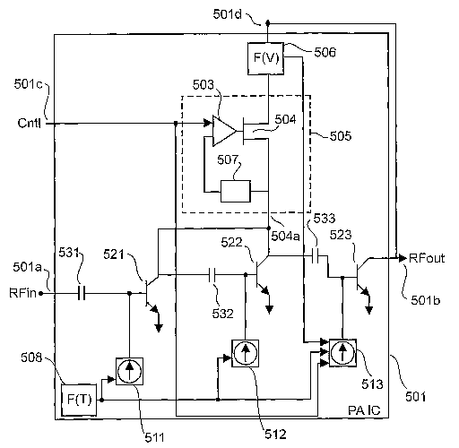
[0049] FIG. 5 illustrates a current source feedback circuit having low RF
output
signal power regulation for a three stage power amplifier integrated circuit
(PAIL) 501
in accordance with a second embodiment of the invention. The PAIC 501
preferably
has integrated therein a regulator circuit 505, in the form of a reduced die
area regulator
circuit, which is formed within a same substrate as the PAIC 501. The PAIC 501
is
provided with a PAIC input port SOla for receiving a RF input signal, a PAIC
output
port SOlb for providing an amplified RF output signal therefrom, a voltage
input port
S o l d for receiving a supply voltage, and a control pout S O l c for
receiving a control
signal from an external source (not shown).
[0050] A voltage sense circuit 506 is preferably integrated on the same die
with the
PAIL 501 and disposed in series between the supply voltage input port SOld and
the
integrated regulator circuit 505. The integrated regulator circuit 505
receives the supply
voltage through the supply voltage input port SOld and provides a regulated
supply
voltage therefrom. The voltage sensing circuit'S06 provides a sense signal
therefrom.
[0051] Within the integrated regulator circuit 505 there is disposed an
operational
amplifier (OpAmp) 503 having a first input port coupled with the control port
SOlc for
receiving the control signal. Optionally, the OpAmp is replaced with a
difference
amplifier. An output port of the OpAmp 503 is coupled to a gate terminal of a
FET 504.
The FET drain and source terminals are disposed in series between the voltage
sense
circuit 506 and a junction 504a formed between a collector terminal of a first
transistor
disposed within a first amplification stage 521 and a second transistor is
disposed
within a second amplification stage 522. A second input port of the OpAmp 503
is
coupled to an output port of a feedback sense circuit 507. An input port of
the feedback
sense circuit 507 is coupled to the junction formed between the collector
terminals of
18
CA 02531041 2005-12-28
WO 2005/002046 PCT/CA2004/000881
the first and second transistors disposed within a first amplification stage
and a second
amplification stage, respectively, and one of the gate and drain terminals of
the FET
504.
[0052] hi addition to the first amplification stage 521 and the second
amplification
stage 522, a third amplification stage 523 is disposed within the PAIC 501 and
integrated therewith on the same die. Each amplification stage comprises a
transistor
having a base terminal coupled to one of an input port and a collector
terminal of a
previous amplification stage using a capacitive coupling. Capacitors 531, 532,
533 are
provided for facilitating the capacitive coupling. Capacitor 531 is disposed
between the
input port 501 a and the first amplification stage 521 for capacitively
coupling of the RF
input signal to the first amplification stage. Additionally, the amplification
stages have
respectively disposed therein a first current source 511, a second current
source 512 and
a third cut~rent source 513, for providing first, second and third bias
currents to the base
terminals of first, second and third transistors, respectively. The three
amplification
stages are thus provided with first, second and third gains, respectively, in
response to
the first, second and third bias currents.
[0053] An integrated temperature sensing circuit (ITSC) 508 is integrated
within the
die of the PAIC 501 for sensing a temperature of the die and for providing at
least a
temperature signal therefiom in response to a temperature of the die. The at
least a
temperature signal is in the form of a first temperature signal, where the
first
temperature signal is provided to the first current source 511, the second
current source
512, and the third current source.513. The third current source 513 is
additionally
coupled to the control port SOlc for receiving the control signal and to the
voltage sense
circuit 506 for receiving the voltage sense signal. The output port SOlb is
additionally
coupled with the supply voltage input port SOld for receiving a DC bias
voltage
therefrom for the collector terminal of the third transistor disposed within
the third
amplification stage 523.
[0054] The first and second current sources are for varying their first and
second bias
current provided to the first and second amplification stages in dependence
upon the
received first temperature signal. The third current source is for varying its
third bias
19
CA 02531041 2005-12-28
WO 2005/002046 PCT/CA2004/000881
current in dependence upon the first temperature signal, the control signal
and the
voltage sense signal.
[0055] To compensate for RF output signal power variation due to changes in
temperature of the PAIL die, a direct feedback path is employed for providing
the
temperature signal to all three current sources. To compensate for RF output
signal
power variation due to changes supply voltage, the first and second
amplification stages
receive the regulated supply voltage. Thus, the first and second amplification
stages
provide a partially precompensated signal to the third amplification stage. In
use, as
heating of the die occurs due to the third gain of the third amplification
stage, the
temperature of the PAIC die increases in response to the power dissipated by
the third
amplification stage. This change in temperature is reflected in the
temperature signal
generated by the ITSC 508.
[0056] This embodiment also employs a similar technique for compensating of
the
RF output signal propagating from the third stage as disclosed in the first
embodiment,
but additionally utilizes a feedbaclc signal, in the form of the voltage sense
signal. As
implemented in the first embodiment, a ramp voltage is applied to the control
port SOlc
for controlling a magnitude of the third current provided from the third
current source
513 to the third amplification stage 523. The voltage sense signal is
additionally
provided to the third current source for compensating the RF output signal
emitted from
the third amplification stage for supply voltage variations.
[0057] In use, a control signal in the form of a ramp voltage is applied to
the control
port 501c. The control signal is used for achieving a desired target RF output
signal
power by controlling the first, second and third gains of the amplification
stages within
the PAIC 501. The ramp voltage provides wide dynamic range performance for the
PAIC 501 by varying the gain of the multi-stage PAIC through two means. The
primary means of gain control is through variation of the regulated supply
voltage
provided to junction 504a, based on the control Signal received from the
control port
SOlc. The secondary means of gain control is achieved through modification of
the bias
currents provided from each of the three current sources 511, 512, and 513,
where the
three bias currents are proportional to a parameter of the control signal.
Regulator
circuit 505 control of the first amplification stage 521 and second
amplification stage
CA 02531041 2005-12-28
WO 2005/002046 PCT/CA2004/000881
522 provides precise output power control proportional to the square of the
voltage on
the collector terminals of the first and second transistors. This precisely
controlled RF
signal power is incident on the third amplification stage 523 and further
amplified using
the third amplification stage in a controlled manner through the action of
third current
source 513 and third transistor 523. The presence of the regulator circuit 505
results in
output signal power emitted from the first and second amplification stages to
be
precisely l~nown and independent of supply voltage variations occurring at the
supply
voltage input port SOld. However, in order to compensate for the effects of
supply
voltage variation occurring at the third amplification stage, the sense
circuit 506 is
employed, which provides the sense signal to the third current source 513 for
fine
tuning of the third gain. The input signal provided to the third current
source reduces
.the required size of the regulator circuit 505 in the form of a low dropout
(LDO) circuit,
and maintains the gain of the third stage constant. Sensing the temperature of
the PAIC
die provides a final compensation factor for three current sources. Sensing
the
temperature removes temperature variation from the RF signal power emitted
from the
output port SOlb.
[005] This circuit implementation of the second embodiment advantageously
results
in a substantial reduction in die and module size. The substantial reduction
in the die
area results from a smaller area FET that is utilized within the regulator
circuit. The
FET is of a smaller size because only the first and second amplification
stages axe
regulated using the regulated supply voltage and not the higher-powered third
amplification stage. Because of reduced current requirements of the first and
second
amplification stages, the regulator circuit occupies a small die area. It is
known to those
of skill in the art that in regulating the supply voltage to the third
amplification stage, a
much larger die area FET is used in order to handle the higher power
requirements of
the third amplification stage. Furthermore, the second embodiment offers
simplified
calibration requirements, reduced thermal load, and improved amplification
efficiency
at reduced RF output signal power levels.
[0059] FIG. 6 illustrates a detector circuit, in the form of an integrated
logarithmic
detector circuit 610, disposed in conjunction with a three stage power
amplifier
integrated circuit (PAIC) 601 in accordance with a third embodiment of the
invention.
21
CA 02531041 2005-12-28
WO 2005/002046 PCT/CA2004/000881
The third embodiment of the invention has an integrated regulator circuit 605,
in the
form of a reduced die area regulator circuit, which is formed in a same
substrate as the
PAIC 601. The PAIC 601 is provided with an input port 601 a for receiving. a
RF input
signal, a PAIC output port 601b is for providing an amplified version of the
RF input
signal in the form of a RF output signal. A supply voltage input port 601 d is
provided
for receiving a supply voltage, and a control port 601c is disposed therein
for receiving
a control signal from an external source (not shown).
[0060] The integrated regulator circuit 605 is preferably integrated with the
PAIC
601 and coupled to the supply voltage input port 601 d for receiving a supply
voltage
therefrom from a power supply (not shown) coupled thereto. The integrated
regulator
circuit 605 provides a regulated supply voltage therefrom to a junction 604a.
Within the
integrated regulator circuit 605 there is disposed an operational amplifier
(OpAmp) 603
having a first input port coupled with the control port 601c for receiving the
control
signal. An output port of the OpAmp 603 is coupled to a gate terminal of a FET
604.
The FET drain and source terminals are disposed in series between the supply
voltage
input port 601d and collector terminals of a junction 604a formed between
collector
terminals of a first transistor disposed within a first amplification stage
621 and a
second transistor disposed within a second amplification stage 622. A second
input poet
of the OpAmp 603 is coupled to an output port of a feedback sense circuit 607.
An
input port of the feedback sense circuit 607 is coupled to the junction 604a
formed
between the collector terminals of the first and second transistors and one of
the source
and drain terminals of the FET 604.
[0061] W addition to the first amplification stage 621 and the second
amplification
stage 622, a third amplification stage 623 is disposed within the PAIC 601 and
integrated therewith on the same die. In this embodiment of a power amplifier
using
bipolar transistors, each amplification stage comprises a transistor having a
base
terminal coupled to one of an input port and a collector terminal of a
previous
amplification stage, using a capacitive coupling. Capacitors 631, 632, 633 are
provided
for facilitating the capacitive coupling. Capacitor 631 is disposed between
the input
port 601 a and the first amplification stage 621 for capacitively coupling of
the RF input
signal to the first amplification stage 621. Additionally, the first, second
and third .
22
CA 02531041 2005-12-28
WO 2005/002046 PCT/CA2004/000881
amplification stages have disposed therein a first current source 611, a
second current
source 612 and a third current source 613, respectively, for providing first,
second and
third bias currents to the base terminals of first, second and third
transistors disposed
within amplification stages.
[0062] An integrated temperature sensing circuit (ITSC) 608 is integrated
within the
PAIL die 601 for sensing a temperature of the PAIC die 601 and for providing a
temperature signal. The temperature signal is provided to the first current
source 61 l,
the second current source 612, and to the third current source 613. The third
current
source 613 is additionally coupled to the control port 601c for receiving the
control
signal. The output port 601b is additionally coupled with the supply voltage
input port
601d for receiving a DC bias voltage therefrom, where this DC bias is provided
to a
collector terminal of the third transistor disposed within the third
amplification stage
623.
[0063] The integrated logarithmic detector circuit 6.10 is coupled to the PAIL
output
port 601b for receiving a portion of current from the RF output signal.
Disposed within
the integrated logarithmic detector circuit 610 is a second summing circuit
609 having
first, second and third input ports and an output port. The output port of the
second
summing circuit 609 is coupled to the third cusTent source for providing a
feedbaclc
signal in the form of an output level signal thereto.
[0064] A first difference amplifier 641 is disposed in.the integrated
logarithmic
detector circuit 610 with an output port thereof coupled to the first input
port of the
second smnming circuit 609. Disposed between the input ports of the first
difference
amplifier circuit 641 is a first sense resistor 651, where a first input pout
of the first
difference amplifier circuit 641 is coupled to the PAIL output port 601b and a
second
input port of the first difference amplifier circuit 641 is coupled to a
collector terminal
of a first sense transistor 661with an emitter terminal thereof coupled to
ground. A base
terminal of the first sense transistor 661 is coupled to a base terminal of a
current mirror
transistor 660 having a collector terminal coupled to the PAIC output port
601b and an
emitter terminal thereof coupled to ground.
23
CA 02531041 2005-12-28
WO 2005/002046 PCT/CA2004/000881
[0065] A second difference amplifier circuit 642 is disposed in the integrated
logarithmic detector circuit 610 with an output port thereof coupled to the
second input
port of the second summing circuit 641. Disposed between the input ports of
the second
difference amplifier 642 is a second sense resistor 652, where a first input
port of the
second difference amplifier is coupled to the PAIC output port 601b and a
second input
port of the second difference amplifier 642 is coupled to a collector terminal
of a
second sense transistor 662 with an emitter terminal thereof coupled to
ground. A base
terminal of the second sense transistor 662 is also coupled to the base
temninal of the
current mirror transistor 660.
[0066] 'A third difference amplifier circuit 643 is disposed in the integrated
logarithmic detector circuit 610 with an output port thereof coupled to the
third input
port of the second summing circuit 641. Disposed between the input ports of
the third
difference amplifier 643 is a third sense resistor 653, where a first input
port of the third
difference amplifier 643 is coupled to the PAIC output port 601b and a second
input
port of the third difference amplifier 642 is coupled to a collector terminal
of a third
sense transistor 663 with an emitter terminal thereof coupled to ground. A
base terminal
of the third sense transistor 663 is also coupled to the base terminal of the
current
mirror transistor 660.
[0067] The first and second current sources axe for varying their bias current
provided to the first and second transistors disposed in the first and second
amplification stages in dependence upon the temperature signal. The third
current
source is for varying its third bias current in dependence upon the
temperature signal,
the control signal, and the feedback signal received from the integrated
logarithmic
detector circuit 610.
[0068] The third embodiment advantageously adds a direct feedbaclc loop based
upon
RF output signal power detection from the output port 601b. As is illustrated
in the first
and second embodiments, a voltage regulator circuit provides a regulated
supply
voltage to the first and second amplification stages to one of the collector
and drain
terminals of the transistors thereof to compensate for RF signal level changes
in supply
voltage of the third amplification stage. Thus, the first and second
amplification stages
24
CA 02531041 2005-12-28
WO 2005/002046 PCT/CA2004/000881
are provided with a regulated supply voltage that offers stability during
supply voltage
variation.
[0069] Unlike the first and second embodiments, the third embodiment utilizes
the
DC coupled sense transistors 661, 662, and 663, and the current mirror
transistor 660,
selectively embedded in the integrated logarithmic detector circuit 610, to
"sense" a
portion of the collector current of the third transistor disposed in the tlurd
amplification
stage 623. The sensed collector current is proportional to RF output signal
power. Each
of the three current mirror circuits utilizing first, second and third
feedbaclc transistors
receive input voltages that are proportional to the output RF signal power.
[0070] The three current mirror circuits, utilizing sense transistors 661,
662, and 663,
employ sense resistors 651, 652, 653 that differ by 3 decades in order to
provide RF
output signal power sensitivity over a broad dynamic range of operation of the
three
stage PAIC as shown in the third embodiment. The output signals from the three
differential amplifier circuits 641, 642, 643 are advantageously summed
together using
the second sununing circuit 609 for founing the feedback signal that is
provided back
to the third amplification stage 613 and optionally the first and second
amplification
stages. Of course, the integrated logaritlunic detector circuit is not limited
to 3 decades
of operation by using three difference amplifiers and three current mirror
circuits.
Optionally, the integrated logarithmic detector circuit 610 is provided with a
plurality
of current mirror circuits in dependence upon performance requirements.
[0071] To compensate for RF output signal power variation due to changes in
temperature of the PAIL die, a direct feedbaclc path is employed for providing
the
temperature signal to all three current sources. To compensate for RF output
signal
power variation due to changes supply voltage, the first and second
amplification stages
receive the regulated supply voltage. Thus, the first and second amplification
stages
provide a partially precompensated signal to the third amplification stage. In
use, as
heating of the die occurs due to the third gain of the third amplification
stage, the
temperature of the PAIC die increases in response to the power dissipated by
the third
amplification stage. This change in temperature is reflected in the
temperature signal
generated by the ITSC 608.
2s
CA 02531041 2005-12-28
WO 2005/002046 PCT/CA2004/000881
[0072] In use, a control signal in the form of a ramp voltage is applied to
the control
port 601 c. The control signal is used for achieving a desired target RF
output signal
power by controlling the first, second and third gains of the amplification
stages within
the PAIL 601. The ramp voltage provides wide dynamic range performance for the
PAIL 601 by varying the gain of the multi-stage PAID through two means. The
primary means of gain control is through variation of the regulated supply
voltage
provided to junction 604a, based on the control signal received from the
control port
601c. The secondary means of gain control is achieved through modification of
the bias
currents provided from each of the three current sources 611, 612, and 613,
where the
first two bias currents are proportional to the temperature signal and the
third bias
current is partially proportional to the control signal. The regulated voltage
supply of
the first amplification stage 621 and second amplification stage 622 provides
precise
output power control proportional to the square of the voltage on the
collector terminals
of the first and second transistors. This precisely controlled RF signal power
is incident
on the third amplification stage 623 and further amplified using the third
amplification
stage in a controlled manner through the action of third current sotuce 613
and third
transistor 623. The presence of the regulator circuit 605 results in output
signal power
emitted from the first and second amplification stages to be precisely known
and
independent of supply voltage variations occurring at the supply voltage input
port
SOld. However, in order to compensate for the effects of supply voltage
variation
occurring at the third amplification stage, the feedback signal from the
integrated
logarithmic detector circuit 610 is provided to the third current source 613
of the third
amplification stage 623. The input signal provided to the third current source
613
reduces the die area required by the regulator circuit 605 in the form of a
low dropout
(LDO) circuit, and maintains the gain of the third stage constant. Sensing the
temperature of the PAIL die provides a final compensation factor for three
cmTent
sources. Sensing the temperature removes temperature variation from the RF
signal
power emitted from the output port 601b. In the tlurd embodiment, the feedback
signal
from the integrated logarithmic detector circut 610 is provided to the third
current
source 613 because the voltage sensing circuit is not utilized for providing a
sense
signal to the third current source.
26
CA 02531041 2005-12-28
WO 2005/002046 PCT/CA2004/000881
[0073] The circuit of the third embodiment advantageously results in a circuit
die that
provides output signal power detection with the use of the logarithmic
detector circuit
610. This advantageously results in a reduced sized die aizd module size,
which offers
simplified calibration requirements, reduced thermal load, and improved
efficiency at
reduced RF output signal power levels. The first and second amplification
stages have a
regulated supply voltage provided thereto and the third amplification stage
has an
unregulated supply voltage provided thereto. Thus, since the third
amplification stage is
unregulated, the die axes requirements for the regulator circuit are
significantly
reduced. This allows integration of the regulator circuit within the same IC
as the PAs,
without utilizing signficant amounts of die area because of the reduced power
requirements of the first. and second amplification stages. Furthermore, this
embodiment overcomes the limitations of existing current sense mechanisms in
two
ways. First, the use of RF coupled sensing transistors reduces resistive
losses in sensing
of a portion of the RF output signal power, and secondly, by extending the
dynamic
range of the sensing scheme with multi-decade sense circuits in parallel.
[0074] The embodiments of the invention advantageously provide RF PA circuits
that offer precise control of RF output signal power with variable gain
control through
the control port. The embodiments of the invention permit tight control of RF
output
signal power versus temperature, RF output signal power versus supply voltage
variations, and control of the RF output signal power from a control signal
port.
Furthermore, the control port provided with the embodiments of the invention
support
interfacing with a plurality of widely accepted control circuits that axe
lcnown to those
of slcill in the art. Advantageously, the embodiments of the invention permit
the
operational circuits to exist on a single die, thus eliminating the need for
coupling
between more than one die, which reduces manufacturing costs associated
therewith.
[0075] Although specific circuit designs are disclosed above, small
modifications
thereto within the lcnown slcill in the art and given the present disclosure
axe foreseen.
For example, sense resistors 651, 652, and 653 may differ in resistance by
other than
decades. Optionally, more, or less, than three sense resistors are utilized
within the
logarithmic detection circuit in dependence upon PA performance. Of course,
the
embodiments of the invention are also applicable for use with LDMOS, and
PHEMTs.
2~
CA 02531041 2005-12-28
WO 2005/002046 PCT/CA2004/000881
Further optionally, the feedback schemes generally applies to FET type
devices, with
substitution of voltage sources for current sources, where the embodiments of
the
invention are directed towards current sources. Though the embodiments of the
invention are shown with NPN transistors, PNP transistors are also useable.
[0076] The embodiments of the invention as described are directed towards
power
control of the power amplifier. However, the embodiments of the invention are
not
limited to power amplifier control. The ideas and concepts disclosed in these
embodiments are equally applicable to controlling other power amplifier
figures of
merit, such as output signal harmonic content, linearity, spectral purity, and
distortion.
[0077] Numerous other embodiments may be envisaged without departing fiom the
spirit or scope of the invention.
28