Sélection de la langue

Search

Sommaire du brevet 2531938 

Énoncé de désistement de responsabilité concernant l'information provenant de tiers

Une partie des informations de ce site Web a été fournie par des sources externes. Le gouvernement du Canada n'assume aucune responsabilité concernant la précision, l'actualité ou la fiabilité des informations fournies par les sources externes. Les utilisateurs qui désirent employer cette information devraient consulter directement la source des informations. Le contenu fourni par les sources externes n'est pas assujetti aux exigences sur les langues officielles, la protection des renseignements personnels et l'accessibilité.

Disponibilité de l'Abrégé et des Revendications

L'apparition de différences dans le texte et l'image des Revendications et de l'Abrégé dépend du moment auquel le document est publié. Les textes des Revendications et de l'Abrégé sont affichés :

  • lorsque la demande peut être examinée par le public;
  • lorsque le brevet est émis (délivrance).
(12) Brevet: (11) CA 2531938
(54) Titre français: CHAMBRE D'ESSAIS RADIOFREQUENCE
(54) Titre anglais: RF TEST CHAMBER
Statut: Accordé et délivré
Données bibliographiques
Abrégés

Abrégé français

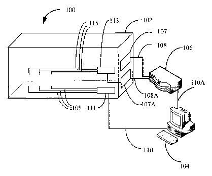
Il s'agit d'un système qui permet de vérifier les communications radio (RF) fournies par un dispositif. Ce système comprend les éléments qui suivent. Une chambre pour isoler le dispositif du brouillage RF; une antenne appropriée aux communications RF avec le dispositif par lequel l'antenne peut assurer les communications dans une certaine gamme de fréquences, ladite antenne étant située à l'intérieur de la chambre; et une liaison de communications numériques pour fournir des communications autres qu'en RF avec le dispositif.


Abrégé anglais

A system for testing radio frequency (RF) communications of a device capable of such communications is provided. The system comprises a chamber for isolating the device from RF interference, an antenna that is suitable for RF communications with the device wherein the antenna is capable of communications over a range of frequencies, the antenna being located within the chamber, and a digital communication link for providing non-RF communications with the device.

Revendications

Note : Les revendications sont présentées dans la langue officielle dans laquelle elles ont été soumises.


What is claimed is:
1. A system for testing radio frequency (RF) communications of a device having
a device
antenna capable of such communications, the system comprising:
a chamber for isolating the device from RF interference;
a chamber antenna for providing RF communications with the device antenna for
an
open air test wherein the chamber antenna is capable of communications over a
range of
frequencies, the chamber antenna being located within the chamber;
a wired RF communication link connectable to an antenna port of the device for
a closed
circuit test;
a digital communication link connectable to the device for providing non-RF
communications with the device; and
a test network for controlling an RF test including the open air test and the
closed circuit
test for the device, the test network communicating with the device through
the digital
communication link, communicating with the chamber antenna for the open air
test, and being
connectable to the device through the wired RF communication link for the
closed circuit test.
2. The system according to claim 1, wherein the test network comprises:
a computer connected to the digital communication link; and
an access point for providing an RF signal for RF communications with the
device, the
chamber antenna being connected to the access point.
3. The system according to claim 1 further comprising:
a jig for holding the device, the jig being located within the chamber and
being moved
therein for RF tuning to determine a desired distance between the chamber
antenna and the
device antenna for the open air test.
4. The system according to claim 1 wherein the chamber antenna is a leaky co-
axial cable.
5. The system according to claim 4 wherein the chamber antenna has an
impedance of
approximately 50 ohms.
6. The system according to claim 4 wherein the chamber antenna is capable of
receiving
an RF communication signal having a frequency between 400 MHz and 3 GHz.
12

7. The system according to claim 1, further comprising:
an attenuator connected to the chamber antenna for attenuating an RF signal to
and
from the device antenna, to a calibrated RF signal level.
8. The system according to claim 1, further comprising:
a first attenuator for the open air test, the first attenuator being connected
to the
chamber antenna for attenuating first RF signal level to and from the device;
and
a second attenuator for the closed circuit test, the second attenuator being
connected to
the wired RF communication link for attenuating second RF signal level to and
from the device.
9. The system according to claim 8, wherein the test network comprises:
an access point communicating with the first attenuator and the second
attenuator for
providing an RF test signal; and
a computer for communicating with the digital communication link and the
access point.
10. The system according to claim 8, wherein the wired RF communication link
comprises:
a splitter for connecting the plurality of devices to the second attenuator.
11. The system according to claim 8, wherein the test network comprises:
means for setting the first attenuator to a calibrated RF communication signal
level;
means for implementing a communication test for the open air test with the
test network;
and
means for verifying that a bit error rate of the device meets a predetermined
RF
performance level.
12. The system according to claim 8, wherein the test network comprises:
means for setting the second attenuator to a calibrated RF communication
signal level;
means for implementing a communication test associated for the closed circuit
test with
the test network; and
means for verifying that a bit error rate of the device a predetermined RF
performance
level.
13

13. The system according to claim 1, further comprising:
a plurality of jigs for holding a plurality of devices, each of the plurality
of devices having
the device antenna and communicating with the digital communication link and
the chamber
antenna, each of the plurality of devices being positioned in the chamber by
the corresponding
jig, depending on RF tuning.
14. The system according to claim 13, wherein the jig is moved for the RF
tuning to
determine a desired distance between the chamber antenna and the device
antenna for the
open air test.
15. The system according to claim 13, further comprising:
a first attenuator for the open air test, the first attenuator being connected
to the
chamber antenna for attenuating first RF signal level to and from the device;
and
a second attenuator for the closed circuit test, the second attenuator being
connected to
the wired RF communication link for attenuating RF signal level to and from
the device.
16. The system according to claim 1, wherein the test network comprises:
means for verifying that the device is in a handshake with the test network.
14

17. A method of testing radio frequency (RF) communications of a device having
a device
antenna capable of the RF communications, the method comprising the steps of:
placing the device in a test chamber for an RF communication test including an
open air
test and a closed circuit test, the chamber including a chamber antenna; and
implementing the RF communication test, including:
setting a first attenuator for the open air test or a second attenuator for
the closed
circuit test, the first attenuator being connected to the chamber antenna for
RF
communications with the device antenna, the second attenuator being
connectable to a
wired communication link for the closed circuit test, the wired communication
link being
connectable to the antenna port of the device antenna;
connecting the device to a test network for controlling the RF communication
test for the
device; and
verifying a bit error rate as an indication of the RF performance of the
device.
18. A method according to claim 17, wherein the device is connectable to the
test network
through the wired communication link.
19. A method according to claim 17, wherein the step of setting comprises:
setting the second attenuator for attenuating a RF signal level to and from
the device.
20. A method according to claim 17, further comprising the step of:
implementing pre-test set up procedure for the open air test, including:
verifying that the device is in a handshake with the test network.
21. A method according to claim 20, wherein the step of implementing pre-test
set up
procedure comprises:
setting the first attenuator to a calibrated RF communication signal level;
and
implementing a communication test with the test network.
22. A method according to claim 18, further comprising the step of:
implementing pre-test set up procedure for the closed circuit test, including:
connecting the device to the closed circuit test RF communication link; and
verifying that the device is in a handshake with the test network.
15

23. A method according to claim 22, wherein the step of implementing pre-test
set up
procedure comprises:
setting the second attenuator to a calibrated RF communication signal level;
and
implementing a communication test with the test network.
24. A method according to claim 17, wherein the step of setting comprises:
setting the first attenuator for attenuating a RF signal level to and from the
device, the
chamber antenna being capable of communications over a range of frequencies.
25. A method according to claim 17, comprising:
verifying that the device is in the RF communication; and
verifying that the device is in a handshake with the test network.
26. A method according to claim 17, comprising:
implementing pre-test set up procedure for the open air test or the closed
circuit test.
27. A method according to claim 26, wherein the step of implementing pre-test
set up
procedure comprises:
calibrating the first attenuator or the second attenuator for the open air
test or the closed
circuit test.
28. A method of testing radio frequency (RF) communications of a device having
a device
antenna capable of the RF communications, the method comprising the steps of:
connecting the device to a test network for controlling a RF communication
test including
an open air test and a closed circuit test in a test chamber; and
implementing pre-test set up procedure for the open air test or the closed
circuit test,
including:
calibrating a first attenuator for the open air test or a second attenuator
for the
closed circuit test, the first attenuator being connectable to the chamber
antenna for the
open air test, the second attenuator being connectable to the device antenna
via a
closed circuit RF communication link for the closed circuit test;
implementing a communication test with the test network; and
verifying a bit error rate as an indication of the RF performance of the
device.
16

29. A method according to claim 28, comprising:
verifying that the device is in the RF communication; and
verifying that the device is in a handshake with the test network.
30. A method according to claim 28, wherein the step of implementing pre-test
set up
procedure comprises:
connecting the device to the closed circuit RF communication link; and
verifying that the device is in a handshake with the test network.
31. A method according to claim 28, comprising:
in the open air test or the closed circuit test, setting the first attenuator
or the second
attenuator to a calibrated RF communication signal level.
32. A method according to claim 28, comprising:
placing the device in a test chamber for an RF communication test including
the open air
test, the closed circuit test and the pre-test set up procedure.
17

Description

Note : Les descriptions sont présentées dans la langue officielle dans laquelle elles ont été soumises.


CA 02531938 2005-12-30
RF Test Chamber
FIELD OF INVENTION
[0001] The invention relates generally to a chamber for testing RF devices,
and more particularly to a chamber that allows for testing over a spectrum of
frequencies.
BACKGROUND OF THE INVENTION
[0002] The testing of RF communication devices requires an environment that
is `free' from RF "interference" that fills many current industrial and or
commercial settings. This interference includes RF signals from wireless
devices including cell phones, pagers, 802.11, RFID devices and Bluetooth
enabled devices to list well-known devices. While the above list is not meant
to be exhaustive it does present common examples of systems that generate
RF signals. Testing is therefore conducted in chambers where the RF device
under test can be isolated from outside interference and thus be protected
from interference from the adjacent electronic devises.
[0003] An outcome of the isolation requirements is that the RF device being
tested will not be able to communicate with antenna located outside of the
chamber i.e. outside of the isolation. Therefore, RF test chambers require an
antenna be incorporated in the chamber.
[0004] Current RF test chambers implement an antenna that is only suitable
for communications over a narrow frequency bandwidth. Further current
antenna designs are only suitable for small test chambers as may be suitable
for the testing of single devices i.e. as in an open-air communication test.
[0005] Therefore, there is a need for an RF test chamber that can
accommodate one or more devices for testing and is capable of testing
devices over numerous frequencies. For example one may wish to test a
device that is capable of communicating using radios that include 802.11, NB
(narrow band), Bluetooth and GSM.

CA 02531938 2005-12-30
SUMMARY OF THE INVENTION
[0006] The present invention relates to a chamber for testing RF
communications devices.
[0007] It is an object of the invention to provide an improved RF device
testing
chamber that mitigates or obviates at least one of the drawbacks of current
test chambers.
[0008] According to an aspect of the invention a system for testing radio
frequency (RF) communications of a device capable of such communications
is provided. The system comprises a chamber for isolating the device from
RF interference, an antenna that is suitable for RF communications with the
device wherein the antenna is capable of communications over a range of
frequencies, the antenna being located within the chamber, and a digital
communication link for providing non-RF communications with the device.
[0009] According to another aspect of the invention use of a leaky coaxial
cable as an antenna in a system for testing RF communications is provided.
The antenna provides RF communications over a range of frequencies.
[0010] Other aspects and advantages of the invention, as well as the structure
and operation of various embodiments of the invention, will become apparent
to those ordinarily skilled in the art upon review of the following
description of
the invention in conjunction with the accompanying drawings.
[0011] This summary of the invention does not necessarily describe all
features of the invention.
BRIEF DESCRIPTION OF THE DRAWINGS
[0012] These and other features of the invention will become more apparent
from the following description in which reference is made to the appended
drawings wherein:
[0013] FIGURE 1 is a schematic diagram of an RF test chamber and test
system, in accordance with an embodiment of the invention;
2

CA 02531938 2005-12-30
[0014] FIGURE 2 is a schematic diagram of the chamber wall panels in
accordance with a further embodiment of the invention;
[0015] FIGURE 3a is a schematic diagram of the cross-section of a chamber
wall panel in accordance with a further embodiment of the invention;
[0016] Figure 3b is a schematic diagram of the cross-section of the chamber
door in accordance with a further embodiment of the invention;
[0017] Figure 3c is a schematic diagram of the cross-section of the chamber
door RF sealing structure in accordance with a further embodiment of the
invention;
[0018] FIGURE 4 is a schematic diagram of the cross-section through the
bottom panel in accordance with a further embodiment of the invention;
[0019] FIGURE 5a is a flow chart of a pre-test set-up procedure for a test
using an internal or integrated antenna in accordance with a further
embodiment of the invention;
[0020] FIGURE 5b is a flow chart of a pre-test set-up procedure for a test
using an external antenna test port in accordance with a further embodiment
of the invention;
[0021] FIGURE 6a is a flow chart of a test procedure for an internal antenna
test in accordance with a further embodiment of the invention; and
[0022] FIGURE 6b is a flow chart of a test procedure for an external antenna
test in accordance with a further embodiment of the invention.
DETAILED DESCRIPTION
[0023] The invention provides a system that is appropriate for testing one or
more multi-band wireless devices.
[0024] The following description is of a preferred embodiment.
[0025] Figure 1 is a block diagram of the testing system 100 of the current
embodiment. The testing system 100 includes a test chamber 102 having
3

CA 02531938 2005-12-30
external dimensions (I/h/d) of 163/ 99/ 87 cm. The test chamber 102 is
designed to accommodate multiple devices (not shown) for RF testing. The
system 100 also includes a computer 104, which controls a given test
(control, monitoring including control of the RF test system and monitoring of
the devices being tested). This includes instructions for the generation of RF
test signals, which are produced by an access point 106. The access point
106 is in-turn connected to variable attenuators 107 and 107A through RF
cables 108 and 108A, respectively. In general all RF cables, including the
cables 108 and 108A, are 50 ohm RGU type cables with a "floating ground".
[0026] The variable attenuators 107 and 107A and their associated circuitry
are for an open and closed circuit RF communication test, respectively. The
attenuators 107 and 107A are passive components in the form of manual
mechanical devices, having two rotary switches for 10 and 1 dB attenuation
settings used to attenuate RF signal level to and from the devise under test.
Attenuation of the attenuators 107 and 107A is set to the calibrated RF signal
level for RSSI minimum communication test specification level.
[0027] The attenuator 107 is connected to chamber antenna 212 and the
attenuator 107A is connected to an eight to one power splitter/combiner 113
for connecting units to a closed circuit system. The splitter 113 is then
connected to an 115 RF cable that is connected to the antenna port of
devices under test during a "closed circuit" test i.e. the chamber antenna is
not used. The devices under test are connected to the computer 104, where
the devices are first connected to a hub 111 with RS232 cables 109 and the
hub 111 is connected to the computer 104 using digital cable 110. The
devices that are being tested are connected to the hub 111.
[0028] Figure 2 is a schematic diagram of the test chamber where the various
panels are shown as if looking at the side of the panel that faces the inside
of
the chamber 102. The back panel 204 has antenna 212 affixed thereto. The
antenna 212 is positioned in the upper half of panel 204. The right-side panel
206 has variable attenuators 107 and 107A affixed to the outside surface
thereof. The bottom panel 210 has test jigs 214 located thereon. In the
current embodiment there are eight test jigs, with three test jigs 214 being
4

CA 02531938 2005-12-30
shown in Figure 2. The test jigs 214 are appropriate for the reception of
devices for testing and are movable on the bottom panel 210. A front panel,
211 includes a door 215 and window 216, where the door 215 provides
access to devices when it is open. The door 215 is attached to the front
panel 211 with hinges (not shown) and opens vertically with the aid of two
pneumatic suspensors (not shown). Finally the door is provided with a lock
system that secures the door in both an open and closed position. The walls
of the chamber could be welded or joined with the proper shaped metal bars.
All sides of the chamber 102 are properly grounded and have a common
ground point, which is connected to the test equipment common ground.
[0029] Details of the panel construction are presented in Figures 3a and 3b
with Figure 3b showing the construction of the front door panel 215. All other
panels are constructed as shown in Figure 3a.
[0030] The panels of the current embodiment are double shielded. The
outermost layer 302 of the panel is a solid aluminum sheet. In an alternative
embodiment this layer may be made of solid steel. A layer of copper mesh
304 is located adjacent to the inside surface of the layer 302. In this
structure
the layers 302 and 304 are connected to a common ground point. A layer of
RF absorber 306 is located adjacent to the insider surface of the layer 304
thereby forming the innermost layer of the panel. The absorber 306 is a
standard absorber that will cover the required frequency range. In the current
embodiment this absorber covers a frequency range that extends from UHF
to 3 GHz. Typically the RF absorbers 306 have dimensions of 60 x 60 x 10
cm each.
[0031] In an alternative embodiment the panels may be single shielded. In
this embodiment the copper shield 304 is not installed. The cooper shield
304 of the door panel is not changed in this embodiment.
[0032] The door panel 215 is shown in Figure 3b. It is a double-shielded
multi-layer structure. A solid aluminum sheet 310 is located on the outside of
the panel. Copper mesh 312 is located adjacent to the sheet 310. RF
absorber 314 is located on the innermost side of the panel. Layer 316 is an
5

CA 02531938 2005-12-30
optional metal plate that may be used in an alternative embodiment to ensure
placement of the RF absorber.
[0033] The door 215 must also be provided with an RF "seal". The structure
used for this seal is depicted in Figure 3c. An "L" shaped metal bar 320 is
fitted around the inside of the door 215. A "U" shaped metal structure 322 is
around the front panel 216 such that the "L" bar 320 fits therein when the
door
215 is closed. Another element of the RF seal is copper ground 'fingers' 324
that are located within the structure 322. As depicted in Figure 3c the ground
fingers 324 fit snugly about the rod 320 when it is lowered into the structure
322. A ground contact is thereby made with the door 215 and an RF seal is
formed.
[0034] Figure 4 presents a section through the bottom panel illustrating the
solid metal panel 302, the copper mesh 304 and the RF absorbers 306.
Three device holders 214 are shown on top of the RF absorber 306 of the
bottom panel structure. The device holders 214 may also be referred to as
jigs 214. Devices to be tested 404 are inserted into the jigs 214.
[0035] The devices 404 have an internal antenna (not shown). This internal
antenna may be on a separate printed circuit board on the same printed
circuit board as the PC card (not shown) on which the radio is located. If the
antenna is separate from the radio card it is connected thereto using an RF
cable. In an "open-air" test the internal antenna will communicate with the
chamber antenna 212. During a closed circuit test the devices 404 will be
connected to the access point 106 via RF cables 115 that are connected to
the devices 404 via the antenna access point 406.
[0036] When the devices 404 are inserted in the jigs 214 they are connected
to and in data communication with the test PC 104 via RS232 cables 109,
which are connected to the test jigs 214. This digital connection is present
when during both the open air and closed circuit test.
Antenna
[0037] A central aspect of the current embodiment is the antenna 212. The
antenna 212 provides RF coverage for the chamber 102 over a range of
6

CA 02531938 2005-12-30
frequencies. The antenna 212 is a 50 Ohm leaky coaxial cable. In the
current embodiment a FlexRadTM-600 flexible low loss communication Coax
is used as a Short Antenna feeder run. Other similar antenna that provide for
similar operation will be apparent to those of skill in the art. The antenna
212
offers broadband performance up to 3 GHz. In the current embodiment the
antenna 212 provides for RF coverage between about 400 MHz and about 3
GHz.
[0038] As illustrated in Figure 2 the antenna 212 is in the form of a straight
line and is placed on the back panel 204 of the test chamber 102. The
io antenna 212 of the current embodiment has a length that is equal to the
length of the chamber 102 i.e. length of the rear panel 204. Without being
limited by theory it is currently understood that the minimum length of the
antenna 212 is equal to a fraction of the wavelength of the lowest frequency
of the test. Further, the antenna 212 is positioned within the chamber 102
is such that the distance between the antenna 212 and the device antenna 406
is at least equal to a function of the highest and lowest chamber operating
frequency wavelength.
[0039] The RF coverage can be improved through RF tuning of the antenna
212. In the current embodiment tuning is accomplished by repositioning the
20 device 404 within the test chamber 102. The repositioning may include
vertical movement of the device 404 in the jig 214 in which it is inserted or
horizontal movement of the jig 214 within the chamber 102. This tuning will
thereby provide for the desired distance between the antenna 212 and the
device antenna 406.
25 Operation
[0040] It is an object of the invention to provide an integrated test
environment
where a device can be tested in both a closed circuit and open-air
environment over a variety of frequencies. Further the tests can be
performed without having to remove the device 404 from the test chamber
30 102. This therefore provides for a simplified testing procedure. A closed
circuit test might test for parameters including modulation, conducted
7

CA 02531938 2005-12-30
spurious and receiver sensitivity. Other parameters that might be tested in a
closed circuit test will be apparent to those of skill in the art. Testing of
these
parameters is a common way of verifying the operation of a device 404
without using the device antenna 406. Further use of closed circuit testing
allows the reduction of interference so these parameters are tested under a
controlled testing condition.
[0041 ] The operation of the device antenna 406 radiated test parameters that
could not be tested in a closed circuit test can be tested by means of an
open-air test. In such a test the device antenna 406 communicates with the
io chamber antenna 212, which in-turn is connected to the access point 106.
[0042] Figures 5a and 5b present flow charts of the pre-test set-up procedure
to be carried out for an open air and closed circuit test, respectively.
[0043] With regard to Figure 5a any assembly of devices is performed and the
devices are configured for a communication test at step 502. At step 504 the
1s devices to be tested 404 are placed in the jigs 214 of the test chamber 102
and the devices 404 are turned on. With the device power on the devices
404 attempt to communicate with the RF host or access point 106 using an
open-air coupling i.e. via antenna 212. At step 508 it is verified that the
devices 404 are in a "handshake" configuration with regard to the access
20 point 106. Data from the devices 404 that is associated with the bench set-
up
in the test chamber 102, prior to a test, is saved to the PC 104 using the
RS232 data lines 109. At step 510 the operator may verify proper operation
of the devices 404. At step 512 the variable attenuator 107 is set to the
calibrated RF communication Signal level. This is an important step in
25 assuring a proper communication test. At step 514 the test process is
initiated at the PC 104 and the Received RF Signal Strength (RSSI) is read
for each unit 404. Step 514 assists in detecting a non-operational unit prior
to
the communication test. The above communication test is operated through
the RS232 data lines 109 and it is determined whether the device received
30 the RF signal. Software on the PC 104 will run the communication test with
each assigned device being tested and, through the data line 109, read the
RF signal value (RSSI) at the device being tested 404.
8

CA 02531938 2009-11-26
[0044] The chamber door 215 is dosed at step 510 and the system is left to
"set in the cellular test mode. At step 518 the Bit Error Rate (BER) % is
verified for the minimum test communication packages. The BER% Is the
statistic read from the access point 106 and is an indication of the RF
performance In the chamber 102. If the device 404 does not pass the BER%
at this point it is rejected.
[0045] The pre-test procedure fora dosed circult test outlined in Figure 5b is
quite similar to that of a open-air test outlined in Figure 5a. There are
however two differences due to this being a dosed circuit test. At step 532
io the RF cables 115 are connected to the devices 404 that are to be tested.
At
step 534 the devices 404 try to communicate with the access point 106 using
the RF cable 109.
(0046] Once the device has been set-up as per the methods outlined in Figure
5A and 58 the actual RF communication test can be performed. The method
is of performing an open-air test according to an embodiment of the Invention
is
presented in Figure 6A. Al step 602 RF the test chamber 102 and devices
404 are connected as outlined in Figures 1 and 4. The variable attenuator
107 is calibrated to the open-air dB level at step 804. At step 606 the PC 104
and access point 106 are set for an RF communication test. At step 608 the
20 RS232 cable is connected to the jigs 214 in the chamber 1.02. The devices
404 are Inserted into the appropriate jig 214 and turned on at step 610. At
step 612 all of the devices are assigned to the test network i.e. the access
point 106 and the PC 104. Versification that the devices 404 are In RF and
digital communications is performed at step 614. At step 616 the test
25 program on PC 104 is imitated such that the device operation is visible on
PC
104. It RF interference Is noted during monitoring of the BER% and the test
data the chamber door 215 is dosed at step 618. At step 620 the testis
stopped after completion thereof or if the test data indicates the test should
be stopped.
30 [0047] The test procedure for a closed circuit test is outlined in Figure
6b. The
procedure is generally the same as that outlined in Figure 6a. However at
step 632 the variable attenuator 107A is calibrated for the closed circuit dB
9

CA 02531938 2005-12-30
level. At step 634 the PC 104 and the access point 106 are set for a closed
circuit RF communication test.
Sample Test Data
[0048] The following test data was measured for a typical open-air
communication test as per the embodiments of the invention. Attenuation
due to Rf interference i.e. ambient' RF exposure was measured up to -85 dB,
which is the limit of the test equipment used. Further the VSWR was
measured at 1:17. It is noted that all of the above RF measurements were
made in the 'working' test areas with a surrounding `live' RF test and
io communication on all ranges of frequencies (from UHF to 2.5 GHz).
[0049] Table 1 presents measurements of the RSSI of a hand held computer
that was tested in accordance with an embodiment of the invention. The
internal antenna was operating in the 2.4 GHz operating bandwidth when the
data of Table 1 was collected.
[0050] Table 1
802.11 UUT:RSS per socket (-dBm)
CH# 1 2 3 4 5 6 aver
6 76 79 78 79 78 78
13 78 79 76 79 76 77.6
[0051] In an alternative embodiment the shape of antenna 212 could be an
"S" shape and is installed on a side or upper panel of the chamber 102 as per
calibration requirements. The positioning of the antenna 212 is a function of
the device geometry and device anten406 whereby the positioning ensures
that there is communication between the device antenna 406 and the
antenna 212.

CA 02531938 2005-12-30
[0052] While the invention has been described according to what is presently
considered to be the most practical and preferred embodiments, it must be
understood that the invention is not limited to the disclosed embodiments.
Those ordinarily skilled in the art will understand that various modifications
and equivalent structures and functions may be made without departing from
the spirit and scope of the invention as defined in the claims. Therefore, the
invention as defined in the claims must be accorded the broadest possible
interpretation so as to encompass all such modifications and equivalent
structures and functions.
11

Dessin représentatif
Une figure unique qui représente un dessin illustrant l'invention.
États administratifs

2024-08-01 : Dans le cadre de la transition vers les Brevets de nouvelle génération (BNG), la base de données sur les brevets canadiens (BDBC) contient désormais un Historique d'événement plus détaillé, qui reproduit le Journal des événements de notre nouvelle solution interne.

Veuillez noter que les événements débutant par « Inactive : » se réfèrent à des événements qui ne sont plus utilisés dans notre nouvelle solution interne.

Pour une meilleure compréhension de l'état de la demande ou brevet qui figure sur cette page, la rubrique Mise en garde , et les descriptions de Brevet , Historique d'événement , Taxes périodiques et Historique des paiements devraient être consultées.

Historique d'événement

Description Date
Représentant commun nommé 2019-10-30
Exigences relatives à la nomination d'un agent - jugée conforme 2012-05-14
Inactive : Lettre officielle 2012-05-14
Lettre envoyée 2012-05-14
Inactive : Lettre officielle 2012-05-14
Exigences relatives à la révocation de la nomination d'un agent - jugée conforme 2012-05-14
Demande visant la révocation de la nomination d'un agent 2012-04-25
Inactive : Transfert individuel 2012-04-25
Demande visant la nomination d'un agent 2012-04-25
Accordé par délivrance 2011-10-18
Inactive : Page couverture publiée 2011-10-17
Inactive : Lettre officielle 2011-09-15
Exigences relatives à la nomination d'un agent - jugée conforme 2011-08-23
Inactive : Lettre officielle 2011-08-23
Exigences relatives à la révocation de la nomination d'un agent - jugée conforme 2011-08-23
Exigences relatives à la nomination d'un agent - jugée conforme 2011-08-23
Exigences relatives à la révocation de la nomination d'un agent - jugée conforme 2011-08-23
Demande visant la révocation de la nomination d'un agent 2011-08-16
Demande visant la nomination d'un agent 2011-08-16
Inactive : Lettre officielle 2011-08-15
Un avis d'acceptation est envoyé 2011-08-15
Inactive : CIB désactivée 2011-07-29
Inactive : Approuvée aux fins d'acceptation (AFA) 2011-07-25
Lettre envoyée 2011-07-13
Exigences de rétablissement - réputé conforme pour tous les motifs d'abandon 2011-06-27
Retirer de l'acceptation 2011-06-23
Requête en rétablissement reçue 2011-06-23
Inactive : Taxe finale reçue 2011-06-23
Taxe finale payée et demande rétablie 2011-06-23
Préoctroi 2011-06-23
Modification reçue - modification volontaire 2011-06-23
Réputée abandonnée - omission de répondre à un avis sur les taxes pour le maintien en état 2010-12-30
Réputée abandonnée - les conditions pour l'octroi - jugée non conforme 2010-10-01
Un avis d'acceptation est envoyé 2010-04-01
Lettre envoyée 2010-04-01
month 2010-04-01
Un avis d'acceptation est envoyé 2010-04-01
Inactive : Approuvée aux fins d'acceptation (AFA) 2010-03-22
Modification reçue - modification volontaire 2009-11-26
Inactive : CIB attribuée 2009-07-09
Inactive : CIB en 1re position 2009-07-09
Inactive : CIB enlevée 2009-07-09
Inactive : Dem. de l'examinateur par.30(2) Règles 2009-07-06
Inactive : CIB expirée 2009-01-01
Demande publiée (accessible au public) 2007-06-30
Inactive : Page couverture publiée 2007-06-29
Inactive : CIB en 1re position 2006-09-05
Inactive : CIB attribuée 2006-09-05
Inactive : CIB attribuée 2006-09-03
Lettre envoyée 2006-08-11
Lettre envoyée 2006-03-27
Inactive : Transfert individuel 2006-02-17
Inactive : Lettre de courtoisie - Preuve 2006-02-14
Inactive : Certificat de dépôt - Sans RE (Anglais) 2006-02-08
Demande reçue - nationale ordinaire 2006-02-07
Toutes les exigences pour l'examen - jugée conforme 2006-01-03
Exigences pour une requête d'examen - jugée conforme 2006-01-03
Requête d'examen reçue 2006-01-03

Historique d'abandonnement

Date d'abandonnement Raison Date de rétablissement
2011-06-23
2010-12-30
2010-10-01

Taxes périodiques

Le dernier paiement a été reçu le 2011-08-16

Avis : Si le paiement en totalité n'a pas été reçu au plus tard à la date indiquée, une taxe supplémentaire peut être imposée, soit une des taxes suivantes :

  • taxe de rétablissement ;
  • taxe pour paiement en souffrance ; ou
  • taxe additionnelle pour le renversement d'une péremption réputée.

Les taxes sur les brevets sont ajustées au 1er janvier de chaque année. Les montants ci-dessus sont les montants actuels s'ils sont reçus au plus tard le 31 décembre de l'année en cours.
Veuillez vous référer à la page web des taxes sur les brevets de l'OPIC pour voir tous les montants actuels des taxes.

Titulaires au dossier

Les titulaires actuels et antérieures au dossier sont affichés en ordre alphabétique.

Titulaires actuels au dossier
PSION INC.
Titulaires antérieures au dossier
ZIVOTA ZEKE STOJCEVIC
Les propriétaires antérieurs qui ne figurent pas dans la liste des « Propriétaires au dossier » apparaîtront dans d'autres documents au dossier.
Documents

Pour visionner les fichiers sélectionnés, entrer le code reCAPTCHA :


Pour visualiser une image, cliquer sur un lien dans la colonne description du document (Temporairement non-disponible). Pour télécharger l'image (les images), cliquer l'une ou plusieurs cases à cocher dans la première colonne et ensuite cliquer sur le bouton "Télécharger sélection en format PDF (archive Zip)" ou le bouton "Télécharger sélection (en un fichier PDF fusionné)".

Liste des documents de brevet publiés et non publiés sur la BDBC .

Si vous avez des difficultés à accéder au contenu, veuillez communiquer avec le Centre de services à la clientèle au 1-866-997-1936, ou envoyer un courriel au Centre de service à la clientèle de l'OPIC.

({010=Tous les documents, 020=Au moment du dépôt, 030=Au moment de la mise à la disponibilité du public, 040=À la délivrance, 050=Examen, 060=Correspondance reçue, 070=Divers, 080=Correspondance envoyée, 090=Paiement})


Description du
Document 
Date
(aaaa-mm-jj) 
Nombre de pages   Taille de l'image (Ko) 
Description 2005-12-29 11 455
Abrégé 2005-12-29 1 12
Revendications 2005-12-29 2 50
Dessin représentatif 2007-06-25 1 19
Revendications 2009-11-25 3 106
Description 2009-11-25 11 462
Revendications 2011-06-22 6 206
Dessin représentatif 2011-09-26 1 20
Dessins 2009-11-25 8 189
Certificat de dépôt (anglais) 2006-02-07 1 158
Courtoisie - Certificat d'enregistrement (document(s) connexe(s)) 2006-03-26 1 128
Accusé de réception de la requête d'examen 2006-08-10 1 177
Rappel de taxe de maintien due 2007-09-03 1 112
Avis du commissaire - Demande jugée acceptable 2010-03-31 1 166
Courtoisie - Lettre d'abandon (AA) 2010-12-28 1 165
Courtoisie - Lettre d'abandon (taxe de maintien en état) 2011-02-23 1 173
Avis de retablissement 2011-07-12 1 172
Courtoisie - Certificat d'enregistrement (document(s) connexe(s)) 2012-05-13 1 104
Correspondance 2006-02-07 1 26
Taxes 2007-12-12 1 38
Taxes 2008-12-15 1 40
Taxes 2009-12-15 1 39
Correspondance 2011-06-22 2 71
Correspondance 2011-08-14 1 17
Taxes 2011-08-15 2 132
Correspondance 2011-08-15 3 160
Correspondance 2011-08-22 1 14
Correspondance 2011-08-22 1 17
Correspondance 2011-09-14 1 14
Correspondance 2011-09-14 1 18
Correspondance 2012-04-24 7 223
Correspondance 2012-04-24 11 369
Correspondance 2012-05-13 1 14
Correspondance 2012-05-13 1 16