Note : Les descriptions sont présentées dans la langue officielle dans laquelle elles ont été soumises.
. CA 02533498 2011-09-20
1
TITLE OF THE INVENTION
[001] MODULATED TRIANGULAR WAVE-AMPLIFIER
[002]
TECHNICAL FIELD OF INVENTION =
[003] The present invention relates to amplifier design, and more
particularly to a
power amplifier for audio and other signals. Still more specifically, the
present
invention relates to design Of an amplifier circuit capable of manipulating an
unregulated AC signal to provide an amplified signal to a load device, so that
fluctuations in the power supply to the amplifier circuit are compensated for,
and
noise or ripples present in the power supply are removed, eliminating the
requirement for a regulated power supply.
BACKGROUND OF THE INVENTION
[004] Power amplifiers are commonly used to amplify electrical signals
supplying
power to certain types of electronic devices, such as audio speakers. Most
power amplifiers use, and depend upon, clean, regulated direct current (DC)
power input. Unregulated DC power generated from unregulated alternating
current (AC) is "noisy", containing power fluctuations unsuitable for most
power
amplifying applications.
[005] In typical applications, power amplifiers must convert an
unregulated, noisy
120-volt AC power source into a regulated, clean DC power source. If the
unregulated AC power input is simply rectified to a DC power input, .any
fluctuations, noise or ripple in the AC power signal may be transferred to the
DC
power signal. The noise inherent in DC power in this situation may be
translated to the amplified output signal. In audio applications, such
excessive
variances in the power supply will result in undesirable hum, distortions, and
noise at the speaker. As such, there is a need for regulated DC power supplies
to power applications with a reduced noise factor.
CA 02533498 2006-01-23
WO 2005/011105 PCT/US2004/024020
2
[006] Conventional power amplifiers rectify an AC signal to a regulated DC
power
source with transformers and other active inductive and capacitive circuits,
which account for the majority of the weight, waste heat output, and cost of
production associated with these prior-art amplifiers. As such, there is also
a
need for audio amplifiers that weigh less, produce less heat, and cost less.
[007] A number of approaches have been tried to minimize or overcome the
above-
identified problems. U.S. Patent 4,042,890 to Eckerie filters the DC power
signal to reduce high-frequency noise. U.S.
Patent 4,605,910 to Covill
produces a switch modulated signal for producing an output signal that is
independent of the supply voltage, thereby eliminating noise caused by
fluctuating AC voltage signals. U.S. Patent 4,737,731 to Swanson senses
variations in the DC power signal and adjusts the gain in the audio frequency
signal according to the variances to reduce modulation distortion. In U.S.
Patent 5,132,637 also to Swanson, a plurality of actuable power amplifiers are
controlled by a correction signal to produce a cleaner signal. U.S. Patent,
5,777,519 to Simopoulos uses a correction signal as an input to a variable
switching power supply to eliminate some noise in the power signal.
[008] However, each of these methods share the problems of high cost, high
heat
loss, high weight, and overall inefficiency. A different method for regulating
the
power output that eliminates the regulated DC power source would offer
significant advantages in cost and efficiency as well as a significant
reduction in
weight and increase in output power.
SUMMARY OF THE INVENTION
[009] The present invention eliminates the need to regulate a DC power
supply by
regulating the gain of an amplifier in response to fluctuations and ripple in
the
unregulated DC power supply so that those fluctuations and ripples do not
appear at the output power signal. Unregulated AC power may be supplied
from a conventional AC outlet or from an isolation or other transformer.
Unregulated AC power is first rectified into unregulated DC power, and this
unregulated DC power signal is monitored by a voltage divider to establish a
power supply "variance" signal. This variance signal is then squared by an
analog multiplier. A second multiplier processes the signal from the first
multiplier with a triangular wave signal to produce, an input signal to an
internal
CA 02533498 2011-09-20
3
comparator. The first and second voltage multipliers comprise a triangular
wave modulator. The resulting output signal from the second multiplier is the
modulated triangular wave signal.
[0010] An internal comparator accepts an input audio signal as well as the
output
signal from the second multiplier. This internal comparator monitors and
processes the input audio signal with the modulated triangular wave signal to
generate a Pulse Width Modulation (PWM) output signal. From the internal
comparator, the PWM output signal is amplified by power device transistors,
and the amplified PWM signal passes through filters to remove a high
frequency carrier component. The signal output from the filters is an
amplified
PWM power signal, which is then used to drive a load device.
[0011] The variances in the power supply voltage are demodulated or removed
by this
approach, thereby eliminating the need for a regulated DC power supply. The
invention provides for dynamic adjustment for noise in the unregulated DC
power supply, resulting in a simpler and more efficient power amplifier to
derive
a clean, regulated, amplified power drive signal. The present invention also
provides audio improvements including compression and frequency
equalization.
BRIEF DESCRIPTION OF THE DRAWINGS
[0012] The aspects and features of the invention will become more readily
understood
from the following detailed description and appended claims when read in
conjunction with the accompanying drawings in which like- numerals represent
like elements.
[0013] Fig. 1 is a basic circuit block diagram illustrating a preferred
embodiment of the
functional components of the power amplifier of the present invention.
[0014] Fig. 2 is a circuit schematic of a preferred embodiment of the AC
power circuit.
[0015] Fig. 3 is the circuit schematic of a preferred embodiment of the DC
bridge
rectifier and voltage divider.
CA 02533498 2006-01-23
WO 2005/011105 PCT/US2004/024020
4
[0016] Fig. 4 is a circuit schematic of a preferred embodiment of the
triangular wave
modulator (TVVM) containing two voltage multipliers.
[0017] Fig. 5 is a circuit schematic of a preferred embodiment of the pulse
width
modulator (PWM) controller containing the triangular wave generator and pulse
width modulation amplifier.
[0018] Fig. 6 is the circuit schematic of a preferred embodiment of the
power device
transistor and filter.
[0019] Fig. 7 is a circuit schematic of a preferred embodiment of the RMS-
to-DC
converter used to provide an additional signal for providing dynamic range
compression, or Automatic Gain Control, to the amplifier circuit.
[0020] Fig. 8 is a composite circuit schematic of a preferred embodiment of
the present
invention for a modulated triangular wave audio power amplifier.
[0021] Fig. 9 illustrates the internal operative connectivity for the PWM
controller
illustrated schematically and described in detail in connection with FIG. 5.
[0022] Fig. 10 is a block diagram of the modulated triangular wave audio
power
amplifier configured as a noise-canceling amplifier.
[0023] Fig. 11 is a block diagram of the modulated triangular wave audio
power
amplifier configured to compress or expand dynamic range or for signal
equalization or cancellation.
[0024] Fig. 12 is a block diagram of the modulated triangular wave audio
power
amplifier configured to introduce an additional signal to output.
DETAILED DESCRIPTION OF THE PREFERRED EMBODIMENTS
[0025] In the following Detailed Description of the Preferred Embodiments,
reference is
made to the accompanying drawings which form a part hereof, and in which are
shown by way of illustration specific embodiments in which the invention may
be practiced. It is to be understood that other embodiments may be utilized
and
structural changes may be made without departing from the scope of the
CA 02533498 2006-01-23
WO 2005/011105 PCT/US2004/024020
present invention. For example, intervening electrical components may be
located along electrical connections, and electrical components of different
ratings may be used, without departing from the scope of the present
invention.
Moreover, persons of ordinary skill in the art will know that numerous minor
alternatives to a specific circuit design are possible, without departing from
the
scope of the present invention. Thus understood, the details of the circuit
provided, including the ratings of the electrical components in the specific
preferred embodiments, are not intended to limit the scope of any claim, nor
to
be read into any claim, but merely to provide an example of a fully enabled
and
disclosed best mode of practicing a preferred embodiment of the invention.
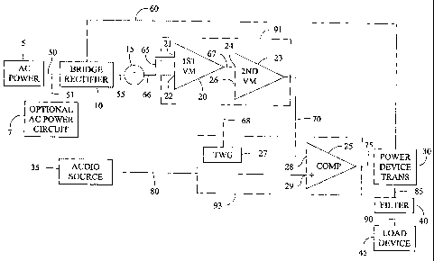
[0026] FIG. 1
illustrates a preferred embodiment of the basic electrical components of
the amplifier of the present invention. As seen in FIG. 1, an AC power supply
5
is coupled to an optional AC power circuit (transformer) 7 by an electrical
connection 50. Optional AC power circuit 7 is coupled to a bridge rectifier 10
by
an electrical connection 51. Bridge rectifier 10 is coupled to a voltage
divider 15
by an electrical connection 55. Bridge rectifier 10 is also coupled to a power
device transistor 30 by an electrical connection 60.
[0027]
Voltage divider 15 is coupled to a first input 21 of a first voltage
multiplier 20 by
an electrical connection 65 and to a second input 22 by an electrical
connection
66. The output of first voltage multiplier 20 is coupled to a first input 24,
of a
second voltage multiplier 23 by an electrical connection 67. A triangular wave
generator 27 is coupled to a second input 26 of second voltage multiplier 23
by
electrical connection 68. First voltage multiplier 20 and second voltage
multiplier 23 comprise a triangular wave modulator (TVVM) 91.
[0028] The
output of second voltage multiplier 23 is coupled to a first input 28 of an
internal comparator 25 by an electrical connection 70. In a
preferred
embodiment, an audio signal source 35 is coupled to a second input 29 of an
internal comparator 25 by an electrical connection 80. The output of internal
comparator 25 is coupled to a power device transistor 30 by an electrical
connection 75. In the preferred embodiment, internal comparator 25 is internal
of a pulse width modulation controller integrated circuit (PWM controller 93)
that
includes triangular wave generator 27, as described in detail below. Power
CA 02533498 2006-01-23
WO 2005/011105 PCT/US2004/024020
6
device transistor 30 is coupled to a filter 40 by an electrical connection 85.
Filter 40 is coupled to a load device 45 by an electrical connection 90.
[0029] In operation, unregulated AC power supply 5 supplies an unregulated,
AC
power signal to the amplifier. The unregulated AC power signal passes through
bridge rectifier 10, which rectifies, or converts, the unregulated AC power
signal
into an unregulated DC power signal. This unregulated DC power signal is
used to provide a reference voltage to triangle wave modulator 91 as well as
being used by power device transistors 30 to power load device 45.
[0030] From bridge rectifier 10, the unregulated DC power signal passes
through
voltage divider 15. Voltage divider 15 establishes a unity voltage level and
provides two input power signals comprising the voltage variance of the power
signal into first voltage multiplier 20. First voltage multiplier 20
multiplies these
two signals together, providing an unregulated DC power signal equal to the
square of the voltage variance.
[0031] The output of first voltage multiplier 20 is coupled to first input
24 of second
voltage multiplier 23. Triangular wave generator 27 generates a triangular
wave
signal that is coupled to second input 26 of second voltage multiplier 23.
These
two signals are multiplied together by second voltage multiplier 23 to
generate a
modulated triangular wave signal.
[0032] The modulated triangular wave signal, output from triangular wave
modulator
91, is the first input to PWM Amp 25. The second input to PWM Amp 25 is the
audio signal being amplified, from audio source 35. PWM Amp 25 compares
the modulated triangular wave signal and the audio signal to generate a pulse
width modulation (PWM) power signal carrying the audio component. The
PWM power signal then passes to power device transistors 30, which amplify
the PWM power signal. This amplified PWM power signal then passes through
filter 40 (e.g., an inductance capacitor filter) which filters out the high-
frequency
carrier component of the PWM power signal. This filtered PWM power signal
provides a clean, undistorted audio signal free of noise to load device 45
because the modulated triangle wave signal compensates for variances in AC
power supply 5, powering the load device 45 for the relevant application.
CA 02533498 2006-01-23
WO 2005/011105
PCT/US2004/024020
7
[0033] FIG. 2 illustrates a preferred embodiment for the AC power circuit
(7 in FIG. 1)
of the present invention. In this embodiment, the AC power circuit uses a
triac
150 and optocoupler 140 to delay the onset of AC power in the amplifier. This
time delay power-on circuit delays the onset of AC power to allow the control
circuit to stabilize and avoid loud pops when switched on.
[0034] In the circuit, AC power from an outside AC power source (e.g., wall
outlet,
generator, etc.) is provided through an electrical pole 101 and an electrical
pole
103. Electrical poles 101 and 103 are coupled respectively by an electrical
connection 102 and an electrical connection 104 in a parallel electrical
circuit
with a two-pole circuit breaker 105. Electrical connection 102 is coupled from
circuit breaker 105 to a transformer 110 (e.g., 12-volt transformer).
Electrical
connection 104 is also coupled from circuit breaker 105 to transformer 110.
[0035] Transformer 110 steps down the supply voltage (e.g., from 120-volts
AC to 12-
volts AC). Current flows from transformer 110 through two electrical
connections 111 and 113 to a bridge rectifier 112. The output from bridge
rectifier 112 passes through electrical connections 116 and 114 to a filter
network 115. In a specific preferred embodiment, filter network 115 comprises
a 2200 pF capacitor 117, a 100 pF capacitor 118, and a .1 pF capacitor 119
coupled in parallel with bridge rectifier 112 by electrical connections 116
and
114.
[0036] An electrical connection 121 couples a power supply regulator 120 to
electrical
connection 116. In a specific preferred embodiment, power supply regulator
120 is of the type comparable to a Motorola 78L12. Power supply regulator 120
is coupled to an electrical ground 108 by an electrical connection 123. A
capacitor 124 and a capacitor 126 are coupled to power supply regulator 120 by
an electrical connection 122. The two capacitors 124 and 126 are also coupled
together by electrical connection 114.
[0037] An electrical connection 127 couples a resistor 128 to a terminal
V12 125.
Terminal V12 125 represents a source of direct current (DC) power supplied for
the circuit. In the preferred embodiment disclosed, the voltage supplied is
for a
12-volt circuit. Also in the preferred embodiment disclosed, resistor 128 is a
CA 02533498 2006-01-23
WO 2005/011105 PCT/US2004/024020
8
68K-ohm resistor. A resistor 129 is coupled to electrical connection 127 by an
electrical connection 130 in a parallel electric circuit configuration.
[0038] As stated, terminal V12 125 is coupled to electrical connection 127,
and this
electric terminal V12 125 provides a DC power source (e.g., 12-volt). Resistor
128 and resistor 129 are both coupled to the DC power source. Resistor 128 is
coupled in series with another resistor 131 by electrical connection 133. In a
specific preferred embodiment, resistor 131 is a 68K-ohm resistor. Resistor
129
is coupled in series with a capacitor 132 by an electrical connection 134.
Resistor 131 is coupled to an electrical ground 108 by an electrical
connection
136, and capacitor 132 is coupled to an electrical ground 108 by an electrical
connection 137.
[0039] A comparator 135 is coupled to electrical connections 133 and 134.
The non-
inverting input to comparator 135 is coupled to electrical connection 134 by
an
electrical connection 139. The inverting input of comparator 135 is coupled to
electrical connection 133 by an electrical connection 141. Comparator 135
compares the input voltages of the two electrical connections. If the voltage
at
electrical connection 139 is less than the voltage at electrical connection
141,
the output of comparator 135 will be low, with the voltage at the output at an
electrical connection 142 at the lowest possible value (e.g., digital output =
0).
If the voltage at electrical connection 139 is greater than the voltage at
electrical
connection 141, the output of comparator 135 will be high, with the voltage at
the output at electrical connection 142 at its highest value (e.g., digital
output =
1).
[0040] An optocoupler 140 is comprised of a light emitting diode (LED) 171
and a
phototransistor 172 inside a component case. Light emitting diode 171 emits
light when the digital output value from comparator 135 equals 1 (e.g., the
voltage at electrical connection 139 is greater than that at electrical
connection
141). An electrical connection 143 couples a resistor 144 to the LED 171. An
electrical connection 146 couples resistor 144 to ground 108. In a specific
preferred embodiment, resistor 144 is a 560K-ohm resistor.
[0041] Phototransistor 172 has a light sensitive base region. When light
strikes the
photosensitive base of phototransistor 172, the emitter-to-collector
resistance
CA 02533498 2006-01-23
WO 2005/011105 PCT/US2004/024020
9
falls, allowing current to flow through phototransistor 172. When the digital
output value from comparator 135 equals 1 (logic 1 state), LED 171 is
illuminated. Light from LED 171 charges the base of phototransistor 172,
permitting current flow through phototransistor 172. Thus, optocoupler 140
functions as a switch triggered by the output of comparator 135.
[0042] An
electrical connection 152 couples circuit breaker 105 and the AC power to a
capacitor 157, a triode alternating current switch (triac) 150, and a resistor
145.
Resistor 145 is coupled to optocoupler 140 by an electrical connection 147. An
electrical connection 149 further couples electrical connection 147 to the
gate of
triac 150. Triac 150 is coupled to a terminal L2165 and optocoupler 140 by an
electrical connection 151. Capacitor 157 is coupled to a resistor 155 by an
electrical connection 156, and resistor 155 is further coupled to terminal L2
165
by an electrical connection 153. Terminal L1160 is coupled to transformer 110
and breaker 105 by electrical connection 107.
[0043] Optocoupler 140 isolates triac 150 from the control circuit. When
phototransistor 172 is activated by LED 171, voltage applied to the gate of
triac
150 causes current to flow through triac 150 and energize terminal L2 165.
Once the gate activates triac 150, AC power will continue to terminal L2 165
and
L1 160 as long as the circuit remains energized. The optocoupler 140 and triac
150 combination will delay circuit power-up until the control circuit
stabilizes,
avoiding pops and hiss from the audio output.
[0044] FIG. 3
illustrates a preferred embodiment of a bridge rectifier 205 (10 in FIG. 1)
and a voltage divider (resistors 210, 215, and their electrical
interconnection, 15
in FIG. 1) of the present invention. A pair of terminals L1 160 and L2 165 are
coupled to bridge rectifier 205 by electrical connections 201 and 202
respectively. Two electrical output connections from bridge rectifier 205
couple
to a resistor-capacitor (RC) filter and resistor voltage divider network
arrangement. An electrical connection 208 couples bridge rectifier 205 to
terminal VA 240. Terminal VA 240 represents a high voltage terminal
connection. An electrical connection 207 couples bridge rectifier 205 to an
electrical connection 221, and to an electrical connection 206. Electrical
connection 221 is coupled to ground 108. An electrical connection 209 couples
bridge rectifier 205 to a capacitor 230. In a specific preferred embodiment,
CA 02533498 2006-01-23
WO 2005/011105 PCT/US2004/024020
capacitor 230 is a 1000 pF capacitor. Electrical connection 206 couples
capacitor 230 to electrical connection 207. Electrical connection 209 is also
coupled to electrical connection 208.
[0045] A resistor 210 and a resistor 215 are connected in series to each
other and to
capacitor 230 in a parallel circuit. An electrical connection 212 couples
resistor
210 to electrical connection 208. An electrical connection 211 further couples
resistor 210 to resistor 215. Electrical connection 221 couples resistor 215
to
ground 108.
[0046] An electrical connection 213 couples resistors 210 and 215 to the
non-inverting
terminal of an operational amplifier 218 (op amp 218). An electrical
connection
217 couples the output of op amp 218 to the inverting terminal input of op amp
218. Thus configured op amp 218 performs as a voltage follower. An electrical
connection 216 connects the output of op amp 218 (the voltage follower) to a
terminal T1 250. The arrangement of the resistors 210 and 215 and the
electrical connections 213 and 211 between resistors 210 and 215 comprises a
resistor voltage divider network. One or both of resistors 210 and 215 may be
variable, to accommodate adjustment of the power variance signal.
[0047] FIG. 4 illustrates a preferred embodiment of the circuit for the
triangular wave
modulator (91 in FIG. 1) of the present invention. Although the preferred
embodiment shown in FIG. 4 discloses a design for an analog circuit, the
equivalent functionality may be achieved through digital circuitry, such as,
for
example, by use of digital signal processors.
[0048] As seen in FIG. 4, a terminal T1 250 is coupled to a first resistor
382 by an
electrical connection 301. Resistor 382 is subsequently coupled to a first
voltage multiplier 310 (20 in FIG. 1), an integrated circuit chip with a
voltage
multiplier circuit, by an electrical connection 383 to pin 1. Terminal T1 250
is
coupled to a second resistor 381 by electrical connection 301 through an
electrical connection 303. Resistor 381 is subsequently coupled to first
voltage
multiplier 310 by an electrical connection 384 to pin 8. Pin 7 of voltage
multiplier 310 is coupled to a capacitor 305 (typically .1 pF) by an
electrical
connection 308. Pin 2 of first voltage multiplier 310 is coupled to electrical
connection 308 by an electrical connection 309.
CA 02533498 2006-01-23
WO 2005/011105 PCT/US2004/024020
11
[0049] Capacitor 305 is coupled to ground 108 by an electrical connection
306.
Terminal VG 302 is coupled to electrical connection 308 by an electrical
connection 304. Terminal VG 302 represents a virtual ground for supplying a
ground reference to single power supply electrical components. Pin 5 of first
voltage multiplier 310 is coupled to a resistor 315 by an electrical
connection
312, and resistor 315 is coupled to a terminal V12 125 by an electrical
connection 314. In a specific preferred embodiment, resistor 315 is 60K-ohm
resistor. Pin 6 of first voltage multiplier 310 is coupled to terminal VG 302
by
electrical connection 377.
[0050] Pin 4 of first voltage multiplier 310 is coupled to the inverting
input of an op amp
320 by an electrical connection 311. A resistor 325 is coupled to the
inverting
input of op amp 320 by an electrical connection 317, which is coupled to
electrical connection 311. An electrical connection 321 couples an RMS
terminal 330 to the pin 8 input of a second voltage multiplier 340 (23 FIG. 1)
through an electrical connection 336. An electrical connection 324 couples
resistor 325 to the output of op amp 320 through an electrical connection 327.
An electrical connection 326 couples a resistor 335 to electrical connection
324.
[0051] Electrical connection 336 couples resistor 335 to pin 8 of second
voltage
multiplier 340. This signal input is the square of the variance of the input
voltage to first voltage multiplier 310. The signal from RMS terminal 330 is
added to this signal. The second input is from a triangular wave generator
through pin 1 of second voltage multiplier 340. Pin 7 of second voltage
multiplier 340 is coupled to an electrical connection 351 by electrical
connection
341. Pin 2 of second voltage multiplier 340 is coupled to electrical
connection
341 by an electrical connection 343.
[0052] Pin 5 of second voltage multiplier 340 is coupled to a resistor 355
by an
electrical connection 337. Resistor 355 is further coupled to a terminal V12
125
by an electrical connection 339. In a specific preferred embodiment, resistor
355 is a 60K-ohm resistor. Pin 6 of second voltage multiplier 340 is connected
to VG 302 by an electrical connection 379 which is coupled to electrical
connection 351.
CA 02533498 2006-01-23
WO 2005/011105 PCT/US2004/024020
12
[0053] Pin 4 of second voltage multiplier 340 is the output of the two
voltage
multipliers. This output is connected to an inverter amplifier circuit,
comprising
an op amp 350 and resistor 358. Pin 4 of second voltage multiplier 340 is
coupled to the inverting input of op amp 350 by an electrical connection 344.
Electrical connection 356 couples resistor 358 to electrical connection 344.
The
output of op amp 350 is coupled to electrical connection 357, which couples
resistor 358 to capacitor 360 by connection 352. Capacitor 360 is coupled to
terminal T3 375 by electrical connection 361.
[0054] Pin 1 of second voltage multiplier 340 receives the input triangular
wave signal.
Terminal T2 380 is coupled to a capacitor 365 by electrical connection 366. In
a
specific preferred embodiment, capacitor 365 is a .047 pF capacitor. Capacitor
365 is coupled to the non-inverting input of a voltage follower op amp 370 by
an
electrical connection 371. The output of op amp 370 is coupled to a resistor
345 by an electrical connection 346. In a specific preferred embodiment,
resistor 345 is a 10K-ohm resistor. Electrical connection 346 is coupled to
the
inverting input of voltage follower op amp 370 by an electrical connection
373.
Resistor 345 is coupled to pin 1 of second voltage multiplier 340 by an
electrical
connection 342.
[0055] FIG. 5 illustrates a preferred embodiment of the present invention
for the pulse
width modulation controller (93 in FIG. 1) including its audio input
circuitry, the
triangular wave generator, and the pulse width modulation amplifier. The audio
source signal input to the amplifier is through terminals T4 401 and T5 402.
Terminal T4 401 is coupled to a capacitor 412 by an electrical connection 407.
In a specific preferred embodiment, capacitor 412 is a 22 pF capacitor. A
resistor 405 is coupled to electrical connection 407 by an electrical
connection
408. In a specific preferred embodiment, resistor 405 is a 100K-ohm resistor.
Resistor 405 is coupled to a terminal VG 302 by an electrical connection 409,
and terminal T5 402 is coupled to electrical connection 409 by an electrical
connection 404.
[0056] Capacitor 412 is coupled to a resistor 415 by an electrical
connection 406. In a
specific preferred embodiment, resistor 415 is an 11K-ohm resistor. A
capacitor
410 is coupled to electrical connection 406 by an electrical connection 403.
In a
specific preferred embodiment, capacitor 410 is a .1 pF capacitor 410.
Resistor
CA 02533498 2006-01-23
WO 2005/011105 PCT/US2004/024020
13
415 is coupled to the non-inverting terminal of an op amp 416 by an electrical
connection 414. Capacitor 410 is connected in a parallel circuit to resistor
415
by an electrical connection 411 connected to electrical connection 414.
[0057] Op amp 416 is configured as a follower. Electrical connection 414 is
coupled to
the non-inverting input of op amp 416. The output of the op amp 416 is coupled
to a resistor 418 by an electrical connection 413. In a specific preferred
embodiment, resistor 418 is a 390-ohm resistor. An electrical connection 417
couples electrical connection 413 to the inverting input of op amp 416, thus
configuring op amp 416 as a voltage follower. Resistor 418 is coupled to a
capacitor 420 by an electrical connection 419. In a
specific preferred
embodiment, capacitor 420 is a 22 pF capacitor. Capacitor 420 is coupled to a
pulse width modulation controller 430 (93 in FIG. 1).
[0058] In the preferred embodiment disclosed, PWM controller 430 is an
integrated
circuit chip, which provides the triangular wave generator and internal
comparator circuit. An electrical connection 421 is connected to PIN 1 (AUDA)
of PWM controller 430. A terminal AA 425 is coupled to electrical connection
421 by an electrical connection 426. Terminal AA 425 represents the audio
input to the circuit. In the preferred embodiment, the audio input is buffered
as
shown by voltage follower 416. A capacitor 423 is coupled to electrical
connection 421 by an electrical connection 422, and the capacitor 423 is
coupled to ground 108 by an electrical connection 427. In a specific preferred
embodiment, capacitor 423 is a 6800-pF capacitor.
[0059] An electrical connection 451 couples the audio input signal to an
inverting
amplifier 450. Electrical connection 451 is coupled to a resistor 452. An
electrical connection 449 couples resistor 452 to the inverting input of op
amp
450. An electrical connection 467 couples electrical connection 449 to another
resistor 448. In a specific preferred embodiment, resistor 452 and resistor
448
are 22K-ohm resistors.
[0060] A capacitor 456 is coupled to electrical connection 451 by an
electrical
connection 477. Capacitor 456 is coupled to ground 108 by an electrical
connection 457. In a specific preferred embodiment, capacitor 456 is a 47-pF
capacitor. A resistor 454 is coupled to electrical connection 477 by an
electrical
CA 02533498 2006-01-23
WO 2005/011105 PCT/US2004/024020
14
connection 453, in a parallel circuit arrangement with capacitor 456. An
electrical connection 459 couples resistor 454 to connection 458, thence to
Terminal VG 302.
[0061] Terminal VG 302 is coupled to electrical connection 459 by an
electrical
connection 458. An electrical connection 461 couples electrical connection 459
to the non-inverting input of op amp 450. A capacitor 462 is coupled to
electrical connection 461 by an electrical connection 469, and electrical
connection 493 couples capacitor 462 to electrical connection 495 and ground
108.
[0062] The output of the op amp 450 is coupled to a resistor 445 by an
electrical
connection 471. In a specific preferred embodiment, resistor 445 is a 390-ohm
resistor. Resistor 445 is coupled to a capacitor 443 by an electrical
connection
444. In a specific preferred embodiment, capacitor 443 is a 22-pF capacitor.
An electrical connection 479 couples capacitor 443 to pin 8, the Audio B (AUD
B) input, on controller 430. An electrical connection 481 couples electrical
connection 479 to a capacitor 440, and electrical connection 497 couples
capacitor 440 to ground 108. In a specific preferred embodiment, capacitor 440
is a 6800-pF capacitor 6800.
[0063] In a specific preferred embodiment, pulse width modulation
controller 430 is a
Zetex ZXCD 1000, the internal configuration of which is illustrated in FIG. 9.
In
this embodiment, electrical connection 421 is coupled to pin 1 of PWM
controller 430. Pin 1 is the Audio A (AUD A) input, which is the non-inverting
input to the first internal comparator on controller 430. The Audio B (AUD B)
input, pin 8, is coupled to op amp 450 by electrical connection 479. AUD B is
the non-inverting input to the second internal comparator on controller 430. A
terminal T3 375, the output from second voltage multiplier 340, is coupled to
the
Triangle B (TRI B) input, pin 7, of PWM controller 430 by electrical
connection
489. Electrical connection 429 couples electrical connection 489, and terminal
T3 375, to Triangle A (TRI A) input, pin 2 of PWM controller 430.
[0064] PWM controller 430 includes two internal comparators (see FIG. 9).
The AUD
A input, pin 1 of PWM controller 430, is coupled to the non-inverting input of
the
first internal comparator, and the TRI A input, pin 2 of PWM controller 430,
is
CA 02533498 2006-01-23
WO 2005/011105
PCT/US2004/024020
the inverting input of the first internal comparator. The Output A (OUT A),
pin
15 of PWM controller 430, is the output signal from the first internal
comparator
and is coupled to terminal T6 498 by an electrical connection 463. The AUD B
input, pin 8 on PWM controller 430, is the non-inverting input of the second
internal comparator, and the TRI B input, pin 7 of PWM controller 430, is the
inverting input of the second internal comparator. The Output B (OUT B), pin
10 of PWM controller 430, is the output signal from the second internal
comparator and is coupled to terminal T7 499 by an electrical connection 486.
[0065] PWM controller 430 also generates the triangular wave signal input
to second
voltage multiplier 340. OSC A generates a triangular wave signal. The OSC A
output, pin 3, is coupled to terminal T2 380 by electrical connection 431.
Referring back to FIG. 4, it is seen that the triangular wave signal at
terminal T2
380 subsequently passes through capacitor 365, follower 370, and resistor 345,
to the pin 1 input of second voltage multiplier 340. Referring again to FIG.
5,
pin 5 of PWM controller 430, COSC, is coupled to a capacitor 437 by electrical
connection 432, and capacitor 437 is coupled to ground 108 by electrical
connection 439. In a specific preferred embodiment, capacitor 437 is a 330-pF
capacitor. Pin 9 of PWM controller 430, GND, is coupled to ground 108 by
electrical connection 479. Pin 11 of PWM controller 430, GND2, is coupled to
electrical connection 479 and ground 108 by an electrical connection 496.
[0066] Pin 12 of PWM controller 430, 9VB, is connected to an internal power
supply of
PWM controller 430 (typically 9-volt), and is coupled by an electrical
connection
472 to three capacitors 470, 474, and 480, which are individually connected in
a
bridge, or parallel arrangement to electrical connection 479. Pin 14 of the
PWM
controller 430, 9VA, is connected to the internal power supply of PWM
controller
430 (typically 9-volt), and is coupled by an electrical connection 469 to
electrical
connection 472 and the three capacitors 470, 474, and 480. Pin 16 of the PWM
controller 430, 5V5, is connected to an internal power supply of PWM
controller
430 (typically 5.5-volt), and is coupled to a capacitor 435 by an electrical
connection 461. Capacitor 435 is coupled to ground 108 by an electrical
connection 443. An electrical connection 439 couples a capacitor 434 to
electrical connection 461 and to 5V5. An electrical connection 441 couples
capacitor 434 to ground 108.
CA 02533498 2006-01-23
WO 2005/011105 PCT/US2004/024020
16
[0067] Pin 13, Vcc, receives the external power supply to PWM controller
430. Pin 13,
Vcc is coupled to the power supply terminal V12 125 (12-volt in the specific
preferred embodiment), by electrical connection 468, and is coupled by three
capacitors 473, 475, and 478 in a bridge, or parallel circuit arrangement, to
electrical connection 479 and ground 108. The external power supply Vcc
supplies power to PWM controller 430, and regulators on PWM controller 430
drop the power to the internal power sources (typically 9-volt and 5.5-volt)
required by the internal circuitry of PWM controller 430.
[0068] FIG. 6 illustrates a preferred embodiment for the power device
transistor and
filter (30 in FIG. 1) of the present invention. A terminal T6 498 is coupled
by an
electrical connection 501 to an electrical connection 503. Electrical
connection
503 couples a capacitor 521 to a capacitor 505 in series. An electrical
connection 527 couples capacitor 521 to the anode of diode 530. An electrical
connection 529 couples the cathode of diode 530 to a terminal VH 213. An
electrical connection 533 couples a resistor 534 to electrical connection 529
and
to the cathode of diode 530 in a parallel circuit. An electrical connection
531
couples electrical connection 527 and an electrical connection 532 to resistor
536. An electrical connection 535 couples electrical connection 531 to the
anode of a diode 537 in a parallel circuit to a resistor 536. Cathode of diode
537 is coupled to electrical connection 539 by an electrical connection 538.
[0069] An electrical connection 545 couples a capacitor 546 to electrical
connection
529 and terminal VH 213 and the cathode of diode 530. In a specific preferred
embodiment, capacitor 546 is a .47-pF capacitor. An electrical connection 548
couples capacitor 546 to ground 108.
[0070] Electrical connection 539 couples resistor 536 and electrical
connection 538 to
the gate of a P-channel metal-oxide-semi-conductor field-effect transistor
(MOSFET) 540. The source of MOSFET 540 is coupled to electrical connection
529 by an electrical connection 541. The drain of MOSFET 540 is connected to
an electrical connection 520 by an electrical connection 542.
[0071] Capacitor 505 is coupled to the cathode of a diode 510 by an
electrical
connection 504. An electrical connection 508 couples electrical connection 504
to a resistor 513. An electrical connection 502 couples electrical connection
CA 02533498 2006-01-23
WO 2005/011105
PCT/US2004/024020
17
508 to a resistor 511 in a parallel circuit to diode 510. An electrical
connection
509 couples resistor 511 to an electrical connection 507. An electrical
connection 512 couples the cathode of a diode 514 to electrical connection 502
in a parallel circuit to resistor 513. An electrical connection 515 couples
the
anode of diode 514 to an electrical connection 516, which is coupled to
resistor
513.
[0072] Electrical connection 516 couples resistor 513 and the anode of
diode 514 to
the gate of an N-channel MOSFET 517. The source of MOSFET 517 is
coupled to electrical connection 507 by electrical connection 519, and
electrical
connection 519 is coupled to electrical connection 548 and ground 108 by
electrical connection 507. The drain of MOSFET 517 is coupled to electrical
connection 520 by an electrical connection 518. Electrical connection 520 is
coupled to a inductor 543. Inductor 543 is coupled to the first output
terminal
OUTi 601 of the amplifier by an electrical connection 544. In a specific
preferred embodiment, inductor 543 is a 20-pH inductor. Electrical connection
528 couples a capacitor 547 to electrical connection 520 and inductor 543. An
electrical connection 549 couples capacitor 547 to ground 108. In a specific
preferred embodiment, capacitor 547 is a 1-pF capacitor. The combination of
inductor 543 and capacitor 547 forms an LC filter configuration for the signal
output at OUTi 601.
[0073] A terminal Tg 499 is coupled by an electrical connection 551 to an
electrical
connection 553. Electrical connection 553 couples a capacitor 571 and a
capacitor 555 together in series. An electrical connection 577 couples
capacitor
571 to the anode of a diode 580. An electrical connection 579 couples the
cathode of diode 580 to a terminal VH 214. An electrical connection 583
couples a resistor 584 to an electrical connection 579 and the cathode of
diode
580 in a parallel circuit. An electrical connection 581 also couples
electrical
connection 577 and an electrical connection 582 to a resistor 586. An
electrical
connection 585 couples electrical connection 581 to the anode of a diode 587
in
a parallel circuit to resistor 586. The cathode of diode 587 is coupled to an
electrical connection 589 by an electrical connection 588.
[0074] An electrical connection 595 couples a capacitor 596 to electrical
connection
579 and terminal VH 214 and the cathode of diode 580. In a specific preferred
CA 02533498 2006-01-23
WO 2005/011105
PCT/US2004/024020
18
embodiment, capacitor 596 is a .47-pF capacitor. Electrical connection 598
couples capacitor 596 to ground 108.
[0075] An electrical connection 589 couples resistor 586 and an electrical
connection
588 to the gate of a P-channel MOSFET 590. The source of MOSFET 590 is
coupled to an electrical connection 579 by an electrical connection 591. The
drain of MOSFET 590 is connected to an electrical connection 570 by an
electrical connection 592.
[0076] Capacitor 555 is coupled to the cathode of a diode 560 by an
electrical
connection 554. An electrical connection 558 couples electrical connection 554
to a resistor 563. An electrical connection 552 couples electrical connection
558 to a resistor 561 in a parallel circuit to diode 560. An electrical
connection
559 couples resistor 561 to an electrical connection 557. An electrical
connection 562 couples the cathode of a diode 564 to electrical connection 552
in a parallel circuit to resistor 563. An electrical connection 565 couples
the
anode of diode 564 to an electrical connection 566, which is coupled to
resistor
563.
[0077] Electrical connection 566 couples resistor 563 and the anode of
diode 514 to
the gate of an N-channel MOSFET 567. The source of MOSFET 567 is
coupled to electrical connection 557 by an electrical connection 569, and
electrical connection 569 is coupled to an electrical connection 598 and
ground
108 by electrical connection 557. The drain of MOSFET 567 is coupled to
electrical connection 570 by an electrical connection 568. Electrical
connection
570 is coupled to an inductor 593. Inductor 593 is coupled to the second
output
terminal OUT2 602 of the amplifier by an electrical connection 594. In a
specific
preferred embodiment, inductor 593 is a 20-pH inductor. An electrical
connection 578 couples a capacitor 597 to electrical connection 570 and
inductor 593. Electrical connection 599 couples capacitor 597 to ground 108.
In a specific preferred embodiment, capacitor 597 is a 1-pF capacitor. The
combination of inductor 593 and capacitor 597 forms an LC filter configuration
for the signal output at OUT2 602. A load device (not shown), typically a
speaker in audio applications, is connected to each of the outputs OUTi 601
and OUT2 602.
CA 02533498 2006-01-23
WO 2005/011105 PCT/US2004/024020
19
[0078] FIG. 7 illustrates an alternative preferred embodiment in which a
dynamic range
compression component is added to the circuit. In this embodiment, an RMS-
to-DC converter integrated circuit 605 (RMS converter 605) provides modulation
to compensate for volume changes in the input signal (e.g., dynamic range
compression). The triangular wave, in addition to being modulated to
compensate for power variances, is further modulated with the output of the
RMS (root-mean-square) converter 605. The RMS converter 605 generates a
signal relative to the RMS value of the audio input at AA 425 to obtain
variable
compression of the audio level. In a specific preferred embodiment, RMS
converter 605 is an Analog Devices AD 736 RMS-to-DC converter integrated
circuit. Pin 1 of RMS converter 605 is coupled to a capacitor 610 by an
electrical connection 609. In a specific preferred embodiment, capacitor 610
is
a 10-pF capacitor. Electrical connection 641 couples a terminal VG 302 to
capacitor 610. An electrical connection 608 couples pin 8 of RMS converter
605 to electrical connection 641 and terminal VG 302. Pin 2 of RMS converter
605 is coupled to terminal AA 425 by an electrical connection 603 and is the
input into RMS converter 605.
[0079] Pin 3 of RMS converter 605 is coupled to a capacitor 625 by an
electrical
connection 604. In a specific preferred embodiment, capacitor 625 is a 47-pF
capacitor. The output of RMS converter 605 at pin 6 is coupled to a
potentiometer 650 by electrical connection 616. Potentiometer 650 permits
selectable, adjustable compression of the triangular wave modulated circuit.
The wiper leading from potentiometer 650 is coupled to a resistor 645.
Resistor
645 is coupled to an RMS terminal 330 by an electrical connection 647. In a
specific preferred embodiment, resistor 645 is a 10K-ohm resistor. An
electrical
connection 652 couples potentiometer 650 to a terminal VG 302. Electrical
connection 616 from the output pin 6 of converter 605 is coupled to capacitor
625 by electrical connection 617.
[0080] Pin 4 of converter 605 is coupled to an electrical ground 108 by an
electrical
connection 607. An electrical connection 613 couples a capacitor 615 to
electrical connection 607. In a specific preferred embodiment, capacitor 615
is
a .1-pF capacitor. An electrical connection 616 couples capacitor 615 to a
terminal VG 302. An electrical connection 611 couples electrical connection
607
to a capacitor 620, and electrical connection 612 couples capacitor 620 to pin
5
CA 02533498 2006-01-23
WO 2005/011105 PCT/US2004/024020
of the converter 605. In a specific preferred embodiment, capacitor 620 is a
100-pF capacitor.
[0081] Pin 7 of converter 605 is coupled to a terminal V12 125 by an
electrical
connection 618. An electrical connection 639 couples electrical connection
641,
and terminal VG 302, to a capacitor 640. An electrical connection 634 couples
capacitor 640 to electrical connection 618 and the terminal V12 125. In a
specific preferred embodiment, capacitor 640 is a .1-pF capacitor.
[0082] FIG. 8 illustrates the connectivity between the various circuit
components
described in detail hereinabove, showing the relationship between the
rectifier
and divider circuit of FIG. 3, the triangle wave modulator of FIG. 4, the
pulse
width modulator of FIG. 5, and the power device of FIG. 6, as might be
implemented in a production circuit board.
[0083] FIG. 9 illustrates the internal operative connectivity for pulse
width modulation
controller 430 described in the preferred embodiment in detail in connection
with FIG. 5.
OPERATION OF THE PREFERRED EMBODIMENTS
[0084] FIG. 10 illustrates in schematic, block diagram form, the modulated
triangular
wave amplifier as similarly illustrated in FIG. 1, according to a preferred
embodiment of the present invention. In FIG. 10, the device is configured as a
noise-canceling amplifier, which is capable of removing or canceling "ripple"
from a power supply. Power is supplied to rectifier 10. A signal (such as an
audio signal) to be amplified may be provided to an optional pre-amplifier
1011
to boost the signal strength. The amplified signal is then input to PWM
controller 93, while rectified power (DC) is input to TWM 91.
[0085] A triangle (A) wave generated by triangle wave generator 91(27 in
FIG. 1, and
described in detail in connection with FIG. 4) is coupled from PWM controller
93
and is modulated by TWM 91 and returned to PWM controller 93. The output of
PWM controller 93 is input to power device 30, which also receives rectified
= power from rectifier 10. Thus, the output of PWM controller 93 is
employed to
cancel noise present in the rectified power signal. The output of power device
CA 02533498 2006-01-23
WO 2005/011105 PCT/US2004/024020
21
30 is typically applied to a filter 40 and then to a load 45, such as an audio
speaker.
[0086] FIG. 11 illustrates in schematic, block diagram form the modulated
triangular
wave amplifier according to another preferred embodiment of the present
invention. In this preferred embodiment, the device is configured to modify
the
dynamic range of an input signal (i.e., to limit or enhance bandwidth,
equalize
the signal, or to compensate for, or cancel, signal elements). In
this
embodiment, power is supplied to rectifier 10, while a signal (such as an
audio
signal) to be modified may be provided to an optional pre-amplifier 1011 to
boost the signal strength. Rectified power (DC) is input to TWM 91. The
amplified signal is input to a Signal Processor 1013 coupled between the
output
of pre-amplifier 1011 and TWM 91. The amplified signal is also input, without
signal processing, to PWM controller 93.
[0087] The choice of signal processor 1013 "type" corresponds with the
desired
modification to the signal. Thus, the output of PWM controller 93, with the
addition of signal processing through TWM 91, is used in power device 30 to
accomplish the desired modification to the input signal, while power-supply
noise-cancellation is also achieved. This configuration is most affectively
adapted for audio input signals with an audio speaker load 45.
[0088] FIG. 12 illustrates in schematic block diagram form, the triangular
wave
modulated amplifier, according to another preferred embodiment of the present
invention. In this preferred embodiment, the device is configured to introduce
an overlay or cancellation signal (pink noise, an advertisement, compensation
for ambient noise, etc.) onto the output signal to load 45.
[0089] The overall configuration is identical to that in FIG. 11, with an
additional signal
source 1015 supplied to signal processor 1013. The signal processor 1013
then supplies the processed signal to TWM 91, which in turn affects the
desired
modification to the output signal of PWM controller 93. By this configuration,
an
overlay or background noise compensation signal may be added while power
supply noise-cancellation is also provided.
CA 02533498 2006-01-23
WO 2005/011105
PCT/US2004/024020
22
[0090] In each of the embodiments of the present invention disclosed in
FIG. 10, FIG.
11, and FIG. 12, it is understood that unregulated DC power may be supplied
directly TWM 91, if DC power, rather than AC power, is the available power
source.
[0091) While the invention has been particularly shown and described with
respect to
preferred embodiments, it will be readily understood that minor changes in the
details of the invention may be made without departing from the spirit of the
invention.