Note : Les descriptions sont présentées dans la langue officielle dans laquelle elles ont été soumises.
CA 02536836 2006-02-23
WO 2005/034596 PCT/US2004/031697
Title: IMPROVED METHOD FOR MICRO-ROUGHENING TREATMENT OF COPPER AND MIXED-
METAL CIRCUITRY
TECHNICAL FIELD
The present invention relates to micro-roughening of metal layers for use in,
e.g., circuit boards, and
more particularly, to methods for micro-roughening metal layers and mixed-
metal layers while avoiding or
reducing problems known in the prior art.
BACKGROUND OF THE INVENTION
In the manufacture of multi-layer circuit boards, it is necessary to use a
dielectric material to separate
different layers of circuitry. Electrical connections between layers are
formed by creating holes in the
dielectric material and depositing a conductive material within the hole,
which also makes contact with two
or more of the circuit layers. A variety of materials exhibit dielectric
properties and can be used as a dielectric
layer. A few examples include epoxy resin, phenolic resin, polyimide,
bismaleimide triazine, and
polytetrafluoroethylene. The metal circuitry usually consists of copper that
has been patterned by a plating
or etching process. In order to prevent delamination between the dielectric
material and the patterned copper
circuitry, due to factors such as thermal and mechanical stress subsequently
applied to the circuit board, it
is often necessary to treat the copper circuitry with a chemical or mechanical
process that will increase its
adhesion to the dielectric material.
A common method of improving the adhesion of a dielectric material to a copper
surface is to
roughen the copper surface, thereby increasing the surface area of the
dielectric/copper interface.
Roughening can be performed mechanically, such as by rubbing or spraying the
copper with a slurry of
pumice and water. Roughening can also be performed chemically, such as by
growing copper oxide crystals
on the copper surface or by micro-etching the copper surface with oxidizing
solutions.
A typical solution used for growing oxide crystals on the copper surface
contains sodium hydroxide
and sodium chlorite. US Patent 4,844,981 by Landau describes such a process in
detail. This black oxide
surface may be subsequently modified with a reduction solution containing
dimethylamineborane. Due to
the high temperatures required for this process, the hazardous nature of the
chemicals used, and the fragile
quality of the oxide crystals deposited on the copper surface, alternative
roughening methods have replaced
the black oxide process in many circuit board manufacturing facilities.
These alternative processes are based on micro-etching the copper or metal
surface. Typical micro-
etching solutions may consist of persulfate salts, or mixtures of sulfuric
acid and hydrogen peroxide, or
mixtures of a cupric salt and a weak organic acid. These solutions may be
further modified by adding
complexing agents (such as ethanolamine), organic compounds (such as
benzotriazole), sources of chloride
(such as a chlorinated quaternary ammonium compound), and surfactants (such as
polyethylene glycol). The
advantage of these processes is that they usually operate at relatively low
temperatures (30°C-40°C) and
create a micro-roughened copper surface which is less susceptible to damage
than black oxide crystals.
Examples of such processes are described in patents US 6,036,758, US
6,294,220, and US 5,807,493.
In most cases, copper, or a copper-based alloy, is used as the conductive
material for creating the
patterned circuitry. However, there are certain instances when circuits are
created from material consisting
-1-
CA 02536836 2006-02-23
WO 2005/034596 PCT/US2004/031697
of mixed metals, such as a layered combination of copper-Invar-copper (Invar
is an alloy of 64%Fe-36%Ni).
This sandwiched combination of metals exhibits a relatively low amount of
thermal expansion compared to
a single layer of copper, so dimensional stability can be improved in a
circuit board by incorporating one or
more layers of copper-Invar-copper (CIC) into the design. Rather than use the
CIC layer purely for
dimensional stability, it is possible to create circuit patterns with the CIC
and include it as part of the electrical
circuit. In any case, like other copper layers, the CIC should be treated in
order to improve its adhesion to
the dielectric material.
In a conventional surface etching, or micro-roughening, of a copper circuit
pattern prior to appl ication
of the dielectric material, all exposed surfaces of the copper circuit pattern
are etched to substantially the
same degree. The micro-roughening is carried out after the circuit pattern has
been formed by, e.g., etching.
A typical conventional micro-roughening reaction is schematically shown in
Fig. 1. Fig. 1 is a schematic
cross-sectional view of the micro-roughening of a nascent printed circuit 100
showing the removal of Cu from
the exposed surfaces of a previously etched and formed element of a printed
circuit. The nascent printed
circuit 100 includes a copper circuit pattern element 102, having a top
surface 104 and a side surface 106.
The element 102 has been formed by a process of forming, e.g., by etching, a
circuit pattern in a metal layer,
and forms an element of a larger circuit pattern. The circuit element 102 in
this example is attached to a
dielectric substrate 108.
As shown in Fig.1, as a result of the conventional micro-roughening, a
quantity of copper is removed
relatively uniformlyfrom both the top surface 104 and the side surfaces 106 of
the circuit pattern element 102,
and the entire exposed surface of the circuit pattern element 102 is
roughened. As noted below, the quantity
of metal removed from the already-formed circuit pattern elements 102 may have
undesirable effects upon
the function of the circuit pattern due to the total quantity of metal
removed.
When mixed-metal circuit elements, such as elements made of CIC are micro-
roughened, the
uniform etching obtained with copper and shown in Fig. 1 may not be obtained.
With certain copper micro-
etching processes, such as sulfuric acid/hydrogen peroxide solutions
containing organic additives, rnixed-
metal layers create an unbalanced etching effect where the interface of two
different metals comes into
contact with the treatment solution. When dissimilar metals which are in
contact with each other are exposed
to a corrosive environment, the difference in electrochemical potential of the
two metals produces a flow of
electrons between them. As a result of this galvanic couple, the chemical
attack (e.g., micro-roughening) of
the less corrosion-resistant metal will be increased, and the chemical attack
of the more corrosion-resistant
material will be decreased or even prevented. In the case of copper-Invar-
copper, the Invar is less
corrosion-resistant than the copper, and this prevents the copper from being
properly micro-roughened in
the areas of the circuit elements adjacent to the mixed-metal interface. In
most cases, this decreased or
prevented effect on the desired micro-roughening occurs on substantial
portions of the top of the copper
circuitry as well as on the edges.
A conventional micro-roughening reaction, including the non-roughening, with a
mixed-metal layer
is schematically shown in Fig. 2. Fig. 2 is a schematic cross-sectional view
depicting the above-described
effects when micro-roughening a nascent printed circuit 200 which includes a
mixed-metal circuit pattern
element 202. The circuit pattern element 202 includes a top surface 204 and
side surfaces 206, and is
_2_
CA 02536836 2006-02-23
WO 2005/034596 PCT/US2004/031697
composed of an outer layer 210 of a metal such as copper and a second, inner
layer 212 of another metal ,
such as iron or Invar, and an underlying layer 214 of a metal which may be the
same as or different from the
metal of the outer layer 210. In the example shown in Fig. 2, the outer layer
210 and the underlying layer 214
are both composed of copper or a copper alloy. The three metal layers form a
composite, or mixed-metal
layer 216. The element 202 has been formed by a process of forming, e.g., by
etching, a circuit pattern in
a mixed-metal layer, and forms an element of a larger circuit pattern. The
circuit element 202 in this example
is attached to a dielectric substrate 208.
As shown schematically in Fig. 2, during the conventional micro-roughening of
a previously formed
circuit element 202, copper is removed non-uniformly from the top surface 204,
and copper is substantially
not removed at all from the copper portions of the side surfaces 206, due to
the galvanic edge effect of the
two different metals. After the micro-roughening treatment, as a result of the
galvanic edge effect of the
mixed-metals, significant non-micro-roughened portions 210a of the outer layer
210 remain, and only a smal I
micro-roughened portion 21 Ob, if any, of the top surface 204 of the outer
layer 210 is roughened. As shown ,
only the portion of the top surface 204 which is sufficiently distant from the
exposed portion of the inner layer
212 is effectively micro-roughened. If the circuit element is sufficiently
narrow, there may be no micro-
roughening of the top surface 204.
As shown schematically in Fig. 2, metal at the edges of the inner layer, e.g.,
iron or with INVAR, iron
and nickel, is removed from the inner layer 212, to form a micro-roughened
edge 212a, due to the higher
activity of iron as compared to copper. Thus, on the side surfaces 206, only
the exposed portion 212a of the
second metal is effectively micro-roughened, resulting in a non-uniform
removal of metal from both the side
surfaces 206 and the top surface 204 of the circuit element 202. Thus, when a
mixed-metal layer 216 is
etched to form printed circuit elements 202 and is subsequently micro-
roughened, the micro-roughening is
quite uneven, as shown in Fig. 2.
As a result, the adhesion of dielectric material to the copper pattern may be
poor since the adhesion
has not been improved due to the unsuccessful micro-roughening. This non-micro-
roughening effect is so
dramatic that it can be seen by visual inspection without the aid of a
microscope. Treatment with a solution
of sulfuric acid/hydrogen peroxide modified with organic additives usually
creates a brown color on the
surface of the copper. However, in the case of mixed metals, the surface of
the etched patterns remain the
color of untreated copper. In the middle of the circuit elements 202 (e.g.,
area 210b in Fig. 2), where the
copper is relatively distant from the mixed metal interface, the copper micro-
roughening treatment may
appear normal, However, there is a significant area of untreated copper toward
the edges of the elements
202 (e.g., the areas 210a in Fig. 2). Any such untreated copper surface is
undesirable and may require the
product to be scrapped due to poor adhesion of the metal to later-applied
laminate materials.
Some manufacturers of metal foils such as copper-Invar-copper and copper foil
pre-treat the metal
foil in order to provide a coating on the surface which has improved adhesion
to dielectric material. For
example, dendritic copper may be applied to the metal foil. This process
greatly increases surface
roughness, but may result in other problems, such as resist lock-in. This is a
situation where the etch resist
is trapped in the deep crevices of the foil treatment and cannot be easily
developed or stripped. The
locked-in resist can cause defects such as electrical shorts. In general, the
type of surface treatment
-3-
CA 02536836 2006-02-23
WO 2005/034596 PCT/US2004/031697
provided on mixed-metal foil is adequate for dielectric adhesion, but
problematic for etch resist patterning and
removal.
Another limitation of the state of the art is the large number of process
steps used to pattern a metal
layer. A typical circuit patterning process comprises step (1 ) cleaning; step
(2) micro-etching; step (3) etch
resist application; step (4) etch resist patterning; step (5) pattern etching;
step (6) etch resist removal; step
(7) cleaning; step (8) pre-conditioning; step (9) micro-roughening; step (10)
dielectric application. In this
sequence, there are two etching steps which reduce the overall metal layer
thickness (steps 2 and 9) and
two etching steps which impact the metal pattern width (steps 5 and 9).
Another problem in the conventional process of etching followed by micro-
roughening results from
the total quantity of metal removed from the circuit pattern during the micro-
roughening of pre-formed or pre
patterned circuit elements. As noted above, in micro-roughening a single-metal
circuit pattern, the metal is
removed relatively uniformly from all exposed surfaces, thus reducing the size
of the circuit elements so
treated. Since the electrical resistance of a patterned circuit is dependent
on the width and thickness of the
conductor, it would be desirable to reduce the number of metal removal steps,
as well as the total quantity
of metal removed, in the circuit patterning process, especially after the
metal pattern has been formed (step
5). This becomes more critical the more narrow the circuit elements are made.
For example, consider a
copper pattern with a width of 25 microns and a thickness of 17 microns. If
the micro-roughening (step 9)
removes 1.5 microns of copper from the exposed surfaces, the pattern
dimensions after micro-roughening
would be 22 microns wide and 15.5 microns thick. This equates to a 20 percent
reduction in cross-sectional
area. The electrical resistance of a copper pattern is a function of its cross-
sectional area, as defined by the
equation R =pVL/A, where pV is the volume resistivity of the copper, L is the
length of the pattern, and A is
the cross-sectional area. Therefore, a 20 percent decrease in cross-sectional
area results in a 25 percent
increase in the resistance. This example illustrates the need to reduce the
amount of metal removal after
the pattern formation step.
Figs. 3a-3c are schematic cross-sectional views of a conventional process of
pattern etching followed
by micro-roughening, demonstrating the loss of metal from the circuit pattern
elements resulting from
conventional micro-roughening following formation of a circuit pattern. As
shown in Fig. 3a, a nascent circuit
board 300 is provided, including an unpatterned metal layer 318 on a
dielectric substrate 308. The
unpatterned metal layer 318 is then patterned, by applying a resist,
developing, and etching, to form a circu it
pattern 320, as shown in Fig. 3b. As shown, the circuit pattern 320 includes
individual circuit elements 302a-
302d.
The effect of the loss of metal due to the post-circuit element formation
micro-roughening treatment
mentioned above may be illustrated as follows with reference to Figs. 3a-3c.
As shown in Fig. 3b, a single
circuit element 302a may have, for example, an initial width of 25 microns and
an initial thickness of 17
microns. In the conventional process, a micro-roughening treatment is applied
to the previously formed
circuit pattern 320, in order to enhance adhesion between the pattern and a
subsequently applied dielectric
material. As known in the art, a typical exemplary micro-roughening treatment
may remove about 1.5
microns from the all exposed surfaces of the metal of the circuit pattern 320.
As illustrated in Fig. 3c,
following the micro-roughening of this example, which removes 1.5 microns of
metal from all exposed
-4-
CA 02536836 2006-02-23
WO 2005/034596 PCT/US2004/031697
surfaces of each of the circuit elements 302a-302d, the circuit elements 302a-
302d are noticeably smaller.
It is noted that the surface of the circuit elements 302a-302d in Fig. 3c have
been micro-roughened, as
indicated in the transition from Fig. 3b to Fig. 3c, although the imparted
roughness is not specifically shown
in Fig. 3c. Fig. 3c is intended to illustrate the loss of metal from the
circuit elements 302a-302d.
When 1.5 microns are removed from all the exposed surfaces in the micro-
roughening, the
exemplary circuit element 302a has been reduced to about 22 microns wide by
about 15.5 microns thick as
indicated for this element 302a in Fig. 3c. As discussed above, this equates
to a 20 percent reduction in
cross-sectional area. This loss in cross-sectional area reduces the current-
carrying capacity of the circuit
element, thus increasing the resistance thereof. As circuit elements are
further reduced in size, such effects
become more pronounced. This can create significant problems for the ever-
smaller circuitry, since the
conventional solution to this problem requires forming larger circuit elements
to compensate for the loss of
metal in subsequent micro-roughening.
Figs. 4a-4c are schematic cross-sectional views of a conventional process of
pattern etching followed
by micro-roughening for mixed-metal layers, demonstrating the problem of edge
effects resulting from a
mixed-metal circuit pattern element. Fig. 4a depicts a nascent circuit board
400, in which an unpatterned
mixed-metal layer 418 on a substrate 408 has been provided. Similar to the
structure described with respect
to Fig. 2, the unpatterned mixed-metal layer 418 includes an outer layer 410
of a metal such as copper or
a copper alloy, an inner layer 412 of a different metal, such as Invar, and an
underlying layer 414, of a metal
such as copper or a copper alloy or, possibly, a different metal. These three
layers together form the
unpatterned mixed-metal layer 418.
Fig. 4b depicts the nascent circuit board 400 after the unpatterned mixed-
metal layer 418 has been
etched to form a mixed-metal circuit pattern 420 including a plurality of
circuit elements 402a-402d. The
circuit elements 402a-402d form part of a patterned mixed-metal layer 416,
shown in Fig. 4b. The patterned
mixed-metal layer 416 corresponds to the unpatterned mixed-metal layer 418,
except that it has been etched
to form the circuit elements 402a-402d.
As shown in Fig. 4b, the mixed-metal circuit pattern 420 includes the
individual circuit pattern
elements 402a-402d on a dielectric substrate 408, similar to the circuit
pattern 320 shown in Figs. 3b and 3c.
In this embodiment, the mixed-metal circuit pattern 420 has been formed by
etching the unpatterned mixed-
metal layer 418.
As shown in Fig. 4c, when the circuit pattern elements 402a-402d of the formed
circuit pattern 420
are micro-roughened thereafter, the problem described above with respect to
the Fig. 2 example results. I n
this mixed-metal embodiment, when the circuit elements 402a-402d of the mixed-
metal circuit pattern 420
are subjected to micro-roughening, the galvanic edge effect described above
with respect to Fig. 2 occurs,
resulting in significantly reduced micro-roughening on most surfaces of the
circuit elements 402a-402d. As
shown in Fig. 4c, micro-roughening occurs only in exposed portions of the
inner layer 412 and in center
portions 41 Ob of the individual circuit elements 402a-402d (assuming the
circuit elements are sufficientlywide
that at least some portion of the top surface is free of the galvanic edge
effect of the mixed-metal layer). As
shown in Fig. 4c, only the exposed edges 412a of the inner layer 412 of each
circuit element 402a-402d are
micro-roughened, as described above, when the inner layer412 comprises a metal
which is more active than
-5-
CA 02536836 2006-02-23
WO 2005/034596 PCT/US2004/031697
the top layer 410. Thus, as described above with respect to Fig. 2, when the
edge effect occurs, significant
portions of the top layer 410 are left un-roughened, thus compromising
effective adhesion to subsequently
applied dielectric materials.
In typical circuit patterning processes such as that outlined above for single-
metal layers, it is not
possible to simply skip the micro-roughening step (9) because the surtace
roughness created by the micro-
etching step (2) is insufficient to allow reliable adhesion of the dielectric
layer. In the mixed-metal layer
embodiments, it is not possible to obtain adequate roughening and as a result
may not be possible to obtain
adequate adhesion of the metal to later-applied laminate materials due to the
edge effects described. The
purpose of the micro-etching is to improve the adhesion of etch resist without
creating a permanent bond .
The etch resist must be able to be stripped easily and completely from the
micro-etched surface. For this
reason, solutions used for micro-etching prior to application of etch resist
typically do not create the same
magnitude of roughness as micro-roughening solutions which are used for
improving the adhesion of a
permanent dielectric layer. Thus, since the micro-etch roughness is usually
not sufficient to enhance
adhesion to subsequently applied dielectric laminate materials, the micro-
roughening needs to be included _
However, doing so may result in loss of a substantial amount of the circuit
pattern cross-sectional area. If
the circuit pattern elements are made larger initially to compensate for this
later loss, the sought reduction
in overall circuit pattern size cannot be obtained, thus inhibiting needed
size reductions.
A solution to the foregoing limitations and problems of the conventional
processes is needed.
SUMMARY OF THE INVENTION
Considering the limitations of the existing micro-roughening processes used in
creating multilayer
circuit boards, the present invention provides a process which allows the
treatment of mixed-metal circuitry
without the negative effect of untreated edges resulting from micro-etching of
mixed-metal layers. T h a
present invention also provides a process having a reduced number of metal
roughening steps in the
conversion of a mixed-metal layer or a copper layer into a patterned circuit
including a surface treatment that
promotes adhesion to a dielectric material. In particular, the present
invention avoids any metal etching or
micro-roughening after the circuit pattern has been formed so that the cross-
sectional area of the circuit
pattern elements are not significantly reduced subsequent to formation of the
circuit patterns.
The present invention relates, in one embodiment, to a process to improve the
adhesion of mixed-
metal layers to dielectric material by micro-roughening while avoiding or
reducing substantially the negative
galvanic coupling edge effect which results in untreated pattern surfaces, and
which avoids the problem of
excessive loss of metal in a single-metal circuit pattern which may occur when
the pattern is formed prior to
the micro-roughening. This process also obviates any need for metal etching or
micro-roughening steps after
a circuit pattern has been formed in a mixed-metal layer or a copper layer,
thus preventing significant
changes in the cross-sectional area of a circuit pattern. The present
invention addresses and substantially
reduces the problems associated with the prior art, namely (1 ) the problem of
copper surface of a mixed-
metal circuit layer treated with certain micro-roughening solutions having non-
treated areas that are visible
to the naked eye and have poor adhesion to dielectric material; and (2) the
problem of the micro-roughening
step performed after pattern formation decreasing the cross-sectional area of
the pattern and thus increasing
the electrical resistance of the circuit pattern elements.
-6-
CA 02536836 2006-02-23
WO 2005/034596 PCT/US2004/031697
Thus, in one embodiment (which may be referred to herein as the first
embodiment), the invention
relates to a process to improve adhesion of dielectric materials to a metal
layer, including providing an
unpatterned metal layer having a first major surface; micro-roughening the
first major surface to form a micro-
roughened surface; and etching the metal layer to form a circuit pattern in
the metal layer, in which the step
of micro-roughening is carried out prior to the step of etching.
In another embodiment (which may be referred to herein as the second
embodiment), the invention
relates to a process to improve adhesion of dielectric materials to a metal
layer, comprising:
a. providing an unpatterned metal layer having a first major surface;
b. micro-roughening the unpatterned metal layer with a micro-roughening
solution to form a
micro-roughened surface on the first major surface;
c. applying an etch resist to the micro-roughened surface;
d. patterning the etch resist to reveal areas of metal to be removed;
e. etching the metal layer which is not protected by the etch resist to form a
circuit pattern; and
removing the etch resist.
In yet another embodiment (which may be referred to herein as the third embod
invent), the invention
relates to a process to improve adhesion of dielectric materials to a metal
layer, comprising:
providing an unpatterned metal layer having a first major surface;
micro-roughening the unpatterned metal layer with a micro-roughening solution
to form a
micro-roughened surface on the first major surface;
c. applying an etch resist to the micro-roughened surface;
d. patterning the etch resist to reveal areas of metal to be removed;
e, etching the metal layer which is not protected by the etch resist to form a
circuit pattern;
removing the etch resist;
g. optionally applying a secondary metal coating to the micro-roughened
surface; and
h. applying a dielectric to the micro-roughened surface.
In one embodiment, the process further comprises a step of pre-cleaning the
first major surface. An
additional preconditioning step may be added between the pre-cleaning step and
step (b) to enhance the
uniformity of the treatment in step (b). Additional treatment steps may be
added between steps (g) and (h)
to further enhance the adhesion properties of the metal pattern to the
dielectric material without substantially
modifying the underlying metal structure. An additional step may be added
between steps (b) and (c) or
between steps (f) and (g) to chemically adjust the color of the micro-
roughened surface in order to aid optical
inspection.
The process in accordance with the present invention is simpler and shorter
(i.e., includes fewer
steps) than a typical circuit patterning sequence. Treating the copper surface
is carried out by bringing the
copper surface into contact with the appropriate solutions. Optical inspection
may be performed manually
or automatically. Copper-Invar-copper layers treated in accordance with the
invention have a uniformly
micro-roughened upper surface with none of the original copper color visible
to the naked eye. In mixed-
metal embodiments, in the present invention, the area of non-roughening is
restricted to a narrow band along
the outer edges of the unpatterned layer or panel. This area is normally
trimmed away and not used in the
-7-
CA 02536836 2006-02-23
WO 2005/034596 PCT/US2004/031697
final product. Adhesion of the micro-roughened metal surfaces to subsequently
applied dielectric material
is not problematic (no peeling or blistering). In embodiments in which the
optional metal coating is applied
by step (g), the adhesion is further enhanced, and even the side walls of the
circuitry (which in one
embodiment are not micro-roughened) have improved adhesion to the dielectric
layer. As a result of the
process of the present invention, the cross-sectional area of a patterned
circuit made with mixed-metal or
copper is not significantly reduced after step (e). Overall, there are fewer
process steps required to create
a patterned circuit layer with improved adhesion to dielectric material. The
described process is therefore
advantageous for manufacturing multilayer printed circuit boards.
BRIEF DESCRIPTION OF THE DRAWINGS
Fig. 1 is a schematic cross-sectional view of micro-roughening of a standard
copper circuit pattern
element.
Fig. 2 is a schematic cross-sectional view of micro-roughing of a mixed-metal
circuit pattern element,
in which an outer layer is copper and a second, inner layer includes another,
more active metal such as iron
or Invar.
Figs. 3a-3c are schematic cross-sectional views of a conventional process of
pattern etching followed
by micro-roughening, demonstrating the loss of metal from the circuit pattern
elements.
Figs. 4a-4c are schematic cross-sectional views of a conventional process of
pattern etching in a
mixed-metal layer followed by micro-roughening, demonstrating the galvanic
edge effects resulting from the
differences between the metals of the mixed-metal layers in the circuit
elements.
Fig. 5 is a photomicrograph of a micro-roughened surface, in accordance v~rith
an embodiment of the
present invention.
Fig. 6 is a photomicrograph of a conventional micro-etched surface.
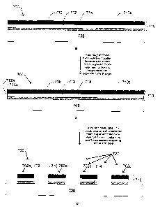
Figs. 7a-7c are schematic cross-sectional views of a process according to an
embodiment of the
present invention, including micro-roughening the surFace of a mixed-metal
layer, followed by etching of the
layer to form circuit pattern elements.
Fig. 8a-8c are schematic cross-sectional views of a process according to an
embodiment of the
present invention, including micro-roughening the surface of a single metal
layer, followed by etching of the
layer to form circuit pattern elements.
It should be appreciated that for simplicity and clarity of illustration,
elements shown in the Figures
have not necessarily been drawn to scale. For example, in some Figures, the
vertical dimensions of some
of the elements may be exaggerated relative to horizontal dimensions for
clarity. Further, where considered
appropriate, reference numerals have been repeated among, or corresponding
numbers have been used in,
the Figures to indicate corresponding elements.
DETAILED DESCRIPTION
It should be appreciated that the process steps and structures described below
do not form a
complete process flow for manufacturing and using a printed circuit board or
other end-product made by a
process including the present invention. The present invention can be
practiced in conjunction with
fabrication techniques currently used in the art, and only so much of the
commonly practiced process steps
are included as are necessary for an understanding of the present invention.
_g_
CA 02536836 2006-02-23
WO 2005/034596 PCT/US2004/031697
As used herein, the term "micro-roughening" may also be referred to as an
intergranular etching
process. The details of suitable micro-roughening methods and compositions are
described below. In the
micro-roughening process, the surface of a metal such as copper or a mixed-
metal is chemically treated to
increase both its surface area and its roughness. In one embodiment, in the
micro-roughening, the surface
is treated to increase its surface area by a factor of greater than 40%. In
another embodiment, in the micro-
roughening, the surface is treated to increase its surface area by a factor of
from about 40% to about 200%,
in one embodiment, in the micro-roughening, the surface is treated to increase
its surface area by a factor
of from about 50% to about 100% and in another embodiment, in the micro-
roughening, the surface is treated
to increase its surface area by a factor of from about 60% to about 120%.
Surface area may be measured
by any appropriate method. One suitable method for measuring surface area is
by use of a 3-D atomic force
microscope (AFM) topographic analysis of the surface. Suitable AFM apparatus
is commercially available,
for example, from Veeco Instruments Inc., Woodbury, NY.
In one embodiment, in the micro-roughening, the surface is treated to increase
its roughness to a
roughness (ra) as measured by profilometer in the range from about 0.2 micron
to about 0.6 micron, and in
another embodiment, in the micro-roughening, the surface is treated to
increase its roughness (ra) as
measured by profilometer in the range from about 0.3 micron to about 0.5
micron, and in one embodiment,
about 0.4 micron. Here, as elsewhere in the specification and claims, the
numerical limits of the disclosed
ranges and ratios may be combined. For example, the foregoing disclosure
includes a roughness (ra) as
measured by profilometer in a range of, e.g., about 0.2 micron to about 0.5
micron, and from about 0.3
micron to about 0.6 micron, although such were not explicitly set forth above.
Micro-roughening may be carried out by any of the methods described in detail
hereinbelow, or by
other suitable methods which may be known in the art.
Figs. 5 and 6 are photomicrographs of metal surfaces obtained from originally
identical metal
surfaces, which have been subjected, respectively, to micro-roughening and to
micro-etching. Thus, Fig. 5
is a photomicrograph of a metal surface which has been treated to increase its
surface area and roughness
by micro-roughening in accordance with the present invention. In the metal
layer shown in Fig. 5, the surface
area was increased by 107%, and the roughness (ra) as measured by profilometer
is 0.412 micron, as a
result of the micro-roughening. As shown in Fig. 5, the surface not only has
increased roughness (ra) as
measured by profilometer, but includes a significantly increased surface area.
As used herein, the term "micro-etching" refers to surface preparation in
which the surface of a metal
such as copper is chemically treated to form a matte surface having a
roughness (ra) as measured by
profilometer in the range from about 0.1 micron to about 0.3 micron, but which
generally does not include a
greatly increased surface area. Thus, micro-etching, as used herein, increases
the roughness of the surface
as measured by profilometer, and increases the surface area to some degree,
but less than the surface area
increase obtained by micro-roughening. The increase in surface area obtained
by micro-etching ranges from
about 5% to less than 40% at the greatest. Thus, while conventional micro-
etching processes increase the
roughness (ra) of the surface as measured by profilometer, such processes do
not obtain an increase in
surface area of the same magnitude as that which can be obtained by micro-
roughening. As known in the
art, the roughness (ra) as measured by profilometer is a measure of the peak-
to-valley height of surface
_g-
CA 02536836 2006-02-23
WO 2005/034596 . PCT/US2004/031697
features on the metal surface, and this measurement does not reflect changes
in surface area of the metal
surface.
Fig. 6 is a photomicrograph of a metal surface (obtained from the same
original metal surface as that
shown in Fig. 5), which has been treated by micro-etching. In the metal layer
shown in Fig. 6, the surface
area was increased by 21 %, and the roughness (ra) as measured by profilometer
is 0.252 micron, as a result
of the micro-etching. As shown in Fig. 6, the surface has an increased degree
of roughness (ra) as measured
by a profilometer, but does not exhibit the high surface area of the micro-
roughened metal surface shown
in Fig. 5, as described above. Thus, while the micro-etched metal surface has
a roughness (ra) as measured
by a profilometer in a range which may overlap the roughness (ra) as measured
by a profilometer of a micro-
roughened metal surface, the micro-etched metal surface has a much lower
surface area. This difference
is readily apparent by comparison of the metal surfaces depicted in Figs. 5
and 6.
Micro-etching may be carried out, for example, by applying a composition
including a persulfate or
a monopersulfate, such a OXONE~, which contains persulfate and is available
from E. I. Du Pont de
Nemours and Co., Inc.
As used herein, the term "pre-treatment roughening" refers to surface
preparation in which the
surface of a metal such as copper is treated to form, e.g, dendritic
structures on its surface, having a
roughness (ra) as measured by profilometer is in the range' from about 1
micron to about 3 microns.
Application of a dendritic surface to copper foil is described, for example,
in U.S. Patent No. 6,042,711,
assigned to Gould Electronics, Inc. Such pre-treatment roughening processes
are metal-deposition
processes as opposed to micro-etching and micro-roughening processes, which
are metal-removal
processes.
In the first embodiment, the invention relates to a process to improve
adhesion of dielectric materials
to a metal layer, including providing an unpatterned metal layer having a
first major surface; micro-roughening
the first major surface to form a micro-roughened surface; and etching the
metal layer to form a circuit pattern
in the metal layer, in which the micro-roughening is carried out prior to the
etching. In one embodiment, prior
to the micro-roughening, no surface treatment to increase the roughness of the
metal layer is carried out.
In one embodiment, no further surface treatment to increase the roughness of
the metal is carried out
subsequent to the etching to form the circuit pattern.
In the second embodiment, the invention relates to a process to improve
adhesion of dielectric
materials to a metal layer, comprising:
a. providing an unpatterned metal layer having a first major surface;
b. micro-roughening the unpatterned metal layer with a solution to form a
micro-roughened
surface on the first major surface;
c. applying an etch resist to the micro-roughened surface;
d. patterning the etch resist to reveal areas of metal to be removed;
e. etching the metal layer which is not protected by the etch resist to form a
circuit pattern;
f. removing the etch resist.
-10-
CA 02536836 2006-02-23
WO 2005/034596 PCT/US2004/031697
As in the first embodiment, in one embodiment of this second embodiment, no
further surface treatment to
increase the roughness of the metal is carried out subsequent to the etching
(e). In one embodiment, prior
to the micro-roughening, no surface treatment to increase the roughness of the
metal layer is carried out.
The micro-roughening and etching processes are described in detail in the
following. The process
description is provided for both copper-Invar-copper ("CIC") as the conductive
circuit material, and thereafter,
for copper as the conductive circuit material. The present invention is
applicable to copper and alloys of
copper with other metals, other metals and alloys including, for example,
aluminum, molybdenum, iron,
nickel, tin, zinc, beryllium, silicon, cobalt, phosphorus, lead, manganese,
magnesium and chromium, and to
other mixed-metal sandwiches, in addition to CIC, in which an inner layer of
another metal, such as, for
example, molybdenum or aluminum, is sandwiched between two out layers of
copper or copper alloy.
Although the currently most widely used mixed-metal sandwich is CIC, this
invention is broadly applicable
to any similar mixed-metal sandwich, in which an inner layer of one metal or
alloy is sandwiched between two
outer layers of other metals) or alloy(s), and at least one of the metal or
alloy of the inner layer interferes
electrolyticallywith surface etching of the outer metal layer(s). Unless
otherwise specified, the disclosure fully
applies to copper, copper alloys and to mixed-metal sandwiches. The effects
described herein are
particularly applicable to mixed-metal sandwiches in which the inner layer is
a metal which is more active
galvanically than the outer layers. However, as will be understood, a similar
effect may occur when the inner
layer is the less active metal. The processes described herein are fully
applicable to single layers, such as
copper or copper alloys, which are not susceptible to the same problems as are
mixed-metal layers. In such
single-layer cases, the benefits of the present invention include the
avoidance of loss of cross-sectional area
of formed circuit pattern elements, as described above with respect to Figs.
3a-3c_ Although specific
examples of products are given, they are not intended to limit the application
of the invention to the use of
those products.
MIXED-METAL LAYER
A process in accordance with the second embodiment of the present invention is
described with
reference to Figs. 7a-7c. Figs. 7a-7c are schematic cross-sectional views of a
process according to an
embodiment ofthe present invention, including micro-roughening the surface of
a mixed-metal layer, followed
by etching of the layer to form circuit pattern elements.
As a first step (a) in the second embodiment of the process of the present
invention, an unpatterned
metal or mixed-metal layer, such as an 18-20 inch wide sheet of copper or CIC,
is provided.
Fig. 7a is a schematic cross-sectional view of a nascent circuit 700, such as
a printed circuit board,
including an unpatterned mixed-metal layer 718 adhered or attached to a
dielectric material layer 708. The
mixed-metal layer 718 includes a top layer 710 of a first metal or alloy and
an inner layer 712 of a second
metal or alloy, and an underlying layer 714, which may be the same metal or
alloy as the top layer 710,
although in one embodiment, the underlying layer 714 may comprise a different
metal or alloy. The three
layers 710, 712 and 714 form the mixed-metal layer 718. The top layer 710 has
a first major surface 710a,
which in this embodiment is the only exposed surface of the mixed-metal layer
716, except for the side or
edge surfaces of the mixed-metal layer 718.
-11-
CA 02536836 2006-02-23
WO 2005/034596 PCT/US2004/031697
In one embodiment, the unpatterned mixed-metal layer 718 is provided in a
continuous roll, and in
another embodiment, the metal layer is provided in a square or rectangular
sheet. In one embodiment, the
unpatterned metal layer 718 is provided already adhered to a dielectric
material layer 708. In another
embodiment, the unpatterned mixed-metal layer 718 is provided and is
subsequently applied to the dielectric
material layer 708 prior to the micro-roughening and patterning. In yet
another embodiment, the unpatterned
mixed-metal layer 718 is provided, the micro-roughening carried out and the
circuit pattern formed, and
subsequently the formed circuit pattern is applied to the dielectric material
layer 708. In one embodiment,
prior to the micro-roughening, no surface treatment to increase the roughness
of the metal is carried out.
The CIC foils used with this invention are commercially available from, e.g.,
Texas Instruments, Inc.
and Gould Electronics, Inc., and are supplied as a clad starting material in
various inlay ratios. The inlay
ratios for the CIC may range, for example, from about 12.5%/75%/12.5% to about
30%/40%/30%, including,
for example 20%/60%/20%. CIC and similar mixed-metal layers may be provided in
a thickness of
approximately 6 mil (about 0.15 mm), for example. The CIC and similar mixed-
metal layers may be rolled
to reduce the thickness as appropriate, if needed.
Such metal foils may be provided in various panel sizes, such as 18" x 24",
12" x 18" or 20" by 24.5"
to about 26". Each panel generally comprises a plurality of sections, each of
which will eventually become,
for example, a single conductive layer of a PCB.
The metal layer may comprise any of the metals disclosed above, either as a
single layer or as a
mixed-metal sandwich. The metal layer has a first major surface, which is the
surface of the metal layer to
which the treatments disclosed herein are applied, and to which the dielectric
material will eventually be
applied. A second major surface of the metal layer may have been attached or
adhered, as by lamination,
to a dielectric material, in which case only the first major face is treated
as disclosed herein. In one
embodiment, the metal layer is not attached or adhered to a dielectric
material, in which case the second
major surface of the metal layer may also be treated as disclosed herein.
As known in the art, metal surfaces may be first cleaned to ensure that any
contamination on the
copper surface does not interfere with the copper surface treatment. Thus, in
one embodiment, the
unpatterned metal layer is cleaned prior to any further treatments being
applied. Any conventional cleaning
solution can be used. In one embodiment, surfactants and in other embodiments,
complexing agents (such
as triethanolamine), or in other embodiments, both surfactants and complexing
agents, are added to aqueous
cleaning solutions for improved cleaning ability. In many embodiments, an
aqueous alkaline cleaner is used
for removing residues, such as oils, dusts, etc., created by human contact
with the copper surface. In one
embodiment, the cleaning operation comprises application of a 100 ml/I
solution of Basiclean~ UC, supplied
by Atotech, in water. The solution may be sprayed onto the metal at about 20
psi at about 50°C for about
1 minute, for example, followed by rinsing with, e.g., deionized water.
Basiclean~ UC is an alkaline cleaner
including about 35 wt% sodium hydroxide.
Depending on the micro-roughening chemistry and the mode of application, it
may be helpful to
employ a pre-conditioning step to assist in making the micro-roughening
uniform over the entire surface of
the copper. By creating a uniform surface potential on the copper, the pre-
conditioner assists in initiating the
micro-roughening reaction at substantially the same time over the entire
surface area of the metal layer. The
-12-
CA 02536836 2006-02-23
WO 2005/034596 PCT/US2004/031697
pre-conditioner may comprise surfactants and/or components of the micro-
roughening composition, such
as alcohols, alkoxyalcohols, polyalkoxyalcohols, triazoles and other
components wt-~ich interact with the
surface of the metal layer.
In one embodiment, the pre-conditioner includes a water soluble alcohol. As
used herein, an alcohol
is water soluble when it has water solubility of at least about 0.05 M. In one
embodiment, the water soluble
alcohol may include one or more of C~-C6 straight chain and C3-Cg branched
chain alcohols, C2-C~2
alkoxyalcohols and C3-C24 polyalkoxyalcohols. In one embodiment, for example,
the alcohol may comprise
isopropyl alcohol, isopropoxyethanol, or ethoxyethoxyethanol. In another
embodiment, the pre-conditioner
includes a non-ionic surfactant such as a polyethoxyethanol. The number of
carbon atoms in the water
soluble alcohol may vary over a wide range, provided that the water soluble
alcohol retains water solubility,
as defined.
In another embodiment, the pre-conditioning solution may further include a
corrosion inhibitor.
Suitable corrosion inhibitors include, for example, triazoles such as
benzotriazole, tetrazole and substituted
tetrazoles, thiadiazoles, thiatriazoles, imidazoles, benzimidazoles, etc.
Suitable corrosion inhibitors are
known in the art, and are disclosed, for example, in U.S. Patent No. 6,506,314
B1, the disclosure of which
is incorporated by reference with respect to organic corrosion inhibitors.
A suitable pre-conditioning solution is commercially available from Atotech as
BondFilm~ Activator,
available from Atotech. In one embodiment, the pre-conditioner comprises a 20
mill solution of BondFilm~
Activator. BondFilm~ Activator contains isopropoxyethanol, benzotriazole and
other proprietary ingredients.
The metal is immersed in this solution for 30 seconds at 35°C. No
rinsing is needed or required between the
pre-conditioning step and the microroughening step because, as noted, the
additives in the pre-conditioner
interact with the metal surface to improve the micro-roughening reaction.
Following treatment with such pre-conditioning solution, it is generally not
necessary to rinse the
metal surface prior to the next step. In one embodiment, when the pre-
conditioning solution contains a
corrosion inhibitor which is the same or similar to that used in the following
micro-roughening treatment, it
is not necessary to rinse the pre-conditioned metal surface. In particular,
when the BondFilm~ Activator is
used for pre-conditioning, and the micro-roughening is carried out using
BondFilm~ from Atotech, not only
is rinsing not necessary, it is not desirable. This is because the pre-
conditioning treatment helps to prepare
the metal surface for the subsequent micro-roughening treatment, and thus the
treatm ent is desirable to be
retained on the surface.
In the next step (b) of the second embodiment of the process of the present
invention, shown in Fig.
7b, the first major surface 710a of the unpatterned mixed-metal layer 718 is
treated with a micro-roughening
solution, in a step of micro-roughening the surface 710a, to create a micro-
roughened surface 710b of the
unpatterned mixed-metal layer 718. A number of solutions suitable for micro-
roughen ing the surface 710a
in order to create the micro-roughened surface 710b are described in detail
hereinbelow.
As shown in Fig. 7b, following the micro-roughening, the unpatterned mixed-
metal layer 718 has a
micro-roughened surface 710b. In addition, as shown in Fig. 7b, the mixed-
metal layer 718 also includes an
un-etched edge portion 710c. As described above, this un-etched edge portion
710c is a portion of the top
layer 710 which remains un-etched as a result of the galvanic edge effect. As
schematically shown in Fig.
-13-
CA 02536836 2006-02-23
WO 2005/034596 PCT/US2004/031697
7b, in accordance with the present invention, the un-etched edge portion 71 Oc
advantageously occurs only
at the edges of the mixed-metal layer 718, leaving the entire remaining first
major face of the mixed-metal
layer 718 relatively evenly micro-roughened as desired. In the normal course
of preparing circuits such as
described herein, these edge portions 710c of the mixed-metal layer 718 would
be removed subsequent to
the pattern formation in any case. Since this area of the panel normally does
not contain active circuitry, the
lack of micro-roughening in this area does not reduce the quality or
performance of the final product. This
area is usually trimmed off when the individual circuits are removed from the
panel. Thus, the fact that these
edge portions 710c remain un-etched is not detrimental and creates no problem.
In fact, this overcomes the
problem of the edge effects which result from the un-etched portions of each
individual circuit element in the
conventional process, where the circuit pattern is first formed, and then is
micro-roughened to create the
improved adhesion to subsequently applied dielectric materials. In addition,
this addresses and substantially
avoids the problem of the reduction in size of each individual circuit element
resulting from post-circuit
element formation micro-roughening, which reduces the overall size of each
circuit element below its initially-
formed size.
As shown in Fig. 7b, the micro-roughening treatment forms a micro-roughened
edge portion 712a
of the inner layer 712.
As also shown in Fig. 7b, the edge of the underlying layer 714 is not etched
or roughened by the
micro-roughening treatment due to the galvanic edge effect described above. As
with the edge portion 71 Oc,
the lack of micro-roughening at this point does not adversely impact the
product, since this edge portion will
be removed subsequently.
In the next step (c), of the process of the present invention, an etch resist
is applied to the micro-
roughened surface. After the micro-roughened panels are rinsed and dried, a
suitable etch resist is applied
to the surface, according to conventional processes. This resist may be in the
form of a dry film, or it may
be a liquid. In either case, the micro-roughened surface improves the adhesion
of the etch resist such that
it will not delaminate during the developing or etching steps. Any known type
of etch resist and method of
application may be used with this process. In one embodiment, the etch resist
application operation
comprises contacting the metal surface with a film of DuPont PM 120 etch
resist and applying heat and
pressure to the film by passing the assembly through a pair of pinch rollers
which are heated to 110°C. In
one embodiment, the linear speed of travel through the pinch rollers is 1
meter/minute.
In the next step (d), of the process, the etch resist is patterned to reveal
areas of metal to be
removed in forming the circuit pattern. Etch resist patterning may be
performed by known processes,
including exposing the resist material to ultraviolet light or laser energy.
The exposure step may incorporate
a mask to prevent exposure of certain areas to create a desired pattern, or
the resist may be exposed by a
direct write method. In either case, the etch resist is then brought into
contact with a developing solution
which dissolves the less chemically-resistant areas of the resist to reveal
the underlying copper. Some etch
resists are then cured by heat or UV energy to make them less susceptible to
attack by the copper etching
solution. Using the aforementioned DuPont PM120 etch resist, in one
embodiment, a patterning operation
includes exposing the etch resist material to 40 mJ/cm2 of UV energy at a
wavelength of about 330 to about
400 nm through a polyester phototool. After exposure, the protective polyester
cover sheet is removed from
-14-
CA 02536836 2006-02-23
WO 2005/034596 PCT/US2004/031697
the etch resist. The etch resist is then brought into contact with a
developing solution containing 10 g/I
potassium carbonate at 30°C which is sprayed at 20 psi for 50 seconds.
In the next step (e), of the process, the metal layer which is not protected
is etched to form a circuit
pattern. After rinsing, the exposed metal areas of the surface 710b are etched
using oxidizing solutions
known in the art. For copper, in one exemplary embodiment, an acidic solution
based on cupric chloride and
hydrochloric acid may be used. Such a solution contains a free hydrochloric
acid concentration of 1.5N and
a specific gravity of 1.28 g/ml. At a temperature of 55°C and a spray
pressure of 20 psi, the copper etch rate
is approximately 28 micron/minute. For CIC, in one exemplary embodiment, an
etching solution comprises
ferric chloride and hydrochloric acid. Such a solution contains a free
hydrochloric acid concentration of 1.5N
and a specific gravity of 1.33 g/ml. At a temperature of 50°C and a
spray pressure of 20 psi, the Invar etch
rate is approximately 15 micron/minute and the copper etch rate is
approximately 30 micron/minute.
In the next step (f) of the process, the etch resist is removed. After etching
and rinsing the copper
or CIC, the etch resist is stripped with an appropriate stripping method. Any
stripping method compatible with
the etch resist that does not etch the metal can be used. For the
aforementioned DuPont PM120, in one
exemplary embodiment, the stripping operation includes contacting the etch
resist with an aqueous solution
containing 60 ml/I ResistStrip~ RR-3 supplied byAtotech. The solution is
sprayed onto the etch resist at a
temperature of 55°C for at least 60 seconds at a pressure of 30 psi.
Steps (c) through (f) are conventional, and are not shown in the drawings for
the sake of brevity.
Fig. 7c is a schematic cross-sectional view of a patterned micro-roughened
mixed-metal layer 716,
following the etching of the unpatterned mixed-metal layer 718 to form a
circuit pattern 720 comprising a
plurality of circuit pattern elements 702a-702d. As shown in Fig. 7c, the edge
portions 710c of the patterned
mixed-metal layer 716 (which were not micro-roughened due to the galvanic edge
effect; see Fig. 7b) have
been removed by the etching process in the embodiment shown in Fig. 7c. In
other embodiments, the edge
portions may be left in place, for example, to facilitate handling of the
etched metal layers, and subsequently
cut off during subsequent cutting or finishing operations. The removal or non-
removal of these edge portions
710c can be selected by adjusting the location of the etch resist layer.
As shown in Fig. 7c, following etching to form the circuit pattern 720, each
of the individual circuit
elements 702a-702d are formed with an initial, selected width, and with an
upper surface which has already
been micro-roughened. There is no subsequent micro-roughening carried out, so
each of the individual
circuit elements 702a-702d thereafter retain their initial, selected width and
none are left with upper surface
areas which have not been micro-roughened. It is not necessary to design and
etch the individual circuit
elements 702a-702d to have a larger initial size in order to compensate for a
size reduction which would
occur if the micro-roughening was carried out after the etching to form the
circuit pattern 720, and it is not
necessary to find a remedy to the problem of un-roughened edge portions
resulting from the galvanic edge
effect. This feature of the present invention allows the circuit designer to
design and build a mixed-metal
circuit pattern, with improved adhesion to subsequently applied dielectric
materials than would have been
possible with prior art methods.
-15-
CA 02536836 2006-02-23
WO 2005/034596 PCT/US2004/031697
COPPER AND OTHER NON-MIXED-METAL LAYERS
In another embodiment, a circuit board may include a single metal layer, such
as a layer of copper
or copper alloy.
Fig. 8a is a schematic cross-sectional view of a nascent circuit 800, such as
a printed circuit board,
including an unpatterned metal layer 810 adhered or attached to a dielectric
material layer 808. The metal
layer 810 includes a first major surface 810a which in this embodiment is the
only exposed major surface of
the metal layer 810.
In one embodiment, the unpatterned metal layer 810 is provided in a continuous
roll, and in another
embodiment, the metal layer is provided in a square or rectangular sheet. In
one embodiment, the
unpatterned metal layer 810 is provided already adhered to a dielectric
material layer 808. In another
embodiment, the unpatterned metal layer 810 is provided and is subsequently
applied to the dielectric
material layer 808 prior to the micro-roughening and patterning. In yet
another embodiment, the unpatterned
metal layer 810 is provided, the micro-roughening carried out and the circuit
pattern formed, and
subsequently the formed circuit pattern is applied to the dielectric material
layer 808.
The copper foils used with this invention are made using one of two
techniques. Wrought or rolled
copper foil is produced by mechanically reducing the thickness of a copper or
copper alloy strip or ingot by
a process such as rolling. Electrodeposited copper foil is produced by
electrolytically depositing copper ions
on a rotating cathode drum and then peeling the deposited foil from the
cathode. Electrodeposited copper
or copper-alloy foils are especially useful with this invention. Foils of
metals other than copper may be
produced by similar, known processes.
When the metal layers are metal foils, they typically have nominal thicknesses
ranging from about
2.5 pm to about 500 pm or more. Foil thickness, and particularly copper foil
thickness, may be expressed
in terms of weight and typically the foils of the present invention have
weights or thicknesses ranging from
about 0.35 to about 43 gldm2 (about 1/8 to about 14 ounces per square foot
(oz/ft2)). Especially useful
copper foils are those having weights of %2, 1 or 2 ozlft2 (1.52, 3.05 or 6.10
g/dm2).
In the next step (b) of the second embodiment of the process of the present
invention, shown in Fig.
8b, the first major surface 810a of the unpatterned metal layer 810 is treated
with a micro-roughening
solution, in a step of micro-roughening the surface 810a, to create a micro-
roughened major surface 810b,
and a micro-roughened side surface 81 Oc, of the unpatterned metal layer 810
as shown in Fig. 8b. A number
of solutions suitable for micro-roughening the surface 81 Oa may be employed
to create the micro-roughened
surfaces 810b and 810c, and several are disclosed below. In one embodiment,
the micro-roughening may
also be referred to as intergranular etching.
As shown in Fig. 8b, following the micro-roughening, the unpatterned metal
layer 810 has the micro-
roughened surface 810b. In this embodiment, as shown in Fig. 8b, the metal
layer 810 also includes an
etched edge portions 810c. In contradistinction to the mixed-metal embodiment
described above, the edge
portion 810c is etched in this embodiment since there is no effect from an
inner layer made of a different
metal and causing a galvanic edge effect. As schematically shown in Fig. 8b,
the entirety of the exposed
surfaces of the metal layer 810 are relatively evenly micro-roughened as
desired. As will be described in
more detail below, micro-roughening at this point results in avoidance or
significant or nearly complete
-16-
CA 02536836 2006-02-23
WO 2005/034596 PCT/US2004/031697
reduction of the problem of the reduction in cross-sectional area of each
individual circuit element and
concomitant increase in resistivity, as described above with respect to Figs.
3a-3c.
In the next step (c) of this embodiment of the process of the present
invention, an etch resist is
applied to the micro-roughened surface. After the micro-roughened panels are
rinsed and dried, a suitable
etch resist is applied to the micro-roughened surface 810b, according to
conventional processes. This resist
may be in the form of a dry film, or it may be a liquid. In either case, the
micro-roughened surface 810b
improves the adhesion of the etch resist such that it will not delaminate
during the developing or etching
steps. Any known type of etch resist and method of application may be used
with this process. In one
embodiment, the etch resist application operation comprises contacting the
metal surface with a film of
DuPont PM 120 etch resist and applying heat and pressure to the film by
passing the assembly through a
pair of pinch rollers which are heated to 110°C. The linear speed of
travel through the pinch rollers is 1
meterlminute.
In the next step (d) of the process, the etch resist is patterned to reveal
areas of metal to be removed
in forming the circuit pattern, as described above with respect to the CIC
embodiment described with respect
to Fig. 7a-7c. That disclosure is not repeated here for the sake of brevity,
but is incorporated by reference
with respect to this embodiment.
In the next step (e) of the process, the metal layer which is not protected is
etched to form a circuit
pattern. After rinsing, the exposed metal areas are etched using oxidizing
solutions known in the art, as
described above with respect to the CIC embodiment described with respect to
Fig. 7a-7c. That disclosure
is not repeated here for the sake of brevity, but is incorporated by reference
with respect to this embodiment.
In the next step (f) of the process, the etch resist is removed. After etching
and rinsing the copper,
the etch resist is stripped with an appropriate stripping method, as described
above with respect to the CIC
embodiment described with respect to Fig. 7a-7c. That disclosure is not
repeated here forthe sake of brevity,
but is incorporated by reference with respect to this embodiment.
Steps (c) through (f) are conventional, and are not shown in the drawings for
the sake of brevity.
Fig. 8c is a schematic cross-sectional view of a micro-roughened mixed-metal
layer 816, following
the etching of the layer 816 to form a circuit pattern 820 comprising a
plurality of circuit pattern elements
802a-802d, and subsequent removal of the etch resist. As shown in Fig. 8c, the
edge portions 810c of the
metal layer 810 (see Fig. 8b) have been removed by the etching process in the
embodiment shown in Fig.
8c. In other embodiments, the edge portions may be left in place, for example,
to facilitate handling of the
etched metal layers, and subsequently cut off during finishing operations. The
removal or non-removal of
these edge portions 810c can be selected depending on the location of the etch
resist layer.
As shown in Fig. 8c, following etching to form the circuit pattern 820, each
of the individual circuit
elements 802a-802d are formed with an initial, selected width, and with an
upper surface which has already
been micro-roughened. In one embodiment, there is no subsequent micro-
roughening carried out, so each
of the individual circuit elements 802a-802d thereafter retain their initial,
selected width. Thus, it is not
necessary to design and etch the individual circuit elements 802a-802d to have
a larger size to compensate
for a size reduction which would occur if the micro-roughening was carried out
after the etching to form the
circuit pattern 820. This feature of the present invention allows the circuit
designer to design and build a
-17-
CA 02536836 2006-02-23
WO 2005/034596 PCT/US2004/031697
smaller circuit pattern, with more narrowly spaced individual circuit pattern
elements, than would be possible
with prior art methods, in which the circuit pattern would have to be made
larger initially.
At this point, in one embodiment, the process according to the present
invention is complete. The
etched metal layer having the circuit pattern may thereafter be treated
according to known processes, for
example, in applying chemical surface treatments or coatings for, e.g.,
enhancement of adhesion to dielectric
materials, prevention of corrosion, etc., and in applying a dielectric
material. Some suitable exemplary
treatments are described in the following.
In the third embodiment of the present invention, additional steps are
included, specifically, a
dielectric material layer is applied, and optionally, a metal layer may be
applied to further enhance adhesion
to the dielectric material.
The steps (a)-(f) of the third embodiment may be substantially the same as
those described above
with respect to the second embodiment.
In the next step (h) of the third embodiment of the process of the present
invention, a dielectric
material layer is applied to the micro-roughened surface of the circuit
pattern. After rinsing and drying, the
patterned circuit is ready for dielectric application. The surface is already
appropriately micro-roughened to
have reliable adhesion to dielectric material. However, certain dielectric
materials which exhibit poor
adhesion to copper may show improved adhesion when a secondary metal is
applied by chemical reaction
to the surface of the micro-roughened copper. For example, a thin layer of tin
may be applied to the copper
surface using a replacement reaction, also known as an immersion tin process.
Other metals which can
enhance adhesion to dielectric materials include, but are not limited to,
nickel, bismuth, lead, zinc, indium,
palladium, ruthenium, chromium, and cobalt, as well as oxides and alloys of
these materials where the
specified metal is at least 50 percent by weight of the alloy. An example of
such an alloy is
nickel-phosphorous, where the phosphorous content of the alloy is 6% to 15% by
weight. In one
embodiment, the secondary metal layer is very thin, so that the surface
structure of the underlying copper
is not substantially modified.
In an optional step (g) of either the second or third embodiments of the
process of the present
invention, a secondary metal coating may be applied to the micro-roughened
surface. In one embodiment,
a secondary metal application operation includes contacting the patterned
metal structures with a solution
of Securer"" Enhancer supplied by Atotech. The solution contains 500 ml/I
Securer"' Enhancer 300, 83 ml/I
Securer"' Enhancer 400, and 100 ml/I sulfuric acid (sp. gr. 1.8). In one
embodiment, at a temperature of
35°C, the immersion time is about 40 seconds. This will leave a tin
layer on the copper or CIC that is
approximately 0.15 microns thick, and the underlying copper structure is not
substantially modified. That is,
the micro-roughened surface is simply coated, and its overall shape is
retained. In other embodiments,
additional coatings known in the art may be applied to the secondary metal to
further enhance the dielectric
adhesion, such as organo-silane materials.
Prior to application of the dielectric layer, it is generally advantageous to
inspect the patterned micro-
roughened metal structures. This inspection usually includes an optical
observation of the patterned
structures, either manually by a human or automatically by a computerized
machine. In order to aid the
optical inspection operation, an additional step may be added prior to etch
resist application or after etch
-18-
CA 02536836 2006-02-23
WO 2005/034596 PCT/US2004/031697
resist stripping in order to chemically adjust the color of the micro-
roughened surface. In either case, the
color adjustment operation should not substantially modify the micro-roughened
surface structure. Color
adjustment can be performed by any chemical reaction. In one embodiment, the
color adjustment operation
includes contacting the micro-roughened metal with an aqueous solution
containing 10 ml/I sulfuric acid (s.
g. 1.8) and 10 ml/I of 35 wt% hydrogen peroxide. The solution is sprayed onto
the micro-roughened surface
at 20 psi for 20 seconds at 35°C. Subjecting a copper surface that was
micro-roughened with BondFilm~
to such a color adjustment operation changes the surface color from dark brown
to light orange-pink, and
the surface structure is not substantially modified.
The dielectric may be applied by any means used in the industry. Certain
dielectric materials are
available in liquid form and are cast onto the surface and cured. Other
dielectric materials are available in
a B-stage cured sheet and require heat and pressure to bond reliably to the
patterned metal structures. Still
other dielectric materials are applied by plasma vapor depos ition. The type
of dielectric used and the method
of application vary depending on the product. The invention can be used for
all of these applications.
MICRO-ROUGHENING PROCESSES
A number of suitable micro-roughening processes are known for use with the
present invention.
Several such processes are briefly described in the following disclosure.
These are meant to be exemplary
only, and the invention is not necessarily limited to any of them.
In one embodiment, the micro-roughening is carried by use of an aqueous
composition containing
an acid, an oxidizer and a corrosion inhibitor. In one embodiment, the
oxidizer may be, for example,
hydrogen peroxide at a concentration of about 6 to about 60 grams per liter
(g/I), or from about 12 g/I to about
g/I. In one embodiment, the oxidant includes one or more of a peroxide, a
peracid, a halide, a nitrate,
cupric ion, ferric ion or other metal ion capable of oxidizing the metal
surface. The acid may be any acid,
such as a mineral acid like sulfuric acid, in one embodiment, at a
concentration from about 5 g/I to about 360
g/I, or about 70 g/I to about 110 g/I of the composition. The corrosion
inhibitor may be one or more of
25 triazoles, benzotriazoles, tetrazoles, imidazoles, benzimidazoles and
mixtures of the foregoing. In one
embodiment, the corrosion inhibitor concentration may range from about 1 g/I
to about 20 g/I, or from about
6 g/I to about 12 g/I. In one embodiment, the composition may also include a
water soluble polymer such as
polyethylene glycol, polypropylene glycol, polyvinyl alcohol, and mixtures of
the foregoing.
In one embodiment, the micro-roughening composition is BondFilm~ supplied by
Atotech. The
30 BondFilm~ micro-roughening composition is provided as BondFilm~ Part A and
BondFilm~ Part B.
BondFilm~ includes hydrogen peroxide; sulfuric acid and benzotriazole,
together with other proprietary
ingredients.
Additional examples of such micro-roughening processes are described in U.S.
Patent Nos.
6,036,758, 0,294,220, 5,807,493 and 6,506,314, the disclosures of which are
hereby incorporated by
reference for their teachings with respect to such roughening processes (which
may be referred to by terms
other than "micro-roughening". For example, in U.S. Patent No. 6,506,314,
micro-roughening is referred to
as intergranular etching. This patent describes a number of suitable micro-
roughening compositions, any
one of which may be used in carrying out the present invention. The following
micro-roughening
compositions are disclosed in U.S. Patent No. 6,506,314, and are briefly
reviewed herein.
-19-
CA 02536836 2006-02-23
WO 2005/034596 PCT/US2004/031697
In one embodiment, the micro-roughening is carried out by applying an aqueous
composition
comprising (a) hydrogen peroxide; (b) at least one acid; (c) at least one
nitrogen-containing, five-membered
heterocyclic compound which does not contain any sulphur, selenium or
tellurium atom in the heterocycle;
and (d) at least one adhesive compound from the group consisting of sulfinic
acids, seleninic acids, tellurinic
acids, heterocyclic compounds containing at least one sulphur, selenium and/or
tellurium atom in the
heterocycle, and sulfonium, selenonium and telluronium salts having the
general formula (I),
R~
A+ X- (I)
/ \
R3 R2
wherein in formula (I)
A is S, Se or Te;
R~, R~ and R3 are independently C~-C6 alkyl, substituted alkyl, alkenyl,
phenyl, substituted phenyl, benzyl,
cycloalkyl, substituted cycloalkyl, R~, R2 and R3 being the same or different;
and
X- is an anion of an inorganic or organic acid or hydroxide, provided that the
acid selected to constitute
component (b) is not identical to the sulfinic, seleninic or tellurinic acids
selected as component (d).
In one embodiment of the micro-roughening composition, component (c) comprises
one or more
nitrogen containing heterocyclic compounds selected from triazoles,
tetrazoles, imidazoles, pyrazoles and
purines.
In one embodiment of the micro-roughening composition, component (c) is a
triazole of the chemical
formula (II):
(11)
N\ R~s
N
H
wherein in formula (II), R~~ and R~a may be hydrogen, alkyl, substituted
alkyl, phenyl, substituted phenyl,
amino, carboxyalkyl, and whereby R~~ and Rig may be the same or different, or
in which R~~ and R~$ may
be combined to form homo- or heterocyclic rings condensed with the triazole
ring.
In one embodiment of the micro-roughening composition, component (c) is a
tetrazole of the
chemical formula (III):
N
N (III)
\N ~R~s
H
-20-
CA 02536836 2006-02-23
WO 2005/034596 PCT/US2004/031697
wherein in formula (III), R~9 may be hydrogen, alkyl, substituted alkyl,
phenyl, substituted phenyl, haloalkyl,
amino, benzyl, carboxy, carboxyalkyl, alkoxycarbonyl, aminocarbonyl, R~2-CONH-
wherein R~2 may be as
defined above.
In one embodiment, the tetrazole is 5-aminotetrazole. In another embodiment,
the tetrazole is 5-
phenyltetrazole.
In one embodiment of the micro-roughening composition, component (c) includes
an imidazole
compound. In another embodiment, the imidazole is benzirnidazole.
Exemplaryembodiments of component (c) are 5-phenyltetrazole, benzotriazole,
methylbenzotriazole
and ethylbenzotriazole. In one embodiment, the microroughening composition of
this embodiment includes
a combination of a nitrogen-containing heterocyclic compound, such as
benzotriazole, methylbenzotriazole,
ethylbenzotriazole, 5-aminotetrazole or 5-phenyltetrazole, as component (c),
with heterocyclic compounds
such as aminothiophene carboxylic acids, their esters or amides,
aminothiazolenes and substituted
aminothiazofenes, as component (d).
In one embodiment of the micro-roughening composition, component (d) is a
sulfinic acid selected
from aromatic sulfinic acids and compounds having the general formula (IV):
RøR5N-C-SOZH (IV)
R6
wherein in formula (IV),
R4, R5 and R6 = H, alkyl, substituted alkyl, phenyl, substituted phenyl, R~-
(CO)-, wherein R7 = H, alkyl,
substituted alkyl, phenyl, substituted phenyl, and wherein R4, R5 and R6 may
be the same or different.
In one embodiment, component (d) is formamidine sulfinic acid.
In one embodiment of the micro-roughening composition, component (d) comprises
one or more
heterocyclic compounds selected from thiophenes, thiazoles, isothiazoles,
thiadiazoles and thiatriazoles. In
another embodiment, component (d) comprises one or more sulfinic acid
compounds selected from benzene
sulfinic acid, toluene sulfinic acid, chlorobenzene sulfinic acid,
nitrobenzene sulfinic acid and carboxybenzene
sulfinic acid. In another embodiment, component (d) comprises one or more
sulfonium salts selected from
trimethyl sulfonium salts, triphenyl sulfonium salts, methioninealkyl
sulfonium salts, and methionine
benzylsulfonium salts.
In one embodiment of the micro-roughening composition, component (d) is a
thiophene compound
having the chemical formula (V):
R9 Rio
Ra \ ~ R~ ~
S
-21-
CA 02536836 2006-02-23
WO 2005/034596 PCT/US2004/031697
wherein in formula (V),
R8, R9, R1° and R11 may be hydrogen, alkyl, substituted alkyl, phenyl,
substituted phenyl, halogen, amino,
alkylamino, dialkylamino, hydroxy, alkoxy, carboxy, carboxyalkyl,
alkoxycarbonyl, aminocarbonyl,
R12-CONH-, wherein R12 may be hydrogen, alkyl, substituted alkyl, phenyl,
substituted phenyl, whereby R8,
R9, R1° and R11 may be the same or different, or wherein two or more of
R8, R9, R1° and R11 may be
combined to form homo- or heterocyclic rings condensed with the thiophene
ring.
In one embodiment, the thiophene is an aminothiophenecarboxylic acid, ester or
amide. In another
embodiment, the thiophene is 3-aminothiophene-2-carboxylate methyl ester.
In one embodiment of the micro-roughening composition, component (d) is a
thiazole of the chemical
formula (VII):
R14
N
(VII)
R13 \S 'R15
wherein in formula (VII),
R13~ R1a and R15 may be hydrogen, alkyl, substituted alkyl, phenyl,
substituted phenyl, halogen, amino,
alkylamino, dialkylamino, hydroxy, alkoxy, carboxy, carboxyalkyl,
alkoxycarbonyl, aminocarbonyl,
R12-CONH-, wherein R12 may be as defined above, whereby R13, R1a and R15 may
be the same or different,
or in which two or more of R13, R1a and R15 may be combined to form homo- or
heterocyclic rings condensed
with the thiazole ring.
In one embodiment, the thiazole is an aminothiazole or a substituted
aminothiazole. In addition, the
compounds of component (d) may be thiadiazoles substituted with the same R
groups as above. In one
embodiment, the thiadiazole is an aminothiadiazole or a substituted
aminothiadiazole.
The components of this embodiment of the micro-roughening solution, when
present, may be
present in the following exemplary concentration ranges:
Sulfuric acid, concentrated: 10 to 250 g/I
Hydrogen peroxide, 30 wt% solution: 1 to 100 g/I
5-membered nitrogen-containing
heterocyclic compound: 0.5 to 50 g/I
Adhesive compounds containing
sulfinic, selenic or telluric acids: 0.05 to 10 g/I
Adhesive heterocyclic compounds: 0.05 to 20 g/I
Sulfonium, Selenonium or Telluronium salts 0.01 to 10 g/I
The foregoing micro-roughening solution may be suitably applied as further
described in U.S. Patent No.
6,506,314.
-22-
CA 02536836 2006-02-23
WO 2005/034596 PCT/US2004/031697
In one embodiment, the micro-roughening is carried out by applying an aqueous
composition
comprising from about 5 g/I to about 50 g/I hydrogen peroxide and about 0.1
g/I to about 50 g/I of an aromatic
sulfonic acid or a salt thereof, such as sodium m-nitrobenzene sulfonate or
other known aromatic sulfonic
acids such as benzene sulfonic acids, which may be unsubstituted or
substituted by one or more substituents,
such as nitro, hydroxy, halogen, lower (C~-C6) alkyl, lower (C~-C6) alkoxy and
other substituents. The sulfonic
acid may be present as a salt, such as alkali metal salts. In alternative
embodiments, the oxidizing agent rnay
be ferric nitrate, ferric sulfate, sodium persulfate, etc., although hydrogen
peroxide is more often used. In
one embodiment, the composition may further include an inorganic acid, such as
sulfuric acid. In one
embodiment of the above-described peroxide/sulfonic micro-roughening
composition, the composition
includes a corrosion inhibitor, such as benzotriazole, other triazoles,
tetrazoles and imidazoles.
In one embodiment, the micro-roughening is carried out by applying an aqueous
composition
comprising (a) a cupric ion source, (b) an organic acid with an acid
dissociation constant (pKa) of 5 or lower,
(c) a halide ion source, and (d) water. This micro-roughening process may use
as the cupric ion source one
or more compounds) selected from a cupric salt of an organic acid, cupric
chloride, cupric bromide and
cupric hydroxide. The organic acid having a pKa of 5 or lower may be one or a
mixture of organic acids, such
as formic acid, acetic acid, propionic acid, butyric acid, valeric acid,
caproic acid, acrylic acid, crotonic acid,
iso-crotonic acid, oxalic acid, malonic acid, succinic acid, glutaric acid,
adipic acid, pimelic acid, malefic acid,
benzoic acid, phthalic acid, cinnamic acid, glycolic acid, lactic acid, malic
acid, citric acid, sulfamic acid,
(3-chloropropionic acid, nicotinic acid, ascorbic acid, hydroxyl pivalic acid
and levulinic acid. The halide ion
may be provided in the form of a halide acid or a salt thereof.
In one embodiment, the micro-roughening is carried out with an aqueous
composition comprising
0.1 to 20% by weight hydrogen peroxide; an inorganic acid; an organic
corrosion inhibitor; and a surfactant.
The hydrogen peroxide may be present at a concentration, in one embodiment,
from about 0.01 % by weight
up to about 20% by weight of the composition, and in one embodiment, from
about 3% to about 10% by
weight. The inorganic acid may be, for example sulfuric acid or phosphoric
acid, and may be present at a
concentration, in one embodiment, from about 1 % by weight to about 50% by
weight, and in another
embodiment, about 10% by weight to about 30% by weight. The corrosion
inhibitor may be one or more
selected from triazoles, tetrazoles and imidazoles, and mixtures thereof, for
example benzotriazole, which
may be substituted with, for example, C~-C4 alkyl substituents. The corrosion
inhibitor may be present in the
composition, in one embodiment, from 0.0001 % by weight to about 1 % by weight
of the composition, and in
one embodiment, from about 0.1 % to about 0.5%. The surfactant may be a
cationic surfactant, such as an
amine surfactant, or a quaternary ammoniu m surfactant. The surfactant may be
present at a concentration,
in one embodiment, from about 0.001 % by weight to about 5% by weight of the
composition, and in one
embodiment, about 0.01 % to about 1 % by weight.
In one embodiment, the micro-roughening is carried out with an aqueous
composition comprising
(a) an acid; (b) a copper complexing agent; (c) a metal capable of having a
multiplicity of oxidation states
which is present in one of its higher positive oxidation states and which
metal forms a composition soluble
salt, and (d) oxygen. The acid may be a mineral acid, such as sulfuric or
fluoboric, or an organic acid, such
as acetic acid, an alkane sulfonic acid, an al kanol sulfonic acid, or
mixtures of any thereof. The acid may be
-23-
CA 02536836 2006-02-23
WO 2005/034596 PCT/US2004/031697
present at a concentration, in one embodiment, from about 20 to about 400
grams of acid, and in one
embodiment, from about 50 to about 150 grams of acid, per liter of the micro-
roughening composition. The
pH of the composition may range from zero to about 6, and in one embodiment,
from zero to about 3. The
complexing agent may be at least one selected from urea and thiourea
compounds, amidines, and imidazole
thiones, such as, for example, thiourea or 1-methyl-3-propyl imidazole-2-
thione. The complexing agent may
be present at a concentration, in one embodiment, ranging from about 5 to
about 200 g/I of composition, and
in one embodiment, from about 25 to about 75 g/I of composition. The metal is
one or more metals capable
of having a multiplicity of oxidation states, which metal is present in one of
its higher positive oxidation states,
and which metal forms a composition soluble salt. Examples of such metals
include tin, lead, platinum, and
palladium which have positive oxidation states of +2 and +4; bismuth and
antimony which have positive
oxidation states of +3 and +5; and cerium and titanium which have positive
oxidation states of +3 and +4.
The composition should contain more than 4 grams per liter of the metal in the
higher oxidation state. The
amount of oxygen present in the composition ranges from about 1 to about 15 mg
per liter of composition,
and in one embodiment, from about 5 to about 9 mg per liter of composition.
The metal ion acts as an
oxidizing agent for copper in the micro-roughening, and is reduced from the
higher positive oxidation state
to the lower positive oxidation state. The metal is then re-oxidized to its
higher oxidation state by the oxygen
in the composition. The composition also may include one or more surfactants
compatible with each of the
metal salts, the acids and the complexing agent. The surfactant may be in a
concentration, in one
embodiment, from about 0.01 to about 100 grams per liter of bath, or from
about 0.05 to about 20 grams per
liter of the composition.
The processing conditions of the various embodiments of the micro-roughening
may be suitably
selected to yield the optimum micro-roughened surface of the metal layer,
based on the particular metal
substrate, i.e., copper, a copper alloy, etc. In general, the micro-roughening
may be carried out at a process
temperature in the range from about 10°C to about 75°C, for a
period of from about 1 minute to about 100
minutes, at atmospheric pressure.
In general, the greater the surface roughness, the greater will be the
adhesion to dielectric material.
However, as in the case of pre-treated CIC foil, too much roughness creates
problems with etch resist
patterning and stripping. In one embodiment, the process for creating micro-
roughness includes use of
BondFilm~, supplied byAtotech. This solution consists of 250 ml/I BondFilm~
Part A and 35 ml/I BondFilm~
Part B. The metal is immersed in this solution for 60 seconds at 35°C.
Typically, the amount of copper
removed by this process is from about 1.0 to about 1.5 microns, and the
surface roughness (ra), as measured
by a profilometer, is for example, from about 0.2 to about 0.4 microns. By
comparison, pre-treated CIC foil
has surface roughness (ra), as measured by a profilometer, in the range from
about 1 to about 3 microns.
The resist lock-in issues common to pre-treated foils are not likely to occur
with micro-roughening processes
using BondFilm~ due to the lower surface roughness as compared to the pre-
treated, e.g., dendritic surface.
While the invention has been, explained in relation to certain specific
embodiments, it is to be
understood that various modifications thereof will become apparent to those
skilled in the art upon reading
the specification. Therefore, it is to be understood that the invention
disclosed herein is intended to cover
such modifications as fall within the scope of the appended claims.
-24-