Note : Les descriptions sont présentées dans la langue officielle dans laquelle elles ont été soumises.
CA 02540589 2006-03-29
WO 2005/031288 PCT/CA2004/001701
RADIATION SENSOR DEVICE AND RADIATION SOURCE
MODULE CONTAINING SAME
FIELD OF THE INVENTION
In one of its aspects, the present invention relates to a radiation source
assembly. In another of its aspects, the present invention relates to a
radiation source
module comprising a novel radiation source assembly having incorporated
therein an
optical radiation sensor.
DESCRIPTION OF THE PRIOR ART
Optical radiation sensors are known and find widespread use in a number
to of applications. One of the principal applications of optical radiation
sensors is in the
field of ultraviolet radiation fluid disinfection systems.
It is known that the irradiation of water with ultraviolet light will
disinfect
the water by inactivation of microorganisms in the water, provided the
irradiance and
exposure duration are above a minimum "dose" level (often measured in units of
microWatt seconds per square centimetre). Ultraviolet water disinfection units
such
as those commercially available from Trojan Technologies Inc. under the
tradenaanes
Trojan UV MaxTM, Trojan UV LogicTM and Trojan W SwiftTM, employ this principle
to disinfect water for human consumption. Generally, water to be disinfected
passes
through a pressurized stainless steel cylinder which is flooded with
ultraviolet
2o radiation. Large scale municipal waste water treatment equipment such as
that
commercially available from Trojan Technologies Inc. under the trade-names
UV3000TM, UV3000 PIusTM and UV4000TM, employ the same principle to disinfect
waste water. Generally, the practical applications of these treatment systems
relates
to submersion of a treatment module or system in an open channel wherein the
wastewater is exposed to radiation as it flows past the lamps. For further
discussion
of fluid disinfection systems employing ultraviolet radiation, see any one of
the
following:
United States patent 4,482,809,
United States patent 4,872,980,
3o United States patent 5,006,244,
1
CA 02540589 2006-03-29
WO 2005/031288 PCT/CA2004/001701
United States patent 5,418,370,
United States patent 5,539,210, and
United States patent Re36,896.
Most commercially available ultraviolet radiation fluid treatment systems
employ so-called low pressure (including low pressure/high output) lamps
(e.g., such
systems available from Trojan Technologies Inc. under the trade-names UV3000TM
and UV3000 PlusTM) or medium pressure lamps (e.g., such systems available from
Trojan Technologies Tiic. under the trade-name UV4000TM).
In many applications, it is desirable to monitor the level of ultraviolet
to radiation present within the water under treatment. In this way, it is
possible to
assess, on a continuous or semi-continuous basis, the level of ultraviolet
radiation, and
thus the overall effectiveness and efficiency of the disinfection process.
It is known in the art to monitor the ultraviolet radiation level by deploying
one or more passive sensor devices near the operating lamps in specific
locations and
orientations which are remote from the operating lamps. These passive sensor
devices may be photodiodes, photoresistors or other devices that respond to
the
impingement of the particular radiation wavelength or range of radiation
wavelengths
of interest by producing a repeatable signal level (in volts or amperes) on
output
leads.
2o Conventional passive sensor devices (e.g., photodiodes, photoresistors and
the like) used to monitor ultraviolet radiation levels are responsive to light
according
to the light absorbing properties of the active material in the sensor. For
example,
silicon-based detectors commonly used in light detection are responsive to
light over
the range of from about 125 nm to about 1100 nm. This range of sensitivity
encompasses many types of radiation and is much larger than needed to detect
radiation in the ultraviolet region - i.e., radiation having at least one
wavelength in the
range of less that about 300 nm, ideally from about 240 nm to about 290 nrn
for
disinfection andlor from about 175 to about 300 mn for treatment of chemical
contaminants. The term "treatment of contaminants" is intended to mean
reduction of
the concentration of one or more contaminants in the water - in some cases, it
can
result in complete removal of the contaminant.
2
CA 02540589 2006-03-29
WO 2005/031288 PCT/CA2004/001701
The use of such conventional passive sensor devices can result in
inaccurate irradiance values in a disinfection system if a broad range of
radiation is
present in the disinfection system - i.e., radiation falling broadly in the
range of from
about 290 nm to about 1100 nm. Conventional silicon-based sensors also suffer
from
degradation in performance when exposed to the high intensity ultraviolet
radiation
used for prolonged periods of time in fluid treatment and/or disinfection
systems.
A relatively recent development in the art of ultraviolet radiation fluid
treatment systems is the use of a silicon carbide (SiC) detector as a sensing
device.
The relatively large bandgap of SiC narrows the wavelength range over which
the
1o detector is sensitive - i.e., to a wavelength range of from about 220 nm to
about 400
nm. Thus, the SiC detector is relatively insensitive to radiation having at
least one
wavelength greater than about 400 nm. In turn, this can reduce the likelihood
that the
above-mentioned measurement error will occur. More information on this
application
of SiC detectors may be found in United States patent 6,057,917 [Petersen et
al.] and
United States patent application publication 2002/162,970 [Sasges].
A~i emerging application of fluid treatment systems which utilize medium
pressure mercury lamps is the removal of chemical contaminants and dissolved '
organic carbon in water. Ultraviolet radiation having a wavelength in the
range of
from about 175 mn to about 300 nm is suitable for this application, where the
exact
2o wavelength range depends on the specific application. Unfortunately,
silicon carbide
is only responsive to radiation having a wavelength of greater than about 220
nm and
thus a sensor device using SiC is not well suited for monitoring UV light
intensity in
the lower wavelength range for applications such as chemical contamination
removal.
United States patent 6,611,375 [Knapp] teaches selectively tuned
ultraviolet optical filters and methods of use thereof. More specifically,
Knapp
teaches optical filters that purportedly are tuned specifically for
ultraviolet water
purification, and, as such, these optical filters are said to be characterized
by: (i)
transmitting effectively within the wavelengths that contribute to ultraviolet
sterilization (centered at 254 nm); (ii) selectively rejecting those
background discrete
3o wavelengths in the UV/VIS/IR emission spectra of typical mercury lamps and
which
fall within the sensitivity region of photodiodes; and (iii) are resistant to
damage from
high intensity ultraviolet radiation. More, particularly, Knapp teaches
optical filters
3
CA 02540589 2006-03-29
WO 2005/031288 PCT/CA2004/001701
having: (i) an optical transmittance of at least about 40%, more preferably at
least
about 70%, still more preferably at least about 75% or 79% at a wavelength of
about
254 nm, and (ii) an optical transmittance of no greater than 5% at wavelengths
of 313
nm to 580 nm and 1000 nm to 1140 nm. The profile of a sensor device employing
such an optical filter is illustrated in Figure 11 of Knapp - this Figure
illustrates that
the optical filter of I~napp allows radiation having a wavelength in the range
of from
about 600 nm to about 950 nm to pass therethrough. Unfortunately, even
radiation
having a wavelength in the range of from about 600 nm to about 950 nm can
result in
inaccurate irradiance values for conventional silicon-based photodiodes - this
issue is
l0 not addressed or otherwise dealt with in the teachings of Knapp.
Thus, despite the advances made in the art, there is room for improvement.
Specifically, it would be desirable to have a radiation sensor device
(particularly for
use in ultraviolet radiation fluid treatment systems) capable of detecting and
responding to radiation having at least one wavelength in the range of from
about 175
nm to about 350 nm while avoiding the disadvantages of the prior art.
DISCLOSURE OF THE INVENTION
It is an object of the present invention to obviate or mitigate at least one
of
the above-mentioned disadvantages of the prior art.
It is an object of the present invention to provide a novel radiation sensor
2o device which obviates or mitigates at least one of the above-mentioned
disadvantages
of the prior art.
It is another object of the present invention to provide a novel radiation
source module which obviates or mitigates at least one of the above-mentioned
disadvantages of the prior art.
It is yet another object of the present invention to provide a novel fluid
treatment system which obviates or mitigates at least one of the above-
mentioned
disadvantages of the prior art.
Accordingly, in one of its aspects, the present invention provides a
radiation sensor device comprising:
4
CA 02540589 2006-03-29
WO 2005/031288 PCT/CA2004/001701
a body portion having an entrance through which radiation may enter
the body portion;
a radiation detector capable of detecting radiation having at least one
wavelength in the range of from about 125 nm to about 1100 nm, the radiation
detector comprising: (i) a silicon-containing material comprising an n-doped
layer
disposed on a pair of p-doped layers, and (ii) a passivation layer disposed on
a
radiation impingement surface of the silicon-containing material, the
passivation layer
comprising nitrided silicon dioxide, a metal silicide and mixtures thereof;
and
an optical filter interposed between the entrance and the radiation
l0 detector, the optical filter having: (i) an optical transmittance of at
least about 40% at
a wavelength in the range of from about 175 nm to about 300 nm, and (ii) an
optical
transmittance of no greater than about 5% at a wavelength greater than about
350 nm.
In another of its aspects, the present invention provides a radiation source
module comprising a frame comprising a first support member and a radiation
source
assembly connected to the first support member, the radiation source assembly
comprising an radiation source and the frame further comprising a radiation
sensor
device comprising
a body portion having an entrance through which radiation may enter
the body portion;
2o a radiation detector capable of detecting radiation have at least one
wavelength in the range of from about 125 nm to about 1100 nm, the radiation
detector comprising: (i) a silicon-containing material comprising an n-doped
layer
disposed on a pair of p-doped layers, and (ii) a passivation layer disposed on
a
radiation impingement surface of the silicon containing material, the
passivation layer
comprising nitrided silicon dioxide, a metal silicide and mixtures thereof;
and
an optical filter interposed between the entrance and the radiation
detector, the optical filter having: (i) an optical transmittance of at least
about 40% at
a wavelength in the range of from about 175 nm to about 300 nm, and (ii) an
optical
transmittance of no greater than about 5% at wavelengths greater than about
350 nm.
In yet another of its aspects, the present invention provides a fluid
treatment system comprising a fluid treatment zone in which is disposed a
radiation
sensor device comprising:
s
CA 02540589 2006-03-29
WO 2005/031288 PCT/CA2004/001701
a body portion having an entrance through which radiation may enter
the body portion;
radiation detector capable of detecting radiation have at least one
wavelength in the range of from about 125 nm to about 1100 nm, the radiation
detector comprising: (i) a silicon-containing material comprising an n-doped
layer
disposed on a pair of p-doped layers, and (ii) a passivation layer disposed on
a
radiation impingement surface of the silicon containing material, the
passivation layer
comprising nitrified silicon dioxide, a metal silicide and mixtures thereof;
and
an optical filter interposed between the entrance and the radiation
1o detector, the optical filter having: (i) an optical transmittance of at
least about 40% at
a wavelength in the range of from about 175 nm to about 300 nm, and (ii) an
optical
transmittance of no greater than about 5% at wavelengths greater than about
350 nm.
Thus, the present inventors have discovered a novel radiation sensor
device which combines a particular optical filter with a particular radiation
detector.
The combination of these elements, as set out herein, provides a radiation
sensor
device (particularly for use in ultraviolet radiation fluid treatment systems)
that is
capable of detecting and responding to radiation at a wavelength in the range
of from
about 175 mn to about 300 nm. The present radiation sensor device is also
advantageous since it provides such sensitivity while, at the same time,
obviating or
2o mitigating damage to the radiation detector or sensing element in the
device by
incorporating a robust silicon-based detector which is resistant to damage by
light in
the transmission range of the optical filter. The optical filter is resistant
to damage
from all light blocked by the filter. This results in a novel radiation sensor
device
resistant to high intensity ultraviolet light. Further, the present radiation
sensor device
may obviate or mitigate the need for using silicon carbide based radiation
detectors or
photodiodes as the sensing element in the device. This allows for the
possibility of
using lower cost radiation detector or sensing elements in the present device,
and
allows sensing of short wavelength ultraviolet light below about 200 nm.
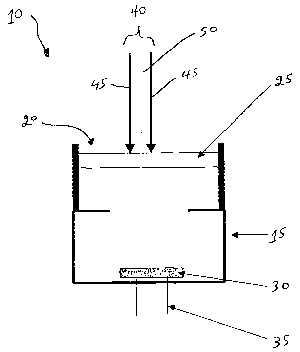
BRIEF DESCRIPTION OF THE DRAWINGS
Embodiments of the present invention will be described with reference to
the accompanying drawings, wherein lilce numerals designate like elements, and
in
which:
6
CA 02540589 2006-03-29
WO 2005/031288 PCT/CA2004/001701
Figure 1 illustrates a schematic of a radiation sensor device in accordance
with the preferred embodiment of the present invention;
Figure 2 illustrates a more detailed view of a particular embodiment of the
present radiation sensor device;
Figure 3 illustrates a schematic of use of the radiation sensor device of
Figure 1 in a fluid treatment system.
DETAILED DESCRIPTION OF THE PREFERRED EMBODIMENTS
A first element of the present radiation sensor device is an optical filter
interposed between the entrance and the radiation detector, the optical filter
having:
l0 (i) an optical transmittance of at least about 40% at a wavelength in the
range of from
about 175 nm to about 300 nm, and (ii) an optical transmittance of no greater
than
about 5% at a wavelength of greater than about 350 nm.
A suitable optical filter for use in the present radiation sensor device is
described in Knapp referred to above.
Preferably, the optical filter has an optical transmittance of at least about
70% at a wavelength in the range of from about 175 nm to about 300 nm. More
preferably, the optical filter has an optical transmittance of at least about
80% at a
wavelength in the range of from about 175 nm to about 300 nm.
Preferably, the optical filter has an optical transmittance of no greater than
2o about 5% at a wavelength in the range of from about 350 to about 1140 mn.
More
preferably, the optical filter has an optical transmittance of no greater than
about 5%
at a wavelength in the range of from about 350 to about 580 nm. More
preferably, the
optical filter has an optical transmittance of no greater than about 5% at a
wavelength
in the range of from about 1000 nm to about 1140 nm. Even more preferably, the
optical filter has an optical transmittance of no greater than about 5% at a
wavelength
in the range of from about 350 to about 580 nm and in the range of from about
1000
nm to about 1140 nm. Even more preferably, the optical filter has an optical
transmittance of no greater than about 1 % at a wavelength in the range of
from about
350 to about 580 nm and in the range of from about 1000 nm to about 1140 nm.
Even
7
CA 02540589 2006-03-29
WO 2005/031288 PCT/CA2004/001701
more preferably, the optical filter has an optical transmittance of no greater
than about
2% at one or more of the following wavelengths: 313 nm, 365 nm, 405 nm, 436 nm
546 nm, 579 nm and 1015 nm. Most preferably, the optical filter has an optical
transmittance of no greater than about 2% at each of the following
wavelengths: 313
nm, 365 nm, 405 nm, 436 nm 546 nm, 579 nm and 1015 nm.
Preferably, the optical filter further comprises a supplementary filter,
which blocks radiation having a wavelength in the range of from about 600 to
about
950 nm. The provision of such a supplementary filter is particularly useful
when the
radiation being sensed emanates from a medium pressure ultraviolet radiation
lamp or
l0 source. If present it is preferred that the supplementary filter has an
optical
transmittance of no greater than about 5%, more preferably no greater than
about 1%,
most preferably no greater than about 0.1%, at a wavelength in the range of
from
about 600 nm to about 950 nm.
Preferably, the optical filter comprises a substrate and a coating (or
coatings) having the prescribed transmittance properties. Non-limiting
examples of
suitable substrate materials may be selected from the group comprising glass,
plastic,
fused silica, sapphire and metal. In one preferred embodiment, the substrate
comprises fused silica. In another preferred embodiment, the substrate
comprises
ultraviolet radiation transparent glass.
2o The coating may present as one or more layers. Preferably, the coating
comprising a plurality of layers.
Preferably, the coating comprises one or more of Si02, A1203, SiO,
fluorides such as barium fluoride and lanthanum fluoride, MgO, Ti02, Zr02,
Ta205,
Hf02 and mixtures thereof.
Thus, in the event that radiation have at least one wavelength in the range
of from about 600 to about 950 nm impinges on the sensor device, a
supplementary
filter element which blocks radiation in this wavelength range can be
employed. Such
an additional filter element can comprise an additional series of coatings
similar to
those employed by Knapp and described above, or a more conventional filter
such as
a metal-dielectric-metal UV bandpass filter. This additional filter element
could
advantageously be placed between the first filter element and the radiation
detector,
s
CA 02540589 2006-03-29
WO 2005/031288 PCT/CA2004/001701
recognizing that some of the ultraviolet radiation has already been filtered
by the
radiation resistant first filter element and therefore does not impinge on the
additional
filter element. Alternatively, this additional filter element could disposed
above the
first filter element or incorporated in the first filter element.
A second element of the present radiation sensor device is a radiation
detector capable of detecting radiation have at least one wavelength in the
range of
from about 125 nm to about 1100 nm, the radiation detector comprising: (i) a
silicon-
containing material comprising an n-doped layer disposed on a pair of p-doped
layers,
and (ii) a passivation layer disposed on a radiation impingement surface of
the silicon
1o containing material, the passivation layer comprising nitrided silicon
dioxide (e.g., a
combination of Si3N4 and Si02), a metal silicide and mixtures thereof. More
information about such a radiation sensor device may be obtained from Canfield
et al.
in Metf°ologia 35, 1998, pg. 329 - 334.
Preferably, in the radiation detector, the n-doped layer is thinner than the
p-doped layers. More preferably, the radiation detector comprises a p-doped
substrate
on which is disposed a relatively thin n-doped layer. Most preferably, the
radiation
detector comprises, in successive layers: a p-doped substrate (bottom), a
relatively
thin p-doped layer and a relatively thin n-doped layer (top).
In one embodiment of the present radiation sensor device, the optical filter
2o is in the form of a coating (or coatings) having the prescribed
transmittance properties
and being disposed on a surface of the radiation detector.
With reference to Figure 1, there is shoran a schematic of a radiation
sensor device in accordance with the preferred embodiment of the present
invention.
Radiation sensor device 10 comprises a housing 15 having an entrance 20.
Disposed
in entrance 20 is an optical filter 25 having the transmittance properties
described
above. Disposed in housing 15 is a photodiode 30 (or other sensing element)
having
the properties described above. A pair of electrical connections 35 is
connected to
photodiode 30.
In operation of radiation sensor device 10, polychromatic radiation 40
3o passes through entrance 20 and impinges on optical filter 25. Radiation 45
having a
wavelength outside the range of from about 100 nm to about 300 nm does not
pass
9
CA 02540589 2006-03-29
WO 2005/031288 PCT/CA2004/001701
through optical filter 25. Radiation 50 having a at least one wavelength in
the range
of from about 100 nm to about 300 nm (preferably from about 240 to about 300
run
for disinfection and/or from about 175 to about 300 nm for treatment of
chemical
contaminants) passes through optical filter 25 and impinges on photodiode 30.
Importantly, if an optical filter such as the one described in Knapp is used
in the present radiation sensor device, radiation having the wavelength in the
range of
from about 600 nm to about 950 nm may pass there through as shown in Figure 11
of
Knapp. This problem is obviated or mitigated in the present radiation sensor
device
owing to the additional optional filter element incorporated into optical
filter 25.
1o As radiation having a wavelength of interest impinges on photodiode 30, it
may be detected and a corresponding signal sent to conventional electronics in
the art
to sense and/or control radiation output.
Figure 2 provides a more detailed illustration of a particular embodiment
of the present radiation sensor device showing placement of the radiation
detector and
the optical filter in relation to washers, seals and the like conventional art
used to
construct submersible devices.
The present radiation sensor device may be incorporated in an ultraviolet
radiation fluid treatment (e.g., disinfection) system. After sensing
radiation, the
output of the radiation sensor device may be used to control the ultraviolet
radiation
2o sources thereby maintaining irradiance of the ultraviolet radiation in the
disinfection
wavelength range needed to kill or otherwise inactivate harmful organisms in
the fluid
being treated. A schematic of a basic disinfection system using the present
radiation
sensor device is shown in Figure 3.
Thus, with reference to Figure 3, device 10 detects ultraviolet radiation
having at least one wavelength in the range of about 175 nm to about 300 nm
emitted
by a nearby radiation source. Device 10 then sends signal to the controller
which
adjusts the power to the ultraviolet light source so that the irradiance of
light in the
disinfection wavelength range is maintained at a desired level. Fluid passes
through
the fluid disinfection chamber of the fluid treatment system wherein harmful
organisms are killed or otherwise inactivated by the ultraviolet radiation.
Similarly, a
chemical contamination removal system with a schematic as shown in Figure 3
can be
to
CA 02540589 2006-03-29
WO 2005/031288 PCT/CA2004/001701
constructed. The output of the radiation sensor device is used to maintain the
irradiance of ultraviolet radiation needed to reduce the concentration of
chemical
contaminants in the fluid.
While this invention has been described with reference to illustrative
embodiments and examples, the description is not intended to be construed in a
limiting sense. Thus, various modifications of the illustrative embodiments,
as well
as other embodiments of the, invention, will be apparent to persons skilled in
the art
upon reference to this description. It is therefore contemplated that the
appended
claims will cover any such modifications or embodiments.
l0 All publications, patents and patent applications referred to herein are
incorporated by reference in their entirety to the same extent as if each
individual
publication, patent or patent application was specifically and individually
indicated to
be incorporated by reference in its entirety.
11