Note : Les descriptions sont présentées dans la langue officielle dans laquelle elles ont été soumises.
CA 02541524 2006-04-04
WO 2005/040450 PCT/US2004/032861
METHOD AND APPARATUS FOR COATING AN ORGANIC THIN FILM
ON A SUBSTRATE FROM A FLUID SOURCE WITH CONTINUOUS
FEED CAPABILITY
This invention was made with U.S. Government support under Contract
DE-AC0676RL01830 awarded by the U.S. Department of Energy. The U.S.
Government has certain rights in the invention.
zo Cross-Reference To Related Applications
Not Applicable
Background Of The Invention
As a result of the broad use of thin films across a wide variety of industrial
15 applications, a tremendous amount of research has been conducted towards
the
development of various types of thin films and methods for manufacturing them
in a cost
effective manner. One such type of thin film is the small molecule organic
semiconductors, which are currently under development for a number of
applications,
including displays, transistors and memories. One particular area of interest
for these
2o materials is the application of organic light emitting devices ("OLEDs")
for interior room
lighting. Proof of principle experiments have shown that OLEDs can operate at
as high
as 60 lm/W. Although this record is at low brightness and for a green device,
it stands
as evidence that large area lighting at this efficiency is scientifically
feasible. Indeed, this
result was obtained in a planar device geometry from which only ~ 20% of the
photons
25 generated in the device escape to an observer, thus demonstrating that the
theoretical
upper limit for device efficiency is at least 300 lm/W in the green. Other
areas of
application are in Large area, very low cost electronics based on organic thin
films
transistors and low cost, large area photovoltaics.
Despite the promise of energy efficient lighting presented by these materials,
a
3o high quality, low cost, high throughput deposition system for these
materials does not
currently exist. Conventional physical vapor deposition techniques or spin
coating,
-1-
CA 02541524 2006-04-04
WO 2005/040450 PCT/US2004/032861
although effective for small area, high value-added applications, axe too slow
to be viable
for the production of low cost lighting. Organic vapor phase deposition using
low
vacuum and shower-head type geometries derived from the chemical vapor
deposition
industry have not proven capable of the high deposition rates required for
roll-to-roll
fabrication. Printing techniques are also too slow and generally restricted to
batch
manufacturing. A high throughput, continuous feed, roll-to-roll deposition
technique for
small molecule semiconductors is thus likely the only viable route to high
volume
production of OLED lighting panels with a cost of ov~niership competitive with
conventional lighting solutions.
to Polymer multilayer deposition (PML) is a well-known technique for the high
speed deposition of extremely uniform thin films of acrylate-based polymers.
In general,
the PML process has two forms - evaporative and non-evaporative. Each begins
by
degassing the working monomer, which is a reactive organic liquid. In the
evaporative
process, the monomer is metered through an ultrasonic atomizer into a hot tube
where it
15 flash evaporates and exits through a nozzle as a monomer gas. The monomer
gas then
condenses on the substrate as a liquid film that is subsequently cross-linked
to a solid
polymer by exposure to UV radiation or an electron beam. W the non-evaporative
process, the degassed liquid monomer is extruded through a slotted die orifice
onto the
substrate. It is then cross-linked in the same fashion as in the evaporative
process. Salts,
2o graphite or oxide powders, and other nonvolatile materials can be deposited
in a
homogeneous mixture with the monomer. Such mixtures cannot be flash
evaporated, but
are required for electrolyte, anode, cathode, and capacitor film layers. The
evaporative
process has been shown to produce thicknesses up to approximately 10 microns
at speeds
as great as 1000 feet per minute. The non-evaporative process have been shown
to
25 deposit thicknesses from 10 microns to about 50 mils at substrate speeds
approaching
several hundred feet per minute. Various aspects of the PML processes are
described in
greater detail in the following US patents, the entire contents of each of
which are hereby
incorporated herein by this reference: 6,613,395 Method of making molecularly
doped
composite polymer material, 6,570,325 Environmental barrier material fox
organic light
3o emitting device and method of making, 6,544,600 Plasma enhanced chemical
deposition
of conjugated polymer, 6,522,067 Environmental barrier material for organic
light
emitting device and method of making, 6,509,065 Plasma enhanced chemical
deposition
of conjugated polymer, 6,506,461 Methods for making polyurethanes as thin
films,
_2-
CA 02541524 2006-04-04
WO 2005/040450 PCT/US2004/032861
6,497,924 Method of making non-linear optical polymer, 6,497,598 Environmental
barrier material for organic light emitting device and method of making,
6,358,570
Vacuum deposition and curing of oligomers and resins, 6,274,204 Method of
making
non-linear optical polymer, 6,268,695 Environmental barrier material for
organic light
emitting device and method of making, 6,228,436 Method of making light
emitting
polymer composite material, 6,228,434 Method of making a conformal coating of
a
microtextured surface, 6,224,948 Plasma enhanced chemical deposition with low
vapor
pressure compounds, 6,217,947 Plasma enhanced polymer deposition onto
fixtures,
6,207,239 Plasma enhanced chemical deposition of conjugated polymer, 6,207,238
l0 Plasma enhanced chemical deposition for high and/or low index of refraction
polymers,
5,902,641 Flash evaporation of liquid monomer particle mixture, 5,681,615
Vacuum
flash evaporated polymer composites, 5,547,508 Vacuum deposition and curing of
liquid monomers apparatus, 5,395,644 Vacuum deposition and curing of liquid
monomers, 5,260,095 Vacuum deposition and curing of liquid monomers.
Unfortunately, the polymeric materials amenable to PML deposition are
electrically inert, and although it is possible to incorporate guest molecules
into the PML
flux, it is difficult to achieve a high enough loading of active material to
realize an
electrically active device such as an efficient, low voltage OLED.
Furthermore, the
evaporative mode of PML which is generally used to make films of an
appropriate
thickness for electronics devices, the guest molecules tend to fractionate out
into the flash
evaporation box where they accumulate, rather than being deposited on the
target
substrate. One similar approach is described in US Patent 6,471,327, the
entire contents
of which axe incorporated herein by this reference. As described by the '327
patent, an
apparatus and method of focusing a functional material includes a pressurized
source of
fluid in a thermodynamically stable mixture with a functional material. A
discharge
device having an inlet and an outlet is comiected to the pressurized source at
the inlet.
The discharge device is shaped to produce a collimated beam of functional
material,
where the fluid is in a gaseous state at a location before or beyond the
outlet of the
discharge device. The fluid can be one of a compressed liquid and a
supercritical fluid.
3o The thermodynamically stable mixture includes one of the functional
material being
dispersed in the fluid and the functional material being dissolved in the
fluid. Drawbacks
associated with the approach of the '327 patent include issues related to
handling a
highly pressurized fluids, such as a supercritical fluids. Accordingly, to
solve the
-3-
CA 02541524 2006-04-04
WO 2005/040450 PCT/US2004/032861
manufacturing problems associated with low cost or Iarge area electronics, a
need exists
for a technique with similar characteristics to PML, but which is useful for
organic
semiconductors and which avoids the problems associated with gasses under high
pressure.
Brief Summary Of The Invention
Accordingly, it is an object of the present invention to provide a method for
coating a
thin film of a non-polymeric compound on a substrate. The method of the
present
invention is different from PML in several key ways. One such key difference
is related
to the difference between PML coatings, which are generally made up of monomer
or
1o oligomer materials which are readily delivered in a liquid form to an
ultrasonic nozzle
directed into a flash evaporation box, and the non-polymeric compounds which
ultimately form the coatings of the present invention, such as, by way of
example,
organic semiconductors. The coatings of the present invention are mostly
solids at room
temperature and many sublime without passing through a liquid phase and are
therefore
15 not readily evaporated in the manner PML coatings are evaporated. A second
key
difference is that the PML coatings use a monomeric or oligomeric starting
material but
the deposited film is typically polymeric or rendered polymeric by treatment
on the
substrate shortly after deposition, whereas the coatings of the present
invention axe
chemically substantially similar to the starting materials. To overcome these
differences,
2o the present invention provides a mixture of the non-polymeric compound and
a fluid
carrier. The mixture typically consists of a slurry of the non-polymeric
compound in the
fluid carrier. However, the mixture may have all or a portion of the non-
polymeric
compound in solution in the fluid carrier, or as a colloidal suspension in the
carrier, or
combinations thereof. As used here, the term "mixture" should be broadly
construed to
25 contemplate all of these possibilities. This mixture is then pumped into
the interior of a
heated evaporation box having an internal temperature sufficient to convert
substantially
all of the non-polymeric compound and fluid carrier to a gaseous form. The non-
polymeric compound and fluid carrier are then removed from the evaporation box
via an
exit slit in the evaporation box. Adjacent to the exit slit, and maintained in
a vacuum, is
3o a substrate upon which the non-polymeric compound condenses. The substrate
is in
motion relative to the evaporation box, for example on a web roller, thereby
allowing a
continuous coating of the non-polymeric compound to be applied to the
substrate.
-4-
CA 02541524 2006-04-04
WO 2005/040450 PCT/US2004/032861
Typically, the substrate is maintained at a temperature sufficiently high 'so
that the
fluid carrier does not condense on the substrate, thus allowing the formation
of a coating
of the non-polymeric coating free of any of the fluid carrier. However, this
objective can
also be accomplished by maintaining the substrate at a temperature
sufficiently high so
that any fluid carrier that might initially condense upon contact with the
substrate quickly
evaporates. Alternatively, by maintaining the substrate at a temperature
sufficiently low
to allow both the fluid carrier and the non-polymeric compound to condense on
the
substrate at the exit slit of the evaporation box, and subsequently increasing
the
temperature of the substrate to a temperature sufficient to cause the fluid
corner to
1o evaporate, a coating of the non-polymeric compound free of any of the fluid
carrier is
likewise formed. The preferred mode of operation is likely to depend on the
organic
compound being evaporated and/or the desired morphology of the deposited film
(i.e.
crystalline or amorphous).
Under either approach, the goal is to produce a coating of the non-polymeric
material
15 substantially free of any of the fluid carrier. W this manner, the fluid
carrier may be
captured, allowing the subsequent use of the fluid carrier to provide
additional mixture of
the non-polymeric compound with the fluid carrier. Capturing the fluid carrier
is easily
accomplished by providing a cold trap to condense the fluid carrier.
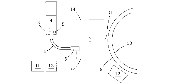
A suitable apparatus for the process is shown in Fig. 1. As shown in the
figure, the
2o mixture of the non-polymeric compound aazd fluid carrier 1 is maintained in
a reservoir 2
having a syringe pump 4. Within reservoir 2 preferably has a means 3 for
agitating the
mixture, including but not limited to an ultrasonic agitation, mechanical
vibration, and
magnetic stirnng, employed to maintain the mixture as homogeneous. When pump 4
is
pushed, the mixture 1 is directed down capillary 5, preferably towards an
ultrasonic tip,
25 or fuel injector 6. Mixture 1 is thereby injected into evaporation box 7
through the
ultrasonic tip, or fuel injector 6 in an atomized form. The interior of the
evaporation box
7 is maintained at a temperature sufficient to maintain the non-polymeric
compound and
the fluid carrier in a gaseous state by a heating means. While not meant to be
limited, the
heating means could include resistive coils 14 as shown in the figure.
Evaporated fluid
3o carrier and non-polymeric compound 1 exits the evaporation box 7 through an
exit slit 8
whereupon the non-polymeric compound is preferably condensed upon a moving
substrate 9. While not meant to be limiting, the moving substrate may be
provided on a
_5_
CA 02541524 2006-04-04
WO 2005/040450 PCT/US2004/032861
web roller 10. The moving substrate may be rigid such as a glass plate or
flexible such
as a plastic or metal foil. The web roller is maintained in a vacuum, created
with a pump
11. As noted above, the fluid earner may be captured, allowing the subsequent
use of the
fluid carrier to provide additional mixture of the non-polymeric compound with
the fluid
carrier, by providing a cold trap 12 in front of a pump. A plasma source 13
may
optionally be employed to treat the substrate, thereby cleaning the substrate
and
improving the adhesion of layers deposited thereupon. The exit slit of the
evaporation
box may also be provided as a series of exit slits, as shown in Fig. 2.
To fully evaporate the non-polymeric compound and the fluid earner, the
evaporation
1o box temperature is preferably provided as greater than 100°C. The
important criterion is
that the box be hot enough to evaporate the entire fluid flux entering and be
provided
with sufficient energy that such temperature is maintained at the desired rate
of fluid
input. In this mode, the deposition rate on the substrate depends not on the
temperature of
the evaporation box but only on the fluid pump speed and the condensation
efficiency on
15 the substrate. Also, mixtures can be employed, for example, and not meant
to be limiting,
a doped light emitting layer consisting of 4% fac-tris(2-
phenylpyridine)iridium in 4,4'-
N,N'-dicarbazole-biphenyl, the emissive layer for a green phosphorescent OLED,
could
be deposited by starting from an intimately ground mixture of the component
materials in
a fluid carrier with the evaporation box maintained at such a temperature so
as to
2o evaporate both components and the fluid. This improves on the most commonly
used
technique to produce doped films of small molecule organic semiconductors
where two
spatially separated sources are individually heated in a high vacuum chamber
with the
rate of deposition of each material being controlled by the temperature of its
respective
source. The problem is that the evaporation rate is to first order
exponentially dependent
25 on the source temperature so very accurate temperature control is required.
In the present
invention, the evaporation box is only required to be maintained above a
minimum
temperature and the composition of the deposited film is substantially
determined by the
composition of the starting mixtuxe.
The non-polymeric compound may be selected as an organic material, including
but not
30 limited to OLED materials such as a metal (8-hydroxyquinoline) chelate, or
inorganic
materials, or mixtures thereof. It is important to note that as used herein
the term "non-
polymeric" simply means that the compound that is provided in the mixture is
-6-
CA 02541524 2006-04-04
WO 2005/040450 PCT/US2004/032861
substantially the same as the compound that is ultimately applied to the
substrate; ie. it
has not been polymerized, as is typical in the PML process. Notably, some
monomers
which are capable of polymerization, but which are nevertheless NOT
polymerized
during the deposition process, would therefore qualify as "non-polymeric"
compounds as
that teen is used herein. Oligomers also would be included, as per TLTFAC
definitions.
Suitable OLED materials, together with OLED fabrication techniques and
suitable
structures for mufti-layer materials utilizing OLEDs, have been described in
great detail
in the patent literature. Suitable OLEDs are described in the following US
Patents, the
entire contents of each of wluch are hereby incorporated herein by this
reference:
6,613,395 "Method of Making Molecularly Doped Composite Polymer Material"
(2003), 6,602,540 "Fabrication of non-polymeric flexible organic light
emitting devices."
(2003), 6,596,134 "Method of Fabricating Transparent Contacts for Organic
Devices."
(2003), 6,582,838 "Red-emitting organic Iight emitting devices (OLED's)."
(2003),
6,579,632 "OLEDs doped with phosphorescent compounds." (2003), 6,570,325
"Environmental Barrier Material fox Organic Light Emitting Device and Method
of
Making." (2003), 6,558,736 "Low pressure vapor phase deposition of organic
thin
films." (2003), 6,548,956 "Transparent contacts for organic devices." (2003),
6,497,924
"Method of Making a Nonlinear Optical Polymer." (2002), 6,469,437 "Highly
Transparent Organic Light Emitting Devices Employing a Non-Metallic Cathode"
2o (2002), 6,468,819 "Method for Patterning Organic Thin Film Devices Using a
Die
(2002), 6,451,455 "Metal Complexes Bearing Both Electron Transporting and Hole
Transporting Moieties" (2002), 6,420,031 "Highly Transparent Non-Metallic
Cathodes"
(2002), 6,403,392 "Method for Patterning Devices" (2002), 6,396,860 "Organic
Semiconductor Laser." (2002), 6,365,270 "Organic Light Emitting Devices"
(2002),
6,358,631 "Mixed Vapor Deposited Films for Electroluminescent Devices"(2002),
6,337,102 "Low Pressure Vapor Phase Deposition of Organic Thin Films." (2002},
6,329,085 "Red-Emitting Organic Light Emitting Devices (OLEDs)" (2001),
6,330,262
"Organic Semiconductor Lasers" (2001), 6,303,238 "OLEDs doped with
phosphorescent compounds" (2001), 6,297,516 "Method for Deposition and
Patterning
of Organic Thin Film." (2001}, 6,294,398 "Method for Patterning Devices."
(2001),
6,274,980 "Single Color Stacked Organic Light Emitting Device." (2001),
6,264,805
"Method of Fabricating Transparent Contacts for Organic Devices." (2001),
6,232,714
"Saturated Full Color Stacked Organic Light Emitting Devices." (2001),
6,214,631
_7_
CA 02541524 2006-04-04
WO 2005/040450 PCT/US2004/032861
"Method for Patterning Light Emitting Devices Incorporating a Movable Mask."
(2001),
6,160,828 "Organic Vertical-Cavity Surface-Emitting Laser." (2000), 6,125,226
"Light
Emitting Devices Having High Brightness." (2000), 6,111,902 "Organic
Semiconductor
Laser." (2000), 6,097,147 "Structure for High Efficiency Electroluminescent
Device."(2000), 6,091,195 "Displays Having Mesa Pixel Configuration." (2000),
6,048,630 "Red-Emitting Organic Light Emitting Devices (OLEDs) (2000),
6,046,543
"High Reliability, High Efficiency, Integratable Organic Light Emitting
Devices and
Methods of Producing Same" (2000), 6,045,930 "Materials fox Multicolor Light
Emitting
Diodes" (2000), 6,030,715 "Azlactone-Related Dopants in the Emissive Layer of
an
to OLED" (2000), 6,030,700 "Organic Light Emitting Devices" (2000), 6,013,538
"Method
of Fabricating and Patterning OLEDs" (1999), 6,005,252 "Method and Apparatus
for
Measuring Film Spectral Properties" (1999), 5,998,803 "An Organic Light
Emitting
Device Containing a Hole W jection Enhancement Layer" (1999), 5,986,401 "High
Contrast Transparent Organic Light Emitting Device Display" (1999), 5,981,306
"Method for Depositing Indium Tin Oxide Layers in Organic Light Emitting
Devices"
(1999), 5,986,268 "Organic Luminescent Coating for Light Detectors" (1999),
5,953,587
"Method for Deposition and Patterning of Organic Thin Film" (1999), 5,917,280
"Stacked Organic Light Emitting Devices" (1999), 5,932,895 "Saturated Full
Color
Stacked Organic Light Emitting Devices" (1999), 5,874,803 "Light Emitting
Device with
2o Staclc of OLEDs and Phosphor Downconverter" (1999), 5,861,219 "Organic
Light
Emitting Devices Containing a Metal Complex of 5-Hydroxy-Quinoxaline As a Host
Material" (1999), 5,844,363 "Vacuum Deposited Non-Polymeric Flexible Organic
Light
Emitting Devices" (1998), 5,834,893 "High Efficiency Organic Light Emitting
Devices
with Light Directing Structures" (1998), 5,757,139 "Driving Circuit for
Staclced Organic
Light Emitting Devices" (1998), 5,757,026 "Multicolor OLED" (1998), 5,721,160
"Multicolor Organic Light Emitting Devices" (1998), 5,707,745 "Multicolor
Organic
Light Emitting Devices" (1998), 5,703,436 "Transparent Contacts for Organic
Devices"
(1997), 5,554,220 "Method and Apparatus Using Organic Vapor Phase Deposition
for
the Growth of Organic Thin Films with Large Optical Non-Linearities" (1996).
As will
3o be recognized by those having skill in the art, in addition to the
manufacture of light
emitting devices, the present invention is readily applicable to the
manufacture of thin
film transistors, photovoltaic devices and other devices and products
requiring a thin
coating of an organic material.
_g_
CA 02541524 2006-04-04
WO 2005/040450 PCT/US2004/032861
The fluid carrier is preferably a fluid that will readily evaporate at the
preferred
temperature of the evaporation box, and which condenses at a temperature
higher than
the condensation temperature of the non-polymeric compound. Suitable fluid
carriers
include, but are not limited to straight chain and branched alcohols and
diols, amides,
dimethylsulfoxide, N-methylpyrrolidinone, toluene, ketones, esters,
halogenated
solvents, and combinations thereof.
Brief Description Of The Several Views Of The Drawina_
FIG. 1 is a schematic drawing showing a preferred embodiment of the present
invention used to perform proof of principle experiments.
l0 FIG. 2 is a schematic drawing showing a preferred embodiment of the present
invention showing multiple slits in an evaporation box.
FIG. 3 is a photograph showing the film resulting from proof of principle
experiments described in the Detailed Description of the Preferred Embodiment
section
below.
Is Detailed Description of a Preferred Embodiment
An experiment was conducted to demonstrate one preferred embodiment of the
present invention. An apparatus as described above and shown in Figure 1 was
fashioned by modifying an existing PML system, thereby allowing the transport
and
20 subsequent deposition of small molecule organic semiconductors in a solvent
earner. A
syringe ptunp functioned as the source reservoir, which supplies the
organic/solvent
mixture at constant flow to an injector which atomized the mixture into an
evaporation
box. The temperature of the evaporation box was sufficient to insure that the
entire
mixture was vaporized at a sufficient rate to ensure no build-up of material
in the box.
25 The vapor stream exited through a slit and was directed onto a moving web,
the
temperature of which is controlled such that only the desired organic
semiconductor
deposited as a solid film, and the solvent either did not deposit or quickly
evaporated and
was pumped out of the deposition chamber. In these proof of principle
experiments, thin
films of the archetypal organic light emitting semiconductor, aluminum (8-
30 hydroxyquinoline) chelate (Alq3), Were first formed into a slurry by
grinding with a
mortar and pestle and then mixing with 1-hexanol with ultrasonic agitation.
Loading of
-9-
CA 02541524 2006-04-04
WO 2005/040450 PCT/US2004/032861
the Alq3 in the 1-hexanol was approximately 30% by weight. Bilayer organic
light
emitting devices were fabricated using two separate passes through the system.
The
substrate was 7 inches across, and was passed through the system at speeds of
up to
approximately 10 feet per minute, although much faster speeds are possible.
The web
temperature was maintained at between 70 and 90°F. For these proof of
principle
experiments, the temperature in the evaporation box was maintained at between
500 and
700°F. The syringe pump delivered the mixture at between 0.11 & 1.65
ml/minute.
Pressure within the pump was maintained at between 5 and 15 psi, and the
capillary
between the pump and the evaporation box was 30 mil id reduced to 20 mil id to
to maintain back pressure in the pump. While this diameter worked for the
specific
pressure regime and mixture used for these experiments, those having skill in
the art will
recognize that a suitable size that will prevent back pressure in the pump
will depend on
the viscosity of the mixture, and will select capillaries accordingly. The
vacuum
surrounding the web roller was maintained at between 10-5 and 10-4 tort.
Electrodes were
applied using a conventional vacuum thermal deposition system and the
resulting devices
were observed to emit light in response to an inj ected current. An example of
the films
produced by these experiments is shown in Figure 3.
In manufacturing versions of the process, the solvent could be recovered for
recycling. The solvent used in this demonstration was 1-hexanol, and the non-
polymeric
compound was Alq3, but it should be noted that 1-hexanol is a poor solvent for
AIq3 and
the mixture is mostly a fine slurry (made by grinding and ultrasonic
agitation) rather than
a clear solution. This is acceptable for the process as long as the slurry
does not clog the
feed system; the role of the solvent is only as a rechargeable, continuous
feed fluid
source arid it is designed so as not to be incorporated in the deposited thin
film. Desirable
characteristics of the solvent are a sufficiently high vapor pressure to cause
minimal
incorporation into the deposited films and the correct viscosity to transport
well through
the feed system under positive pressure (i.e. flow- controlled rather than
temperature-
controlled).
3o Alternative embodiments of the present invention would include, but are not
limited to, a continuous feed system based on the above design where two or
more fluid
source reservoirs were switched by means of a mufti-way valve. The temperature
of the
evaporation box is controlled so that everything entering as a fluid exits as
a vapor,
-l0-
CA 02541524 2006-04-04
WO 2005/040450 PCT/US2004/032861
therefore film thickness is flow-controlled, not temperature-controlled. Doped
films are
also possible, with very accurate control over the doping ratio by premixing
the dopant in
the fluid reservoir rather than the current method used in thermal evaporation
systems of
independently controlling two or more thermal evaporation sources. Since the
evaporation rate in thermal sublimation systems is exponentially dependent on
temperature, accurate doping control is difficult. The present invention
therefore
overcomes this drawback.
If premixing is for some reason proscribed, more than one metered source can
io feed the same evaporation box at independently controlled rates either via
separate
atomizers, or by routing both sources into the same atomizer.
The distance from the slit to the substrate can be adjusted within the limits
set by
the geometry of the deposition system, but that with suitable optimization of
the slit size,
15 flow rate, temperature (and hence pressure in the box) good uniformity
across a very
long exit slit can be obtained even at close slit to substrate distances (i.e.
1 cm or less).
This leads to the embodiment shown in Fig. 2, where multiple exit nozzles are
used to
achieve coarse patterning of the organic semiconductor in a technique
analogous to (but
distinct from) inkjet printing. Micron-scale nozzles fabricated using
microfluidic
2o techniques eould yield micron-scale patterned film deposition on the
substrate. In yet
another embodiment, each nozzle could be connected to a distinct source
reservoir and be
controlled at a separate temperature permitting, for example, the simultaneous
deposition
of red, blue and green light emitting layers on a moving web or, for
transistor
applications, p, n and metallic organic materials for heterogeneous
integration of organic
25 electronic circuitry. Lateral fitter in the substrate position could be
used to sharpen the
Gaussian lineshape expected at the edge of each pattern and a small shutter
installed over
each nozzle could provide for patterning in the direction of substrate
transport.
CLOSURE
3o While a preferred embodiment of the present invention has been shown and
described, it will be apparent to those skilled in the art that many changes
and
modifications may be made without departing from the invention in its broader
aspects.
-11-
CA 02541524 2006-04-04
WO 2005/040450 PCT/US2004/032861
The appended claims are therefore intended to cover all such changes and
modifications
as fall within the true spirit and scope of the invention.
-12-