Note : Les descriptions sont présentées dans la langue officielle dans laquelle elles ont été soumises.
CA 02541977 2006-04-06
WO 2005/044499 PCT/US2004/027339
VERTICAL REMOVAL OF EXCESS SOLDER FROM A CIRCUIT
SUBSTRATE
FIELD OF THE INVENTION
This invention in general relates to printed circuit substrates and, more
particularly, to preventing solder defects on reworked printed circuit
substrates.
BACKGROUND OF THE INVENTION
Printed circuit substrates are employed in the electronic industry for the
placement and interconnection of electronic circuits. Examples of printed
circuit
substrates in use in the electronic industry include: ceramic substrates,
printed circuit
boards, flexible printed circuits, porcelain-on-metal substrates, and silicon-
on-silicon
substrates. These electronic circuits may comprise expensive microprocessor or
digital signal processor circuitry in large packages requiring many pinouts to
connect
to the printed circuit substrate. For example, a ball-grid array (BGA) package
may be
used for such circuitry. These BGA packages are typically electrically
connected to a
printed circuit substrate by a surface mounting technique, such as a mass
solder
reflow operation using hot air or other hot gas such as nitrogen.
The BGA package in particular causes some manufacturing difficulty as the
solder connections from the printed circuit substrate to the BGA pinouts are
directly
beneath the BGA package. Therefore, standard solder wave reflow technique can
not
be used as the solder can not move beneath the package to make the
connections.
Moreover, the density of these connections can be quite large results in a
very small
pitch between connections which can result in solder bridging that
electrically shorts
connections together. As a result, special assembly techniques must be used
that can
CA 02541977 2006-04-06
WO 2005/044499 PCT/US2004/027339
2
include solder balls, printed solder paste, or solder bumps pre-placed on the
circuit
substrate and spaced apart by a solder mask. The BGA package is then placed on
the
paste, solder bumps or balls, and the assembly is heated using hot air or
other hot gas
such as nitrogen to melt the solder in order to connect the BGA pinouts to the
printed
circuit substrate connections. While most BGA attach and repair techniques use
hot
air to melt the solder, for single sided assemblies, sometimes a hot plate or
heated
cartridge under the circuit substrate is used to melt the solder. Other means
of locally
heating the circuit substrate that have been used to locally melt solder
include:
infraxed radiation, soft beam light energy, laser light energy, and applying a
hot
condensing vapor such as fluorinert (as is used in vapor phase reflow
systems).
The problem becomes worse in the removal of defective BGA packages, in
that, the removal process typically involves repeating the solder connection
and
carefully removing the BGA device. If the BGA device is not lifted off the
board
properly (i.e. a lateral movement occurs) solder bridging can occur requiring
further
recovery measures or the scrapping of the circuit substrate. In addition, the
solder
mask used between connections is delicate and flexible and can be damaged if
any
lateral movement occurs in the removal of the BGA package. If the solder mask
is
damaged the re-installation of a new BGA device on the reworked circuit
substrate
can easily result in a new solder bridge, which then requires further rework.
Prior art methods include using a cutting wire to remove the package and the
use of high-pressure water jets. However, these mechanical techniques will
definitely
cause damage to the solder mask. Reflowing the solder to remove the part is
least
damaging to the solder mask. However, there may be an excessive amount of
residual
solder left over after the removal of the BGA package, which requires further
rework
CA 02541977 2006-04-06
WO 2005/044499 PCT/US2004/027339
on the circuit substrate, such as using a braided copper solder wick as is
known in the
art. This further rework can damage the solder mask, also.
Therefore, a need exists for an improved technique for the removal of excess
solder, which can result in solder bridges, from a circuit substrate without
damage to a
solder mask. It would also be desirable to provide such improvement in a
simple,
single gang operation that limits the potential for damaging lateral movement.
It
would be of further benefit to use the same equipment for connecting and for
disconnecting circuits to the printed circuit substrate, so as to make the
removal
technique economical and to maintain process control.
BRIEF DESCRIPTION OF THE DRAWINGS
The features of the present invention, which are believed to be novel, are set
forth with particularity in the appended claims. The invention, together with
further
objects and advantages thereof, may best be understood by making reference to
the
following description, taken in conjunction with the accompanying drawings, in
the
several figures of which like reference numerals identify identical elements,
and
wherein:
FIG. 1 is a cross-sectional view of a BGA device and printed circuit substrate
assembly known in the art;
FIG. 2 is a cross-sectional view of the printed circuit substrate of FIG. 1
after a
typical solder reflow removal of the BGA device;
FIG. 3 is a cross-sectional view of a sacrificial circuit substrate placed in
proximity to the excessive solder of the printed circuit substrate of FIG. 2,
in
accordance with the present invention;
CA 02541977 2006-04-06
WO 2005/044499 PCT/US2004/027339
4
FIG. 4 is a cross-sectional view of the operation of the sacrificial circuit
Substrate on the reflowed assembly of FIG. 3, in accordance with the present
invention;
FIG. 5 is a cross-sectional view of the printed circuit substrate of FIG. 4
after
removal of the sacrificial circuit substrate, in accordance with the present
invention;
and
FIG. 6 is a flow chart of a method, in accordance with the present invention.
While the invention is susceptible to various modifications and alternative
forms, specific embodiments have been shown by way of example in the drawings
and will be described in detail herein. However, it should be understood that
the
invention is not intended to be limited to the particular forms disclosed.
Rather, the
invention is to cover all modifications, equivalents and alternatives falling
within the
broad scope of the invention as defined by the appended claims.
DETAILED DESCRIPTION OF THE PREFERRED EMBODIMENTS
The present invention provides an improved technique for the removal of
excessive residual solder from a circuit substrate without damage to a solder
mask.
The present invention also provides a simple, single gang operation that
limits the
l
potential for damaging lateral movement. Moreover, the same equipment for
assembly of circuit substrates can be used for disconnecting circuits from the
printed
circuit substrate, making the present invention economical while maintaining
process
control.
CA 02541977 2006-04-06
WO 2005/044499 PCT/US2004/027339
The present invention can be useful in removing excess solder from the
rework site of any fine pitch electronic component, not just Ball Grid Arrays.
The
present invention could also be used for BGA, Micro BGA, Chip Scale Packages
(CSP), and Flip-Chip devices, as well as Fine Pitch Quad Flat Pack (QFP) and
Quad
5 Flat No-lead (QFN) packages. The present invention is configured to provide
vias to
match the footprint of the component that it will be used to rework. Typical
BGA
pads range from 27 mil diameter down to 19 mil diameter, so the via diameter
for the
present invention will be approximately 10 mils for these packages. However,
the via
diameter for this size BGA could range from 10 mils thick up to 60 mils thick.
This
size would also be typical for a QFP or QFN package. A Micro BGA package can
have pads as small as 12 mils, and so a smaller via diameter can be used. The
SCS
for this size Micro BGA could range from 10 mils thick up to 30 mils thick.
For CSP
and Flip Chip, the pads are 8 to 15 mils diameter, and the vial could be even
smaller
ranging from 5 mils thick up to 18 mils thick.
FIG. 1 shows a known assembly of an integrated circuit device 10, such as a
ball-grid array (BGA) device, to a printed circuit substrate 12. Solder 14
connects the
individual BGA pinouts 16 to respective electrical pads 18 on the printed
circuit
substratel2, which have electrical traces (not shown) that run to other
circuitry on or
off the circuit substrate as is known in the art. A solder mask 20 is present
between
the electrical pads 18. The solder mask 20 is made of a material that repels
molten
solder 14, as is known in the art. In this way, the solder mask 20 prevents
solder
bridging that can short-circuit electrical connections 16, 18, causing an
electrical
failure of the assembly requiring a rework of the assembly and hopefully the
recover
of the BGA device 10, printed circuit substrate 12, or both. However, it
should be
CA 02541977 2006-04-06
WO 2005/044499 PCT/US2004/027339
6
recognized that other common types of circuit failure can also require a
rework of the
assembly. For Flexible circuit substrate 12 the solder mask 20 must also be
flexible,
making the solder mask 20 prone to damage during rework procedures.
FIG. 2 shows a typical printed circuit substrate 12 after removal of the BGA
device. Typically, when a BGA device is soldered to a circuit substrate, over
90% of
the solder is supplied by the BGA device and less than 10% from deposited
solder
paste on the circuit substrate. As can be seen, excessive solder 14 may exist
at several
locations on the printed circuit substrate 12 after removal of a device. The
amount of
excessive solder is inconsistent but is generally about 50% of the original
amount,
where only 10% is needed for reworking purposes. The excess solder at each
location
will be of varying amounts. Although it is desirable in the re-assembly of
components to have some solder left on the electrical connections of the
printed
circuit substrate, it is not desirable to have excessive solder as this may
cause solder
bridges as explained previously. FIGS. 3-5 demonstrate a system for the
vertical
removal of excess solder from a circuit substrate to protect the solder mask,
in
accordance with the present invention.
FIG. 3 shows a sacrificial circuit substrate 30 (SCS) placed in proximity to
the
excessive solder 14 of the printed circuit substrate 12 in preparation for the
removal of
the excess solder 14. The sacrificial circuit substrate 30 includes a
plurality of
metallic pads 38. Preferably, the sacrificial circuit substrate 30 also
includes a
plurality of vial 32 connected to the pads 38. The vias can be of various
shapes but
are preferably cylindrical. Generally, the circuit substrate is made of a thin
flexible
material such as FR4, which is known in the art. The sacrificial circuit
substrate 30
can also be made of a thin flexible material such as FR4, to be conformant
with the
CA 02541977 2006-04-06
WO 2005/044499 PCT/US2004/027339
7
circuit substrate 12. However, it is preferred that the sacrificial circuit
substrate 30 be
provided in a rigid substrate such as a resin-impregnated glass weave as is
known in
the art and which is much cheaper than flexible FR4. Typically, the vies 32
are
through-holes formed through the board 30 and arranged in a pattern matching
that of
the pinout of the device that was removed. For example, a BGA package has
regularly spaced pinouts in an array formation corresponding to the locations
of the
pads 18 of the circuit substrate 12. The pads 38 and vies 32 of the
sacrificial circuit
substrate 30 would be similarly arranged in an array to align with the
plurality of
excess solder 14 bumps on the circuit substrate 12.
A portion of each pad 38 and via 32 has a solder-wettable material 34 disposed
thereon. Typically copper or copper alloy is used for the solder-wettable
material 34.
Preferably, the pads 38 and vies 32 are gold plated to maintain the integrity
of the
solder wettable properties. However, other solder-wettable materials and
alloys can
be used equally well. The vies 32 of the sacrificial circuit substrate 30
includes
through-holes 34 that are plated with a solder-wettable material. The pads 38,
and
optional vies 32 and through-holes 34 are configured to provide a desired
amount of
excess solder wicking, as will be detailed below.
Due to the uneven nature of the excess solder bumps 14, the pads 38 of the
sacrificial board 30 will not all be in contact with the excess solder bumps.
However,
once reflowed, contact will be made with all the excess solder bumps 14.
Moreover,
the alignment of the placement of the sacrificial circuit substrate 30 over
the circuit
substrate 12 is not critical as the surface tension of the reflowed solder
bumps will
serve to align the two as shown in FIG. 4.
CA 02541977 2006-04-06
WO 2005/044499 PCT/US2004/027339
8
FIG. 4 shows the operation of the sacrificial circuit substrate on the
reflowed
assembly. Specifically, the plurality of pads 38 and vias 32 of the
sacrificial circuit
substrate 30 are to be located in vertical proximity to the excess solder 14
of the
circuit substrate 12 so as to wick the excess solder vertically onto the pads
38 and vias
32, and subsequently into the through-holes 36 of the vias 32 of the
sacrificial circuit
substrate 30. A heat source 38 is provided for heating the excess solder to a
liquidous
state. Preferably, the heat source is a hot gas source, such as air or
nitrogen, to reflow
the excess solder. Reflowed solder 14 will adhere to the solder-wettable
surface 34 of
the pads 38 and vial 32, and surface tension will draw the excess solder 14
into the
vias 32 by a capillary (wicking) action. The dimensions of the vias, through-
holes
and pads are chosen, given the material of the solder-wettable surface 34,
along with
the amount and time of heat applied, in order to remove most of the excess
solder but
leaving a predetermined amount on the pads 18 of the circuit 12 to allow the
attachment of a new part (e.g. BGA device).
In a preferred embodiment, a flux is applied to the pads and vias of the
sacrificial circuit substrate to assist in the wettability of the solder-
wettable material.
More preferably, a vacuum source 40 is applied to further assist in the
wicking of the
excess solder. The vacuum can be applied by means of a vacuum housing 42 that
covers the vias, or can be applied through other suitable means to provide a
vacuum to
each via. The vacuum source 42 is applied to the via through-holes opposite
the
excess solder liquid to assist wicking of the solder into the vias. The amount
of
vacuum used can control the residual amount of solder remaining on the circuit
substrate after the wicking of the excess solder into the vias. Vacuum can be
applied
CA 02541977 2006-04-06
WO 2005/044499 PCT/US2004/027339
9
such that solder can extend partially into the through-holes, completely into
the
through-holes, or even extending beyond the top end of the through-holes.
FIG. 5 shows the printed circuit substrate 12 after vertical removal of the
sacrificial circuit substrate 14. Vertical removal can be done with or without
the
vacuum applied (as shown), but the solder must be in a liquid state. The pads
38 and
vias 32 retain the excess solder 15, wherein a predetermined amount of
residual solder
14 is left after the removal process. For Flexible circuit substrate, the
solder mask is
very susceptible to damage. Therefore, the sacrificial circuit substrate 14 is
lifted
vertically in order to prevent damage to the solder mask, which facilitates
the proper
assembly of a new device to the circuit substrate without danger of solder
bridge
formation, and retains the proper amount of residual solder 14 on the pads 18
of the
circuit substrate 12. Moreover, this vertical removal reduces that possibility
of
contamination of the circuit substrate. After removal, sacrificial circuit
substrate can
be reworked for further use. However, it is more economical to dispose of the
sacrificial board.
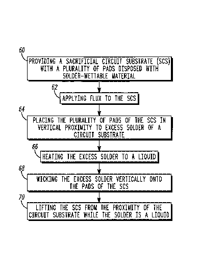
The present invention also encompasses a method for vertical removal of
excess solder from a circuit substrate. Refernng to FIG. 6, the method
includes a first
step 60 of providing a sacrificial circuit substrate with a plurality of pads
and
optionally vias. Preferably, the circuit substrate is a flexible circuit board
and the
sacrificial circuit substrate is a rigid circuit board. However, the
sacrificial circuit
substrate can also be flexible or rigid. A portion of each pad and via has a
solder-
wettable material disposed thereon. In particular, this step 60 includes
providing the
pads connected to the vias with through-holes that are plated with a solder-
wettable
material.
CA 02541977 2006-04-06
WO 2005/044499 PCT/US2004/027339
Preferably, a next step 62 includes applying flux to the sacrificial circuit
substrate, or to the site to be reworked.
A next step 64 includes placing the plurality of pads and vies of the
sacrificial
circuit substrate in vertical proximity to the excess solder of the circuit
substrate.
A next step 66 includes heating the excess solder to a liquidous state.
Preferably, includes using hot air or other hot gas such as nitrogen to reflow
the
excess solder. A solder reflow temperature profile similar to one used for BGA
removal is run to cause the excess solder to become liquidous and to wet the
pads and
vies of the sacrificial circuit substrate.
10 A next step 68 includes wicking the excess solder vertically onto the pads
and
into the optional vies of the sacrificial circuit substrate. Preferably, this
step includes
applying a vacuum to the vies to assist wickingof the solder into the through-
holes of
the vies, but can be done without vacuum through capillary action of the
solder in the
vies.
A next step 70 includes vertically lifting the sacrificial circuit substrate
from
the proximity of the circuit substrate while the solder is in a liquidous
state. The
vacuum from the previous step 68 can be used for this purpose. For example,
while
the solder is in a liquid state, the sacrificial circuit substrate is lifted
using the vacuum
function. The lifting is done vertically to prevent damage to the solder mask
of the
circuit substrate. In practice, the dimensions of the pads, vies and through-
holes of
the providing step 60 are configured to leave.a desired residual amount of
solder on
the circuit substrate after the wicking 68 and lifting 70 steps.
The above description of the present invention is intended to be exemplary
only and is not intended to limit the scope of any patent issuing from this
application.
CA 02541977 2006-04-06
WO 2005/044499 PCT/US2004/027339
11
The present invention is intended to be limited only by the broad scope of the
following claims.