Note : Les descriptions sont présentées dans la langue officielle dans laquelle elles ont été soumises.
CA 02543516 2006-04-13
BALLAST WITH OUTPUT GROUND-FAULT PROTECTION
Field of the Invention
The present invention relates to the general subject of circuits for
powering discharge lamps. More particularly, the present invention relates to
a
ballast that includes circuitry for protecting the ballast in the event of an
output
ground-fault.
Background of the Invention
A number of existing electronic ballasts have non-isolated outputs. Such
ballasts typically include circuitry for protecting the ballast inverter from
damage
in the event of a lamp fault condition (e.g., removal or failure of a lamp).
Occasionally, the output wiring of a ballast (i.e., the wires that connect
the ballast to the lamp(s)] becomes shorted to earth ground via the lighting
fixture. Such a condition can arise, for example, due to the output wires
becoming loose or pinched. For ballasts with non-isolated outputs, if the
inverter begins to operate while an earth ground short is present at one or
more
of the output wires, a large low frequency (e.g., 60 hertz) current may flow
through the inverter transistors and cause them to fail.
U.S. Patent 6,657,400 B2 (entitled "Ballast with Protection Circuit for
Preventing Inverter Startup During an Output Ground-Fault Condition" and
assigned to the same assignee as the present invention) discloses a ballast
that
includes an output ground-fault protection circuit. The ground-fault
protection
circuit that is disclosed in the 6,657,400 patent is well suited for many
ballasts,
but has the drawback of requiring additional discrete circuitry in order to
provide
output ground-fault protection.
In recent years, it has become increasingly common for electronic
ballasts to include a programmable microcontroller that coordinates and
controls
multiple functions (e.g., lamp fault protection) within the ballast. For such
ballasts, a need exists for a ground-fault protection approach that can be
realized
with little or no additional circuitry. A ballast that includes such a ground-
fault
protection approach would represent a significant advance over the prior art.
CA 02543516 2006-04-13
2
Brief Description of the Drawings
FIG. 1 is a block diagram schematic of a ballast with output ground-fault
protection, in accordance with the preferred embodiments of the present
invention.
FIG. 2 is a detailed electrical schematic of a ballast with output ground-
fault protection, in accordance with a first preferred embodiment of the
present
invention.
FIG. 3 is a detailed electrical schematic of a ballast with output ground-
fault protection, in accordance with a second preferred embodiment of the
present invention.
FIG. 4 is a flowchart that describes a method for protecting a ballast
from an output ground-fault condition, in accordance with the preferred
embodiments of the present invention.
CA 02543516 2006-04-13
Detailed Description of the Preferred Embodiments
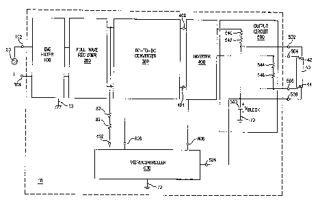
FIG. 1 describes a ballast 10 for powering at least one gas discharge lamp
40. Ballast 10 comprises an EMI filter 100, a full-wave rectifier 200, a DC-to-
DC converter 300, an inverter 400, an output circuit 500, and a
microcontroller
600.
EMI filter 100 includes input terminals 102,104 adapted to receive a
conventional source of alternating current (AC) voltage 50, such as 120 volts
rms at 60 hertz. Full-wave rectifier 200 is coupled to EMI filter 100. DC-to-
DC
converter 300 is coupled to full-wave rectifier 200. Inverter 400 is coupled
to
DC-to-DC converter 300. Output circuit 500 is coupled to inverter 400, and
includes output terminals 502,504,506,508 adapted for connection to gas
discharge lamp 40. Microcontroller 600 is coupled to DC-to-DC converter 300,
inverter 400, and output circuit 500.
During operation, DC-to-DC converter 300 receives a full-wave rectified
voltage from full-wave rectifier 200 and provides a substantially direct
current
(DC) output voltage to inverter 400 via terminals 402,404. DC-to-DC converter
300 has a non-operating mode (during which the DC output voltage is
substantially zero, which occurs prior to startup of the DC-to-DC converter)
and
an operating mode (during which the DC output voltage is substantially greater
than zero, which occurs after startup of the DC-to-DC converter). In response
to
an output ground-fault condition wherein at least one of output terminals
502,504,506,508 is shorted to earth ground, microcontroller 600 directs DC-to-
DC converter 300 to remain in the non-operating mode. By forcing DC-to-DC
converter 300 to remain in the non-operating mode if an output ground-fault
condition is present, microcontroller 600 protects inverter 400 from damage
that
would otherwise occur. Preferably, microcontroller 600 is realized by an
integrated circuit (IC), such as a ST7LITE1B microcontroller IC manufactured
by ST Microelectronics, along with associated peripheral circuitry.
Turning now to FIG. 2, in a first preferred embodiment of the present
invention, ballast 20 includes a DC-to-DC converter 300 that is implemented as
a Sepic converter. Sepic converter 300 comprises a first inductor 310, an
electronic switch 320 (preferably implemented as a N-channel field effect
CA 02543516 2006-04-13
4
transistor), a first capacitor 325, a drive circuit 330, a second inductor
340, a
diode 350, and a second capacitor 360. Further details regarding the
construction and theory of operation of Sepic converter 300 are well known to
those skilled in the art of power supplies and electronic ballasts, and thus
will
not be further elaborated upon herein. Nevertheless, for purposes of
understanding the present invention, it is important to appreciate that, while
in
the non-operating mode (i.e., during which time drive circuit 325 does not
commutate electronic switch 320), the output voltage (provided between
terminals 402,404) of Sepic converter 300 is approximately zero. When an
output ground-fault condition is detected following application of power to
ballast 20, microcontroller 600 directs Sepic converter 300 to remain in the
non-
operating mode, thereby ensuring that substantially zero voltage is supplied
to
inverter 400. This protects inverter 400 from the damage that would otherwise
occur due to presence of a ground-fault at any of output terminals
502,504,506,508.
As described in FIG. 2, EMI filter 100 includes magnetically coupled
inductors 120,122, an X-capacitor 130, and a Y-capacitor 140 having one end
that is coupled to earth ground 60. Full-wave rectifier 200 includes a diode
bridge 210 and a capacitor 220. Inverter 400 is preferably implemented as a
half bridge type inverter that includes first and second inverter switches
410,420
(preferably realized by N-channel field-effect transistors) and an inverter
drive
circuit 430 that provides substantially complementary commutation of inverter
switches 410,420. Output circuit 500 is preferably implemented as a series
resonant type output circuit comprising first, second, third, and fourth
output
terminals 502,504,506,508, a resonant inductor 510, a resonant capacitor 520,
a
direct current (DC) blocking capacitor 530, a first filament heating circuit
comprising a first winding 512 (preferably, first winding 512 is magnetically
coupled to resonant inductor 510) and a first capacitor 522, a second filament
heating circuit comprising a second winding 514 (preferably, second winding
514 is magnetically coupled to resonant inductor 510) and a second capacitor
524, and filament path resistors 540,542,544,546. First and second output
terminals 502,504 are adapted for connection to a first filament 42 of lamp
40.
CA 02543516 2006-04-13
Third and fourth output terminals 506,508 are adapted for connection to a
second filament of lamp 40. DC blocking capacitor 530 is coupled between
fourth output terminal 508 and circuit ground 70.
As known to those skilled in the art of power supplies and electronic
5 ballasts, output circuit 500 may be modified in certain well-known ways
(which
differ from that which is described in FIG. 2) without substantially affecting
the
desired operation of ballast 20. For example, the lower end of resonant
capacitor
520 may alternatively be coupled directly to circuit ground 70 (instead of
being
coupled to fourth output terminal 508 and the top of DC blocking capacitor
530).
As a further example, capacitors 522,524 in the first and second filament
heating
circuits may be replaced with diodes. Various other modifications to output
circuit 500 will be apparent to those skilled in the art of power supplies and
electronic ballasts.
Referring again to FIG. 2, microcontroller 600 includes a startup input
602, a detection input 604, a first control output 606, and a second control
output
608. It should be appreciated that, in an actual ballast, microcontroller 600
will
include additional inputs and outputs (for the sake of clarity, those inputs
and
outputs are not shown or described herein) for implementing other ballast
control functions, such as lamp fault protection, control of lamp current or
power, and so forth. As described in FIG. 2, startup input 602 is coupled to
the
output of full-wave rectifier 200 via resistors 80,82. During operation,
startup
input 602 receives voltage/current necessary for operating microcontroller
600.
Detection input 604 is coupled to DC blocking capacitor 530 and fourth output
terminal 508. During operation, detection input 604 allows microcontroller 600
to monitor a voltage, VBLOCK, across DC blocking capacitor 530. The magnitude
of VBLOCK prior to startup of Sepic converter 300 indicates whether or not an
output ground-fault condition is present. More specifically, if a voltage that
is
greater than a predetermined threshold value (e.g., 100 millivolts) is present
at
detection input 604 prior to startup of Sepic converter 300, then an output
ground-fault condition is deemed to be present; in response, microcontroller
600
directs Sepic converter 300 to remain in the non-operating mode. In this way,
microcontroller protects inverter 400 from being damaged when an output
CA 02543516 2006-04-13
6
ground-fault is present. Conversely, if a voltage that is less than the
predetermined threshold value (e.g., 100 millivolts) is present at detection
input
604 throughout the period prior to startup of Sepic converter 300, then an
output
ground-fault condition is deemed to not be present; in response,
microcontroller
600 allows Sepic converter 300 to enter the operating mode.
For practical reasons, it is preferred that the predetermined threshold
value be a small nonzero voltage that is on the order of about 100 millivolts
or
so. This is desirable in order to provide some degree of immunity to possible
electrical noise (that might otherwise falsely indicate an output ground-fault
condition).
The detailed operation of ballast 20 is now explained with reference to
FIG. 2 as follows.
During normal operation, when no output ground-fault is present, ballast
operates in the following manner. When power is initially applied to ballast
15 20 (at t = 0), DC-to-DC converter 300, inverter 400, and microcontroller
600 are
initially off. Within a short period of time following initial application of
power
to ballast 20, microcontroller 600 turns on due to the voltage provided to
startup
input 602. At that point, DC-to-DC converter 300 and inverter 400 are still
off.
DC-to-DC converter 300 will remain off (i.e., in the non-operating mode) for a
20 predetermined startup delay period (i.e., 0 < t < t,). With microcontroller
600
turned on, microcontroller 600 monitors (via detection input 604) the voltage,
VsLOCK~ across DC blocking capacitor 530. Because no output ground-fault is
present, and because both DC-to-DC converter 300 and inverter 400 are not yet
operating, VBLOCK will be approximately zero during this time. Accordingly, at
the end of the predetermined startup delay period (i.e., t = t~),
microcontroller
600 will allow DC-to-DC converter 300 to start in a normal manner, at which
point DC-to-DC converter 300 will provide a nonzero output voltage between
terminals 402,404. Inverter 400 subsequently starts and proceeds to provide,
via
output circuit 500, voltages for preheating lamp filaments 42,44, a high
voltage
for igniting lamp 40, and a magnitude-limited current for operating lamp 40
after
ignition.
CA 02543516 2006-04-13
7
If, on the other hand, an output ground-fault condition is present (i.e., at
least one of output terminals 502,504,506,508 is shorted to earth ground),
ballast
20 operates in the following manner. When power is initially applied to
ballast
20 (at t = 0), DC-to-DC converter 300, inverter 400, and microcontroller 600
are
initially off. Within a short period of time following initial application of
power
to ballast 20, microcontroller 600 turns on due to the voltage provided to
startup
input 602. At that point, DC-to-DC converter 300 and inverter 400 are still
off.
DC-to-DC converter 300 will remain off (i.e., in the non-operating mode) for a
predetermined startup delay period (i.e., 0 < t < tl). With microcontroller
600
turned on, microcontroller 600 monitors (via detection input 604) the voltage,
VBLOCK~ across DC blocking capacitor 530. With an output ground-fault
condition present, a low frequency (e.g., 60 hertz) current flows up from
earth
ground 60 to the shorted output terminal (502 or 504 or 506 or 508), through
one
or both lamp filaments 42,44 (depending on which output terminal is shorted to
earth ground), through filament path resistors 544,546 (if the ground-fault is
present at output terminal 502 or 504), through DC blocking capacitor 530, and
into circuit ground 70. The resulting low frequency current that flows in the
event of an output ground-fault causes a nonzero voltage that is substantially
greater than a predetermined threshold value (e.g., 100 millivolts) to develop
across DC blocking capacitor 70. That nonzero voltage is detected by
microcontroller 600, which responds by directing Sepic converter 300 to remain
off (i.e., in the non-operating mode). In this way, ballast 20 is protected
from the
damage (e.g., destruction of inverter transistors 410,420) that would
otherwise
occur due to an output ground-fault condition.
As described herein, microcontroller 600 is responsive to protect ballast
20 from a ground-fault condition at either of output terminals
502,504,506,508.
However, it should be appreciated that, in the absence of appropriate
protection,
a ground-fault at output terminal 502 or 504 would be potentially more
destructive than a ground-fault at output terminal 506 or 508.
Turning now to FIG. 3, in a second preferred embodiment of the present
invention, ballast 30 includes a DC-to-DC converter that is implemented as a
buck converter 300'. Buck converter 300' comprises an inductor 310, an
CA 02543516 2006-04-13
8
electronic switch 320 (preferably realized by a N-channel field-effect
transistor),
a drive circuit 330', a diode 350, and a capacitor 360. Details regarding the
construction and theory of operation of buck converter 300' are well known to
those skilled in the art of power supplies and electronic ballasts, and thus
will
not be further elaborated upon herein. However, for purposes of understanding
the present invention, it is important to appreciate that, while in the non-
operating mode (i.e., during which time drive circuit 325' does not commutate
electronic switch 320), the output voltage (provided between terminals
402,404)
of buck converter 300' is approximately zero. When an output ground-fault
condition is detected following application of power to ballast 20,
microcontroller 600 directs buck converter 300 to remain in the non-operating
mode, thereby ensuring that substantially zero voltage is supplied to inverter
400. This protects inverter 400 from the damage that would otherwise occur due
to the presence of a ground-fault at any of output terminals 502,504,506,508.
In the second preferred embodiment, as described in FIG. 3, the preferred
structures for EMI filter 100, full-wave rectifier 200, inverter 400, output
circuit
500, and microcontroller 600 are identical to that which was previously
described in connection with the first preferred embodiment (i.e., ballast 20)
described in FIG. 2. Moreover, the detailed operation of ballast 30 is
essentially
the same as that which was previously described with reference to ballast 20
(FIG. 2).
FIG. 4 describes a method, for a ballast that includes a DC-to-DC
converter and a direct current (DC) blocking capacitor, for protecting the
ballast
from an output ground-fault condition. The method 700 comprises the steps of:
(1) applying power to the ballast (step 710); (2) activating a microcontroller
(step 720); (3) providing a startup delay period (0 < t < t1) for the DC-to-DC
converter (step 730); (4) monitoring a voltage, VBLOCK~ across the direct
current
(DC) blocking capacitor during the startup delay period (step 740); (4) in
response to VBLOCK being greater than a predetermined threshold value (e.g.,
100
millivolts) during the startup delay period, preventing startup of the DC-to-
DC
converter (decision block 742 and step 750); (5) in response to VBLOCK being
less than the predetermined threshold value throughout the startup delay
period,
CA 02543516 2006-04-13
9
allowing startup of the DC-to-DC converter at t = t~ (decision blocks 742,744
and step 760). In accordance with the first and second preferred embodiments
described herein, the steps of monitoring (step 740), preventing (step 750),
and
allowing (step 760) are executed via the microcontroller, and the DC-to-DC
converter is preferably implemented as either a Sepic converter or a buck
converter. Moreover, it is preferred that the predetermined threshold value be
a
small nonzero voltage that is on the order of about 100 millivolts or so, in
order
to provide some degree of immunity to electrical noise.
Although the present invention has been described with reference to
certain preferred embodiments, numerous modifications and variations can be
made by those skilled in the art without departing from the novel spirit and
scope of this invention. For example, although the present description of the
preferred embodiment has been directed to ballasts 10,20,30 that power a
single
gas discharge lamp 40, it should be appreciated that the principles of the
present
invention are readily extended and applied to ballasts that power multiple gas
discharge lamps. Additionally, the DC-to-DC converter is not limited to a
Sepic
or buck converter, but may be implemented by any other type of converter
(e.g.,
a flyback converter or a buck+boost converter) that provides a substantially
zero
output voltage prior to startup.
What is claimed is: