Note : Les descriptions sont présentées dans la langue officielle dans laquelle elles ont été soumises.
CA 02544166 2006-04-28
WO 2005/044571 PCT/US2004/034795
1
INTERCONNECT CIRCUIT
Background
An inkjet printer forms a printed image by printing a pattern of individual
dots at particular locations of an array defined for the printing medium. The
locations may be visualized as being small dots in a rectilinear array. The
locations are sometimes called "dot locations," "dot positions," or "pixels."
Thus,
a printing operation can be viewed as providing a pattern of dot locations
with
dots of ink.
Inkjet printers print pixels by ejecting drops of ink from ink ejecting
nozzles onto the print medium and typically include a movable print carriage
that
supports one or more print cartridges. The print carriage traverses axially
above
the surface of the print medium, while the nozzles are controlled to eject
drops
of ink at appropriate times pursuant to command of a microcomputer or other
controller. The timing of the application of the ink drops is intended to
correspond to the pattern of pixels of the image being printed.
The particular ink ejection mechanism within the printhead may take on a
variety of different forms known to those skilled in the art, such as those
using
thermal ejection or piezoelectric technology. For instance, two exemplary
thermal ejection mechanisms are shown in commonly assigned U.S. Patent
Nos. 5,278,584 and 4,683,481. In a thermal ejection system, an ink barrier
layer containing ink channels and ink vaporization chambers is disposed
between a nozzle orifice plate and a thin film substrate. The thin film
substrate
typically includes arrays of heater elements such as thin film resistors which
are
selectively energized to heat ink within the vaporization chambers. When the
heater elements are energized, an ink droplet is ejected from a nozzle
associated with the heater element. By selectively energizing heater elements,
CA 02544166 2006-04-28
WO 2005/044571 PCT/US2004/034795
2
ink drops are ejected onto the print medium in a pattern to form the desired
image.
Certain inkjet printers employ replaceable print cartridges. The print
cartridges and printers employ electrical interconnects between the cartridge
and the printer, so that operation of the print cartridge can be controlled by
the
printer. The electrical interconnects can be in the form of an interconnect
array
having a plurality of discrete interconnect pads. The use of replaceable print
cartridges in inkjet printers allows the possibility that a user may install
or
attempt to install a replacement print cartridge that is not designed for use
with
the user's particular printer or with the particular chute of the particular
printer.
The incorrect installation of a print cartridge in a printer can result in
dangerous
situations where electrical circuits are energized incorrectly, causing damage
to
the print cartridge, the printer, or both. This damage may cause substantially
loss for users. Therefore, consideration must be given to the prevention of
use
of a print cartridge that will not operate properly in the chute or printer.
One solution to prevent incorrect use of a print cartridge in a printer is to
make each print cartridge with a physically different shape from other print
cartridges for other printers or chutes, so that there is no possibility of a
printer
accepting an incorrect cartridge. This solution requires very different
production
lines for print cartridges and printers and is consequently costly to
implement.
Another solution is to have similar print cartridges, but provide unique
physical
keys on the cartridge and printer so that an incorrect cartridge cannot be
inserted into a printer. This solution can be defeated by a user who removes
or
modifies the physical keys. Yet another solution is to have physically similar
print cartridges, and to make sure that the positions of the interconnect pads
do
not overlap between cartridges intended for different printers or different
chutes.
This solution becomes unreasonably difficult to implement, as eventually
interconnect pad positions will overlap as the number of interconnect pads
increases (increasing performance) and/or the size of the interconnect array
decreases (decreasing cost).
CA 02544166 2008-11-05
3
Summary
According to one aspect of the present invention there is provided a fluid
ejection device that is part of a predetermined set of fluid ejection devices
comprising a body having a lower portion and a vertical wall, a printhead
coupled
with the lower portion and a contact array comprising a plurality of contact
areas
disposed on the vertical wall. The contact array is one of a predetermined set
of
contact arrays comprising a first contact array having a first layout of
contact
area locations, and a second contact array having a second layout of contact
area locations. A portion of the contact area locations on the first layout
are
different from a portion of contact area locations of the second layout.
Another
portion of the contact area locations of the first layout and another portion
of
contact area location of the second layout are the same. The another portion
of
contact area locations of the first layout and the another portion of the
contact
area locations of the second layout are coupled to provide identification
information for the fluid ejection device.
Brief Description of the Drawings
Figure 1 is a block diagram illustrating one embodiment of an inkjet
printing system.
Figure 2 is a schematic perspective view of an embodiment of an inkjet
print cartridge.
Figure 3 is a schematic side elevational view of the embodiment of the
inkjet print cartridge of Figure 2.
Figure 4 is a schematic bottom plan view of the embodiment of the inkjet
print cartridge of Figure 2.
Figure 5A is a schematic detail view of an embodiment of a flexible circuit
of the inkjet print cartridge of Figure 2.
Figure 5B is a schematic detail view of another embodiment of a flexible
circuit of the inkjet print cartridge of Figure 2.
Figure 6 is a schematic detail view of yet another embodiment of a
flexible circuit of the inkjet print cartridge of Figure 2.
Figure 7 is a schematic perspective view of an embodiment of a print
carriage used in the mounting assembly of Figure 1.
Figure 8 is a schematic front elevational view of an embodiment of a
chute and latch of the print carriage of Figure 7.
Figure 9 is a schematic partial front perspective view of the embodiment
of the print carriage of Figure 7, with the cartridges and the latch
assemblies
removed.
CA 02544166 2006-04-28
WO 2005/044571 PCT/US2004/034795
4
Figure 10 is a schematic sectional elevational view of the embodiment of
a chute and latch assembly of the print carriage of Figure 7.
Figure 11 is a schematic sectional elevational view of the embodiment of
a chute of the print cartridge of Figure 7.
Figure 12 is a flowchart of an embodiment of a method for detecting an
incorrect print cartridge according to the invention.
Figure 13 is a flowchart of an embodiment of the method of Figure 12,
using the flexible circuit implementations of Figures 5A and 6.
Detailed Description
In the following Detailed Description, reference is made to the
accompanying drawings which form a part hereof, and in which is shown by way
of illustration particular embodiments in which the invention may be
practiced.
In this regard, directional terminology, such as "top," "bottom," "front,"
"back,"
"leading," "trailing," etc., is used with reference to the orientation of the
Figure(s)
being described. Because components of embodiments of the present
invention can be positioned in a number of different orientations, the
directional
terminology is used for purposes of illustration and is in no way limiting. It
is to
be understood that other embodiments may be utilized and structural or logical
changes may be made without departing from the scope of the present
invention. The following detailed description, therefore, is not to be taken
in a
limiting sense, and the scope of the present invention is defined by the
appended claims.
FIG. 1 illustrates one embodiment of an inkjet printing system 10. Inkjet
printing system 10 includes an inkjet printhead assembly 12 and an ink supply
assembly 14. In the illustrated embodiment, inkjet printing system 10 also
includes a mounting assembly 16, a media transport assembly 18, and an
electronic controller 20.
Inkjet printhead assembly 12 includes one or more print heads which
eject drops of ink or fluid through a plurality of orifices or nozzles 13. In
one
embodiment, the drops are directed toward a medium, such as print medium 19,
so as to print onto print medium 19. Print medium 19 may be any type of
CA 02544166 2006-04-28
WO 2005/044571 PCT/US2004/034795
suitable sheet material, such as paper, card stock, transparencies, Mylar,
fabric,
and the like. Typically, nozzles 13 are arranged in one or more columns or
arrays such that properly sequenced ejection of ink from nozzles 13 causes, in
one embodiment, characters, symbols, and/or other graphics or images to be
5 printed upon print medium 19 as inkjet printhead assembly 12 and print
medium
19 are moved relative to each other.
Ink supply assembly 14 supplies ink to printhead assembly 12 and
includes a reservoir 15 for storing ink. As such, in one embodiment, ink flows
from reservoir 15 to inkjet printhead assembly 12. In one embodiment, inkjet
printhead assembly 12 and ink supply assembly 14 are housed together in an
inkjet or fluid jet cartridge or pen, also referred to as a print cartridge.
In another
embodiment, ink supply assembly 14 is separate from inkjet printhead assembly
12 and supplies ink to inkjet printhead assembly 12 through an interface
connection, such as a supply tube (not shown).
Mounting assembly 16 positions inkjet printhead assembly 12 relative to
media transport assembly 18, and media transport assembly 18 positions print
medium 19 relative to inkjet printhead assembly 12. In one embodiment, inkjet
printhead assembly 12 is a scanning type printhead assembly and mounting
assembly 16 includes a carriage (not shown) for moving inkjet printhead
assembly 12 relative to media transport assembly 18. In another embodiment,
inkjet printhead assembly 12 is a non-scanning type printhead assembly, e.g. a
page wide printhead assembly, and mounting assembly 16 fixes inkjet printhead
assembly 12 at a prescribed position relative to media transport assembly 18.
Electronic controller 20 communicates with inkjet printhead assembly 12,
mounting assembly 16, and media transport assembly 18. Electronic controller
20 receives data 21 from a host system, such as a computer, and usually
includes memory for temporarily storing data 21. Typically, data 21 is sent to
inkjet printing system 10 along an electronic, infrared, optical or other
information transfer path. Data 21 represents, for example, a document and/or
file to be printed. As such, data 21 forms a print job for inkjet printing
system 10
and includes one or more print job commands and/or command parameters.
CA 02544166 2006-04-28
WO 2005/044571 PCT/US2004/034795
6
In one embodiment, electronic controller 20 provides control of inkjet
printhead assembly 12 including timing control for ejection of ink drops from
nozzles 13. As such, electronic controller 20 defines a pattern of ejected ink
drops which form characters, symbols, and/or other graphics or images on print
medium 19. Timing control and, therefore, the pattern of ejected ink drops is
determined by the print,job commands and/or command parameters. In one
embodiment, at least a portion of logic and drive circuitry forming a portion
of
electronic controller 20 is located on inkjet printhead assembly 12. In
another
embodiment, at least a portion of logic and drive circuitry is located off
inkjet
printhead assembly 12.
Inkjet printing system 10 of FIG. 1 constitutes one embodiment of a fluid
ejection system which includes a fluid ejection device. In other embodiments,
inkjet printing system 10 can be a fluid ejection system that ejects any
desired
liquid onto a desired surface. Embodiments of fluid ejection devices used in
fluid ejection systems include, but are not limited to, inkjet printheads,
inkjet print
cartridges or pens, fluid jet print cartridges or pens, fluid ejecting
integrated
circuits, and fluid ejecting nozzles.
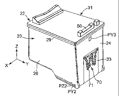
FIGS. 2-4 illustrate one embodiment of a print cartridge 22. The print
cartridge 22 includes a housing 23 that supports inkjet printhead assembly 12
and contains reservoir 15 of ink supply 14. As such, reservoir 15 communicates
with inkjet printhead assembly 12 to supply ink to inkjet printhead assembly
12,
as is well known in the art. Housing 23 is comprised of a rear wall 24, a left
side
wall 25, a right side wall 26, a front wall 27, and a bottom wall 28 that
includes a
snout section 28a that supports an inkjet printhead assembly 12. A top wall or
lid 31 is attached to the upper edges of the front, side, and rear walls, and
includes margins or lips 29 that extend beyond the front and side walls. A
latch
catch or feature 50 is disposed on the lid 31 close to the top boundary of the
rear wall 24. The latch feature 50 extends upwardly from the top wall 31.
Other shapes may be utilized for housing 23, including, but not limited to,
cubic, triangular, etc. Further, snout section 28a and lips 29 may be omitted
depending on the design parameters.
CA 02544166 2006-04-28
WO 2005/044571 PCT/US2004/034795
7
Located in the vicinity of the intersection of the left side wall 25, rear
wall
24 and snout 28a are a printhead cartridge X axis datum PX1, a first printhead
cartridge Y axis datum PY1, and a first printhead cartridge Z axis datum PZ1.
Located in the vicinity of the intersection of the right side wall 26, rear
wall 24
and snout 28a are a second printhead cartridge Y axis datum PY2 and a
second printhead cartridge Z axis datum PZ2. A third printhead cartridge Y
axis
datum PY3 is located in the upper portion of the rear wall 24. The print
cartridge
Y axis datums generally comprise lands that are configured to be generally
orthogonal to the Y axis when the cartridge is installed in the mounting
assembly 16. The print cartridge Z axis datums comprise lands that are
configured to be generally orthogonal to the Z axis when the print cartridge
is
installed in the mounting assembly 16. The print cartridge X axis datum
comprises land that is configured to be generally orthogonal to the X axis
when
the print cartridge is installed in the mounting assembly 16. As described
further
herein, the datums of the cartridge engage corresponding datums in the
mounting assembly 16.
Other numbers, locations and combinations of datums may be utilized on
cartridge 22, or datums may be omitted entirely, depending on the design
parameters.
Disposed on the rear wall 24, but which can be located on one of the
other walls depending on design parameters, is an electrical circuit 33 that
provides electrical interconnection between the printer and the printhead 15.
Electrical circuit 33 facilitates communication of electrical signals between
electronic controller 20 and inkjet printhead assembly 12 for controlling
and/or
monitoring operation of inkjet printhead assembly 12. Electrical circuit 33
includes an array 70 of electrical contact areas 71 and a plurality of
conductive
paths 77 (best seen in FIGS. 5A and 6) that extend between and provide
electrical connection between electrical contact areas 71 and bond pads 74 on
the inkjet printhead assembly 12. As such, electrical contact areas 71 provide
points for electrical connection with printing cartridge 22 and, more
specifically,
inkjet printhead assembly 12. In one embodiment according to the invention,
electrical circuit 33 is a flexible electrical circuit, and conductive paths
77 are
CA 02544166 2006-04-28
WO 2005/044571 PCT/US2004/034795
8
formed in one or more layers of a flexible base material. The base material
may
include, for example, a polyimide or other flexible polymer material (e.g.,
polyester, poly-methyl-methacrylate) and conductive paths 77 may be formed of
copper, gold, or any other conductive material
FIG. 5A is a schematic depiction of an embodiment of the flexible circuit
33. Contact areas 71 are contactively engagable from the near side of the
flexible circuit 33 which is the side that is away from the cartridge body.
The
side of the flexible circuit 33 that is against the cartridge body is called
the far
side. The contact areas 71 are disposed on a portion of the flexible circuit
33
that is located on the rear wall 24, and comprise electrically conductive
areas
that are contactively engageable with corresponding contact bumps 139 on a
resilient contact circuit 137 (FIG. 9) located in the mounting assembly 16
(FIG.
1). In the embodiment depicted in FIG. 5A, the flexible circuit 33 is formed
of a
flexible substrate on one side thereof and includes openings so that portions
of
the conductive pattern can be contacted from the other side of flexible
circuit 33.
In such implementation, the contact areas 71 comprise conductive areas
exposed by openings in the flexible substrate. The contact areas 71 can be
circular, octagonal, square, square with rounded or beveled corners, or any
other shape or geometry.
In the exemplary embodiment of FIG. 5A, the contact areas 71 are more
particularly arranged in a plurality of adjacent, transversely separated
columnar
arrays 73 of contact areas 71. Each columnar array 73 includes a lower contact
area 71' that is closest to the bottom wall 28 of the print cartridge 22. By
way of
illustrative example, one or more of the columnar arrays 73 can be
substantially
nonlinear. The substantially nonlinear arrangement of contact areas 71 within
columnar arrays 73 allows the positioning of contact areas 71 to provide space
where it is needed for conductive paths 77 to pass by where space is limited.
The columnar arrays 73 are arranged in side by side pairs or groups 75a, 75b
of
columnar arrays 73. As shown in FIG. 5A, there can be two pairs 75a, 75b of
columnar arrays 73 so as to have four columnar arrays 73 of contact areas 71.
The columnar arrays 73 of each pair 75a, 75b are arranged to converge toward
each other in the direction toward the bottom wall 28 of the cartridge 22.
CA 02544166 2006-04-28
WO 2005/044571 PCT/US2004/034795
9
The contact array 70 further includes a horizontal row 76 of contact areas
71 substantially perpendicular to the columnar arrays 73. Row 76 is positioned
adjacent the top of contact array 70. The horizontal row 76 makes efficient
use
of space within contact array 70, thereby reducing the number of required
columnar arrays 73 and allowing the array 70 to be narrower. Other array
shapes and structure different that those depicted herein may be utilized in
the
present embodiments.
The outermost transversely separated columnar arrays designated 73'
can have more contact areas 71 than the columnar arrays 73 between such
outermost transversely separated columnar arrays 73'. By way of example,
each outermost columnar array 73' may include at least seven contact areas 71,
and each of the other columnar arrays 73 may include at least six contact
areas
71. Additionally, the outermost transversely separated columnar arrays 73' may
have fewer or the same number of contact areas 71 as columnar arrays 73.
The spacing between contact areas 71 is asymmetric, which allows a
reduction of the size of array 70, as compared to symmetric spacing. When the
cartridge 22 is used in a printer, the flexible circuit 33 of cartridge 22
mates with
resilient contact circuit 137 (FIG. 9) of the printer. The resilient contact
circuit
137 has design constraints for spacing between contact bumps 139, as well as
spacing between contact bumps 139 and conductive paths. The resilient
contact circuit 137 may route the conductive paths (not shown) away from the
contact bump 139 array in the opposite direction from the direction that the
conductive paths 77 are routed. Many of the conductive paths on both flexible
circuit 33 and resilient contact circuit 137 are routed between contact areas
71
and contact bumps 139, respectively. In instances where this is done, the
contact areas 71 and contact bumps 139 may be spaced farther apart from
each other. However, when there is not a conductive path between adjacent
contact areas 71 or adjacent contact bumps 139, the contact areas 71 and
contact bumps 139 can be spaced closer together. By utilizing asymmetric pad
spacing, columnar arrays 73 can be shorter than a columnar array with
symmetric spacing, since space is not wasted when conductive paths are not
CA 02544166 2006-04-28
WO 2005/044571 PCT/US2004/034795
routed between contact areas 71 on flexible circuit 33, or between contact
bumps 139 on the resilient contact circuit 137 of the printer.
In one embodiment according to the invention, where nonlinear arrays
73, asymmetric spacing of contact areas 71, and horizontal row 76 of contact
5 areas 71 are utilized, as illustrated in FIGS. 5A and 5B , the overall array
70
area is approximately 13.7 mm x 11.3 mm. An equivalent array using linear,
evenly spaced contact areas 71, as illustrated in FIG. 6, measures about 13.7
mm x 12.2 mm. The approximately 1 mm reduction in the width W of the array
allows the flexible circuit 33 to be laid out in 3 pitches (4.75 mm per pitch)
of a
10 48 mm flexible circuit, as opposed to 4 pitches. This alone results in a
savings of
approximately 25% of the area for the array 70.
In the embodiment of FIGS. 5A and 513, less than one half of the contact
areas 71 are positioned in the lower half of the smallest rectangle R, and
columnar arrays 73 extend across at least one half of the height of the
smallest
rectangle R. By way of example, for the contact array 70 depicted in FIG. 5A,
the smallest rectangle R has a height in the range of about 13.7 mm and a
width
W in the range of about 11.3 mm. Specifically, the rectangle R has a width of
less than about 12 mm. The contact areas 71 of the columnar arrays 73 can be
spaced center to center from each other by distances of less than 1 mm, about
1 mm to 3 mm, and greater than 3 mm. Depending upon implementation, some
or all of the contact areas 71 may be electrically connected to the inkjet
printhead assembly 12 by the conductive traces generally indicated by the
reference designation 77. The conductive traces are preferably disposed on the
farside of the flexible circuit 33, which is the side against the cartridge
housing,
and lead to bond pads 74 on the inkjet printhead assembly 12 (FIGS. 5A and
5B).
In the exemplary embodiment of FIG. 5A, the contact areas 71 include
enable line contact areas E1-E6 configured to receive signals which enable
energizing of heater elements; data line contact areas D1-D8 configured to
receive signals which provide print data representative of an image to be
printed; fire line contact areas F1-F6 configured to receive timed energy
pulses
employed to heat ink to be ejected from heater elements; ground line contact
CA 02544166 2008-11-05
11
areas GD1-GD6; a control signal contact area C configured to receive a signal
for controlling the internal operation of the printhead; a temperature sense
resistor contact area TSR, a temperature sense resistor return contact area
TSR-RT, and an identification bit contact area ID.
In an illustrative embodiment, all of the ground contact areas GD1-GD6
are interconnected by ground traces 79 that are on the flexible circuit 33.
Such
ground traces 77 can more particularly be located close to the columnar arrays
73 so as to be only on the portion of the flexible circuit that is on the rear-
wall of
the print cartridge body.
FIG. 5B shows a contact array 70 similar to that in FIG. 5A, but wherein
two contact areas 71 labeled NC are not used.
FIG. 6 shows another flexible circuit 33 having a contact array 70 with a
different arrangement of contact areas 71 from that illustrated in FIGS. 5A
and
5B. The exemplary embodiment of FIG. 6 is described in detail in United States
Patent No. 6,604,814, commonly assigned or under a duty of common
assignment herewith.
In the exemplary embodiment of FIG. 6, contact areas 71 are arranged in
a plurality of side by side transversely separated columnar arrays 73 of
contact
areas 71. The columnar arrays 73 can be substantially linear. The six columnar
arrays 73 of FIG. 6 are arranged in three side by side pairs or groups of
columnar arrays. Each pair of columnar arrays includes two columnar arrays 73
that diverge from each other in the direction toward the bottom wall of the
cartridge. Each columnar array 73 spans at least 70% if the height H of the
smallest rectangle R that encloses the array of contact areas 71 and defines a
region occupied b the contact areas 71. By way of example, for the exemplary
embodiment of FIG. 6, the smallest rectangle R has a height H in the range of
about 10 to 14 millimeters and a width W in the range of about 15 to 18
millimeters. The height to width ratio can be in a range of about 0.6 to 0.9.
Contact areas 71 include primitive select contact areas P1-P16, address signal
contact areas A1-A13, enable signal contact areas E1-E2, a temperature sense
CA 02544166 2006-04-28
WO 2005/044571 PCT/US2004/034795
12
resistor contact area TSR, an identification bit contact area ID, and ground
line
contact areas TG1, TG2, BG1, and BG2.
Referring now to FIGS. 7-11, one embodiment of a portion of mounting
assembly 16 is illustrated. Mounting assembly 16 includes a print carriage 119
having a base 126 that supports the structure, and two bearings 128 located at
the ends of the base 126. Bearings 128 slidably support the print carriage 119
on slider rod 121. The print carriage 119 further includes two chutes 131 that
each receive, hold, and align an inkjet print cartridge 22. Both chutes 131
are
constructed and operate similarly. Each chute includes a rear wall 135 that
comprises, for example, a portion of the base 126, a left side wall 133 that
extends from the rear wall 135, and a right side wall 134 that extends from
the
rear wall 135 and is generally parallel to the left side wall 133.
It should be noted that other configurations and mechanical components
may be used or included as part of mounting assembly 16. The configuration
and mechanical components of mounting assembly 16 as described herein are
designed for the embodiment of the fluid ejecting device illustrated in FIGS.
2-4.
However, the configuration and mechanical components of mounting assembly
16 will vary according to the design of both the fluid ejection system and the
fluid ejection device used therewith.
Carriage datums CY1, CZ1 and CX1, formed for example as part of the
base 126, are located at the bottom of the chute 131 in the vicinity of the
intersection of the left side wall 133 the rear wall 135, while carriage
datums
CY2 and CZ2 for example as part of the base 126 are located at the bottom of
the chute 131 in the vicinity of the intersection of the right side wall 134
and the
rear wall 135. A carriage datum CY3 is located on the rear wall 135.
A resilient contact circuit 137 is located on the rear wall 135 of the chute
and contains electrical contact bumps 139 that are urged against corresponding
contact areas 71 on the flex circuit 33 of the print cartridge 22. The contact
bumps 139 are arranged in a pattern having a mirror image of the pattern of
contact areas 71 of a print cartridge 22 intended for use with the printer.
The
resilient contact circuit 137 further functions as a resilient element that
urges the
print cartridge PY1, PY2 against carriage datums CY1, CY2 when the print
CA 02544166 2006-04-28
WO 2005/044571 PCT/US2004/034795
13
cartridge 22 is installed. By way of illustrative example, the resilient
contact
circuit 137 comprises a flexible circuit and resilient pad located between the
flexible circuit and the rear wall 135.
Located in each side wall 133, 134 is shaped guide channel 140. The
guide channels 140 engage lips 29 of the lid 31 of the print cartridge 22, and
guide the cartridge at an appropriate elevation and pitch (or rotation) of the
cartridge about the X axis as the cartridge is inserted, so as to guide the
cartridge into the general vicinity of the carriage datums. By way of
illustrative
example, each guide channel comprise upper and lower rails 140a, 140b or a
recessed slot having appropriate sides.
Located at the top of each chute 131 is a hinged latch assembly 150
(FIG. 7 and FIG. 10) that includes a latch support arm 151 that is pivotally
attached by a hinge 153 to the top of the rear wall 135 so as to be rotatable
about a hinge axis that is parallel to the X-axis. Latch hooks 155 are
provided
for engaging latch tabs 157 disposed at the front of the side walls 133, 134.
A pivoting biased clamp lever 159 is pivotally attached to the lower side
of the latch arm 151 so as to be pivotable about an axis that is parallel to
the X
axis. The clamp lever 159 extends generally toward the chute rear wall 135
when the latch is closed. The clamp lever 159 is biased by a spring 163 to
pivot
away from the latch arm 151. A land 167 is disposed at the distal portion of
the
pivoting clamp 159 for pushing down on the top portion of the latch feature 50
of
the print cartridge 22.
The pivoting clamp lever 159 further includes a sliding clamp 173 slidably
located for movement generally orthogonally to the pivoting clamp hinge axis.
The sliding clamp 173 is biased by a spring 175 to slide along the pivoting
clamp lever 159 away. A sliding clamp land 177 is disposed at the distal end
of
the sliding clamp 173 adjacent the pivoting clamp land 167.
In one embodiment, the cartridge 22 is inserted generally horizontally into
the chute 131. The guide channels 140 control the elevation and the pitch
about the X axis of the cartridge 22 as it is inserted into the chute 131,
such that
print cartridge datums PY1, PY2 move over the corresponding carriage datums
CY1, CY2. The latch arm 151 is then pivoted downwardly which causes the
CA 02544166 2006-04-28
WO 2005/044571 PCT/US2004/034795
14
sliding clamp land 177 and the pivoting clamp land 167 to eventually engage
the
latch feature 50 on the top of the cartridge. Continued displacement of the
latch
arm 151 causes the sliding clamp 173 to resiliently push on the latch feature
50
generally along the Y axis, and further causes the pivoting clamp lever 159 to
push on the latch feature 50 generally along the Z axis. The push generally
along the Y axis is independent of the push generally along the Z axis. The
push along the Z axis causes the print cartridge datums PZ1, PZ2 to snugly
seat
against the carriage datums CZ1, CZ2. The push along the Y axis causes the
print cartridge to pivot about the X axis so that the print cartridge datum
PY3
snugly seats against the carriage datum CY3. The resilient contact circuit 137
is
located so as to cause the print cartridge datums PY1, PY2 to seat snugly
against the carriage datum CY1, CY2 when the print cartridge datums PZ1, PZ2
are engaged with the carriage datums CZ1, CZ2, and the print cartridge datum
PY3 is engaged with the carriage datum CY3.
Other methods and arrangements for inserting print cartridge 22 into
assembly 16 may be utilized, depending on the design of both parts. Further,
other designs of chutes may be utilized depending on design parameters of
print cartridge 22 or vice-versa.
Referring again to FIGS. 5A, 5B and 6, it can be seen that the arrays 70
of the exemplary embodiments and the contact areas 71 therein are different in
their layouts. Differences include but are not limited to the pattern formed
by
contact areas 71, the spacing between contact areas 71, the overall size of
the
arrays 70, the number of contact areas 71 within the array, the functions of
the
contact areas 71, and the location of specific contact areas 71 within the
array,
to name a few, either individually or in combination. There are also some
similarities between the contact arrays 70. Similarities include but are not
limited to the function of some contact areas 71 (for example, ground contact
areas, temperature sense resistor contact areas, and identification bit
contact
areas), and the position of some specific contact areas 71 within the array.
In
other alternate embodiments according to the invention, the various contact
areas 71 described with respect to the exemplary embodiments may be
CA 02544166 2006-04-28
WO 2005/044571 PCT/US2004/034795
arranged in different patterns, spacing, shapes, sizes, functions and numbers
than the exemplary illustrated embodiments.
Print cartridges of different families (intended for use in different
printers,
groups of printers, or different chutes within the same or different printers)
may
5 have similar or identical physical shapes (that is, the housings 23 may be
substantially the same shape) and therefore be capable of insertion into a
variety of different printers. However, print cartridges of different families
may
also have different layouts of contact areas 71 on flexible circuit 33. For
example, a print cartridge intended for use in a first chute may have a
contact
10 array 70 like that illustrated in FIG. 6, while a print cartridge intended
for use in a
second chute may have a contact array 70 like that illustrated in FIG. 5A. The
contact bumps 139 of each chute will be configured for complete and proper
electrical engagement with only print cartridges that are to be operated by
the
printer in the particular chute. The printer may therefore be capable of
15 determining if a correct print cartridge (that is, a print cartridge that
is to operate
in the particular chute) is installed prior to attempting to print, so that
damage to
the printer, print cartridge, or both, can be avoided.
For the controller 20 of the printer to distinguish whether a print cartridge,
which is operable in the particular chute, has been installed a continuity and
diagnostics test is conducted. In some embodiments, the continuity and
diagnostics test is performed using lower currents, voltages, and/or powers
than
those required for operation, e.g. energizing of the heater elements, of a
print
cartridge in the chute.,
The ability to perform continuity and diagnostics testing may be assured
by designating one or more selected contact areas 71, which are to be used for
continuity and diagnostic testing, to specific positions within array 70 for
all print
cartridges. In this manner, for any print cartridge inserted into any chute of
any
printer, one or more selected contact areas 71 of the print cartridge will be
in
electrical contact with a corresponding contact bump 139 of the printer,
regardless of the printer type. If the print cartridge is identified as being
operable
in the particular chute, printing can proceed. If the print cartridge is
identified as
not being operable in the particular chute, printing may be prohibited until
the
CA 02544166 2006-04-28
WO 2005/044571 PCT/US2004/034795
16
correct print cartridge is inserted into the printer. One method of
determining
whether the print cartridge inserted is identified as the correct print
cartridge
involves, continuity and diagnostic testing as described herein.
The contact arrays 70 of FIGS. 5A and 6 provide examples of contact
area 71 layouts that permit a printer to conduct continuity and diagnostics
testing of print cartridges. In examining the contact arrays of FIGS. 5A and
6, it
can be seen that several contact areas 71 are similarly positioned or located
within their respective array 70, such that when the arrays 70 are overlaid on
each other, the similarly positioned or located contact areas 71 are
superimposed. The contact areas 71 that are similarly positioned or located
within their respective array may be said to be commonly positioned or
located.
The contact areas 71 that are not commonly positioned or located may be said
to be uniquely positioned or located within their respective array 70. In the
illustrated example, the TSR contact area of FIG. 5A overlays the TSR contact
area of FIG. 6 (contact area position 200); the TSR-RT contact area of FIG. 5A
overlays a ground contact area of FIG. 6 (contact area position 202); a ground
contact area of FIG. 5A overlays a ground contact area of FIG. 6 (contact area
position 204); the ID contact area of FIG. 5A overlays no contact areas of
FIG. 6
(contact area position 206); and a ground contact area of FIG. 5A overlays the
ID contact area of FIG. 6 (contact area position 208). Thus, in the
illustrated
example, the contact areas 71 in contact area positions 200, 202, 204, 208 may
be said to be said to be commonly positioned or located. All other contact
areas
71 may be said to be uniquely positioned or located.
Using the exemplary contact arrays 70 of FIGS. 5A and 6 as an example,
a chute may be configured to operably print using a first print cartridge
having a
contact array 70 like that illustrated in FIG. 5A. The chute may also be
configured when to be inoperably when it receives a second print cartridge
having a contact array 70 like that illustrated in FIG. 6. The controller 20
of the
printer may be capable of detecting and rejecting a print cartridge having a
contact array 70 like that illustrated in FIG. 6. Using the contact array
layouts of
FIGS. 5A and 6, the exemplary printer is able to read a value on the thermal
sense resistor of an installed print cartridge of either type (because the TSR
CA 02544166 2006-04-28
WO 2005/044571 PCT/US2004/034795
17
contact area of FIG. 5A overlays the TSR contact area of FIG. 6 at contact
area
position 200). However, the exemplary printer is unable to read the ID bit of
a
print cartridge using a contact array like that of FIG. 6 (because the ID
contact
area of FIG. 5A overlays no contact areas of FIG. 6 at contact area position
206). Using this information, the exemplary printer knows that a print
cartridge
is installed (because otherwise it could not read the value of the thermal
sense
resistor), and it also knows that the cartridge is a cartridge that is not be
operated in the particular chute (because no ID bits are readable). This
information allows the exemplary printer to prevent operation of the print
cartridge, and thereby prevent potential damage to the printer and/or print
cartridge.
Other alignments and configurations of one or more particular contact
bumps and contact areas may be used to identify specific print cartridge than
those described above.
Referring to the flowchart of FIG. 12, the printer controller 20 first
attempts to determine whether a print cartridge is installed in the chute (box
300). If no print cartridge is detected, printing operations end (box 302). If
controller 20 determines that a print cartridge is installed in the chute of
the
printer, the controller 20 attempts to determine if the installed print
cartridge is to
be operated from the chute into which it was installed (box 304). If a
cartridge is
not to be operated from the chute in which the cartridge is installed, then
the
printer is prevented from printing (box 302). If the cartridge is to be
operated
from the chute in which the cartridge is installed, then the printer is
allowed to
print (box 306).
Referring to the flowchart of FIG. 13, the method of FIG. 12 is illustrated
using the exemplary contact arrays 70 of FIGS. 5A and 6. First, to determine
whether a print cartridge is installed in the chute, the controller 20
attempts to
read a value of a thermal sense resistor on a print cartridge. If the
controller 20
is unable to obtain a thermal sense resistor value, or if the value of the
thermal
sense resistor falls outside of a specified range (for example, falling below
a
minimum value (box 310) or exceeding a maximum value (box 311)), then the
controller 20 determines that no print cartridge is installed in the chute 131
of
CA 02544166 2006-04-28
WO 2005/044571 PCT/US2004/034795
18
the printer, the chute status is set to "empty" (box 312), and printing
operations
end (box 314). If the thermal sense resistor value falls within the specified
range, the controller 20 determines that a print cartridge is installed in the
chute
and attempts to read the print cartridge ID bit from the installed print
cartridge
(box 316). If the ID bit returns an unsatisfactory value (box 318), such as a
binary value of all zeros or all ones), the controller 20 identifies the print
cartridge as being from the wrong family (a print cartridge that is not
operable in
the chute in which it is installed) (box 320) and prevents further operation
of the
printer (box 314). If the ID bit returns a satisfactory value, the controller
20
identifies the print cartridge as being from the correct family (a print
cartridge
that is operable in the chute in which it is installed) and continues with
further
operation of the printer (box 322).
Other information and contact areas and bumps, and combinations
thereof, may be utilized to obtain the information of whether a print
cartridge is
installed and is operable in the chute. Additionally, the identification of
whether
a print cartridge is installed and is operable in the chute may be performed
in a
single step using only one value.
Although specific embodiments have been illustrated and described
herein, it will be appreciated by those of ordinary skill in the art that a
variety of
alternate and/or equivalent implementations may be substituted for the
specific
embodiments shown and described without departing from the scope of the,
present invention. This application is intended to cover any adaptations or
variations of the specific embodiments discussed herein. Therefore, it is
intended that this invention be only to be construed by the claims and the
equivalents thereof.
What is Claimed is: