Note : Les descriptions sont présentées dans la langue officielle dans laquelle elles ont été soumises.
CA 02545628 2006-05-11
WO 2005/048363 PCT/US2004/037934
METHODS OF PROCESSING SEMICONDUCTOR WAFER BACKSIDES
HAVING LIGHT EMITTING DEVICES (ZEDS) THEREON
AND LEDS SO FORMED
CROSS-REFERENCE TO PROVISIONAL APPLICATION
This application claims the benefit of U.S. Provisional Application No.
601519,396; filed November 12, 2003, entitled LED with Reduced Thickness
Substrate, which is assigned to the assignee of the present application, the
entire
disclosure of which is incorporated herein by reference.
FIELD OF THE INVENTION
This invention relates to microelectronic devices, and more particularly, to
the
fabrication of light emitting devices (LEDs) and LEDs so formed.
BACKGROUND
It is known that the thickness of Silicon-carbide (SiC) substrates in SiC-
based
light emitting devices can affect the forward voltage needed to operate the
devices at a
given current level. For example, the SiC-based light emitting diode C450-
CB230-
E1000 available from Cree, Inc. has a substrate thickness of about 250 ~,m (+/-
25
~,m) and has an associated forward operating voltage of about 3.5 volts at
about 20
mA forward operating current. Moreover, reducing the thickness of the SiC
substrate
of an LED may reduce the forward voltage, which may yield reduced power
consumption in such diodes.
It is also known that many small electronic devices may incorporate individual
devices having reduced thicknesses so that the overall thickness of the
electronic
device may be reduced. For example, manufacturers of cellular phones may use
surface-mounted LED chips to reduce the thickness of the component used to
backlight a display of the cellular phone. Accordingly, reducing the thickness
of the
SiC substrate may also allow the device to be used in these types of small
electronic
devices.
It is known to form ohmic contacts on SiC at low/room temperature by, for
example, implanting ions into a backside of a SiC wafer. However, if an
implanted
SiC substrate is thinned prior to formation of ohmic contacts, the doped
region may
CA 02545628 2006-05-11
WO 2005/048363 PCT/US2004/037934
be removed during the thinning, which may make the implant superfluous.
Accordingly, metals deposited form ohmic contacts may not have ohmic
properties
when deposited on the substrate as the implant may be performed in a later
step. Ion
implantation for the formation of ohmic contacts is discussed, for example, in
U.S.
Patent Application Serial No. 09/787,189, and in U.S. Patent Publication No.
US
2002/0179910, the disclosures of which are incorporated herein by reference in
their
entireties as if set forth fully herein.
It is also known to form metal ohmic contacts by depositing a metal, such as
nickel, and annealing the metal at a high temperature (such as temperatures
greater
than 900C). High temperature annealing may damage epitaxial layers of gallium
nitride based materials included on the SiC substrate.
BRIEF DESCRIPTION OF THE DRAWINGS
Figures 1-7 are cross-sectional illustrations that illustrate methods of
processing semiconductor wafers according to some embodiments of the
invention.
Figures 8 and 9 are a cross-sectional view and an isometric view of a light
emitting device having a laser patterned wafer according to various
embodiments of
the invention.
Figures 10 through 13 are cross-sectional views of laser patterned wafers
according to alternative embodiments of the invention.
Figures 14 through 16 are cross-sectional view illustrating operations
according to laser patterning techniques according to alternative embodiments
of the
invention.
SUMMARY
Embodiments according to the invention can provide methods of processing
semiconductor wafer backsides having light emitting devices (LEDs) thereon and
LEDs so formed. Pursuant to these embodiments, a method of processing a
semiconductor wafer can include forming a plurality of Light Emitting Devices
(LED) on a semiconductor wafer having a first thickness. The plurality of LEDs
on
the wafer are coupled to a carrier. The first thickness of the wafer is
reduced to a
second thickness that is less than the first thickness by processing the
backside of the
2
CA 02545628 2006-05-11
WO 2005/048363 PCT/US2004/037934
wafer. The carrier is separated from the plurality of LEDs on the wafer and
the wafer
is cut to separate the plurality of LEDs from one another.
In some embodiments according to the invention, the first thickness is from
about 250 ~,m to about 400 ~,m. In some embodiments according to the
invention,
reducing the first thickness of the wafer includes grinding, lapping, and/or
etching the
backside of the wafer to reduce the first thickness of the wafer to the second
thickness
of less than about 150 ~,m. In some embodiments according to the invention,
reducing the first thickness of the wafer includes grinding, lapping, and/or
etching the
backside of the wafer to reduce the first thickness of the wafer to the second
thickness
of less than about 120 Vim. In some embodiments according to the invention,
grinding
the backside of the wafer includes grinding the backside of the wafer using an
in-feed
grinder or a creep feed grinder.
In some embodiments according to the invention, cutting the wafer includes
cutting the wafer using a saw blade to form straight edges on the separated
plurality of
LEDs. In some embodiments according to the invention, cutting the wafer
includes
cutting score lines on the wafer to form beveled grooves between the plurality
of
LEDs on the wafer and separating the plurality of LEDs on the wafer from one
another along the score lines. In some embodiments according to the invention,
cutting the wafer includes cutting the wafer with a saw blade to depth beneath
a
surface of the wafer of less than about a length of a beveled tip of the saw
blade. In
some embodiments according to the invention, the depth is less than about 120
~.m.
In some embodiments according to the invention, reducing the first thickness
of the wafer to a second thickness is followed by processing the backside
surface of
the wafer opposite the plurality of LEDs to improve light extraction. A
plurality of
respective contacts are formed on the backside surface opposite where
respective
bonding pads are to be formed on the plurality of LEDs. In some embodiments
according to the invention, forming a plurality of respective contacts
includes forming
a plurality of ohmic contacts using laser annealing.
In some embodiments according to the invention, processing includes etching
the backside surface. In some embodiments according to the invention,
processing
includes laser patterning the backside surface.
In some embodiments according to the invention, separating the carrier from
the plurality of LEDs on the wafer includes heating, dissolving, or melting an
CA 02545628 2006-05-11
WO 2005/048363 PCT/US2004/037934
adhesive layer sufficient to cause separation of the plurality of LEDs from
the carrier.
In some embodiments according to the invention, the wafer is a Silicon Carbide
or
sapphire wafer.
In some embodiments according to the invention, a light emitting device
(LED) on a Silicon Carbide (SiC) substrate has a first thickness of less than
about 150
~,m. In some embodiments according to the invention, a forward voltage
associated
with the SiC substrate is about 3.4 volts. In some embodiments according to
the
invention, the SiC substrate is 4H-SiC or 6H-SiC.
DESCRIPTION OF EMBODIMENTS ACCORDING TO THE INVENTION
The invention now will be described more fully hereinafter with reference to
the accompanying drawings, in which embodiments of the invention are shown.
However, this invention should not be construed as limited to the embodiments
set
forth herein. Rather, these embodiments are provided so that this disclosure
will be
thorough and complete, and will fully convey the scope of the invention to
those
skilled in the art. In the drawings, the thickness of layers and regions are
exaggerated
for clarity. Like numbers refer to like elements throughout. As used herein
the term
"and/or" includes any and all combinations of one or more of the associated
listed
items.
The terminology used herein is for the purpose of describing particular
embodiments only and is not intended to be limiting of the invention. As used
herein,
the singular forms "a", "an" and "the" are intended to include the plural
forms as well,
unless the context clearly indicates otherwise. It will be further understood
that the
terms "comprises" andlor "comprising," when used in this specification,
specify the
presence of stated features, integers, steps, operations, elements, and/or
components,
but do not preclude the presence or addition of one or more other features,
integers,
steps, operations, elements, components, and/or groups thereof.
It will be understood that when an element such as a layer, region or
substrate
is referred to as being "on" or extending "onto" another element, it can be
directly on
or extend directly onto the other element or intervening elements may also be
present.
In contrast, when an element is referred to as being "directly on" or
extending
"directly onto" another element, there are no intervening elements present. It
will also
be understood that when an element is referred to as being "connected" or
"coupled"
4
CA 02545628 2006-05-11
WO 2005/048363 PCT/US2004/037934
to another element, it can be directly connected or coupled to the other
element or
intervening elements may be present. In contrast, when an element is referred
to as
being "directly connected" or "directly coupled" to another element, there are
no
intervening elements present. Like numbers refer to like elements throughout
the
specification.
It will be understood that, although the terms first, second, etc. may be used
herein to describe various elements, components, regions, layers andlor
sections, these
elements, components, regions, layers and/or sections should not be limited by
these
terms. These terms are only used to distinguish one element, component,
region,
layer or section from another region, layer or section. Thus, a first element,
component, region, layer or section discussed below could be termed a second
element, component, region, layer or section without departing from the
teachings of
the present invention.
Furthermore, relative terms, such as "lower" or "bottom" and "upper" or
"top,°'
may be used herein to describe one element's relationship to another elements
as
illustrated in the Figures. It will be understood that relative terms axe
intended to
encompass different orientations of the device in addition to the orientation
depicted
in the Figuxes. For example, if the device in the Figures is turned over,
elements
described as being on the "lower" side of other elements would then be
oriented on
"upper" sides of the other elements. The exemplary term "lower", can
therefore,
encompasses both an orientation of "lower" and "upper," depending on the
particular
orientation of the figure. Similarly, if the device in one of the figures is
turned over,
elements described as "below" or "beneath" other elements would then be
oriented
"above" the other elements. The exemplary terms "below" or "beneath" can,
therefore,
encompass both an orientation of above and below.
Embodiments of the present invention are described herein with reference to
cross-section (and/or plan view) illustrations that are schematic
illustrations of
idealized embodiments of the present invention. As such, variations from the
shapes
of the illustrations as a result, for example, of manufacturing techniques
and/or
tolerances, are to be expected. Thus, embodiments of the present invention
should not
be construed as limited to the particular shapes of regions illustrated herein
but are to
include deviations in shapes that result, for example, from manufacturing. For
example, an etched region illustrated or described as a rectangle will,
typically, have
5
CA 02545628 2006-05-11
WO 2005/048363 PCT/US2004/037934
rounded or curved features. Thus, the regions illustrated in the figures are
schematic
in nature and their shapes are not intended to illustrate the precise shape of
a region of
a device and are not intended to limit the scope of the present invention.
Unless otherwise defined, all terms (including technical and scientific terms)
used herein have the same meaning as commonly understood by one of ordinary
skill
in the axt to which this invention belongs. It will be further understood that
terms,
such as those defined in commonly used dictionaries, should be interpreted as
having
a meaning that is consistent with their meaning in the context of the relevant
art and
will not be interpreted in an idealized or overly formal sense unless
expressly so
defined herein. It will also be appreciated by those of skill in the art that
references to
a structure or feature that is disposed "adjacent" another feature may have
portions
that overlap or underlie the adjacent feature.
As used herein the term "ohmic contact" refers to contacts where an
impedance associated therewith is substantially given by the relationship of
Impedance = V/I, where V is a voltage across the contact and I is the current,
at
substantially all expected operating frequencies (i. e., the impedance
associated with
the ohmic contact is substantially the same at all operating frequencies). For
example,
in some embodiments according to the invention, an ohmic contact can be a
contact
with a specific contact resistivity of less than about 10 a -03 ohm-cm2 and,
in some
embodiments less than about 10 a -04 ohm-cm2. Thus, a contact that is
rectifying or
that has a high specific contact resistivity, for example, a specific contact
resistivity of
greater than about 10 a -03 ohm-cm2, is not an ohmic contact as that term is
used
herein.
Light emitting devices (LEDs) described herein may include a light emitting
diode, laser diode and/or other semiconductor device which includes one or
more
semiconductor layers, which may include silicon, silicon carbide, gallium
nitride
and/or other semiconductor materials, a substrate which may include sapphire,
silicon,
silicon carbide, GaN and/or other microelectronic substrates, and one or more
contact
i
layers which may include metal and/or other conductive layers. In some
embodiments, ultraviolet, blue and/or green LEDs may be provided.
It will be understood by those having skill in the art that many embodiments
of
the invention maybe employed with many different combinations of substrate and
epitaxial layers. For example, other combinations can include AlGalnP diodes
on
6
CA 02545628 2006-05-11
WO 2005/048363 PCT/US2004/037934
GaP substrates; InGaAs diodes on GaAs substrates; AIGaAs diodes on GaAs
substrates; Silicon Carbide (SiC) diodes on SiC or sapphire (A1203) substrate;
and/or
nitride-based diodes on gallium nitride, silicon carbide, aluminum nitride,
sapphire,
zinc oxide and/or other substrates.
In particular, the LEDs may be devices manufactured and sold by Cree, Inc. of
Durham, North Carolina. The invention may be suitable for use with LEDs and/or
lasers as described in United States Patent Nos. 6,201,262; 6,187,606;
6,120,600;
5,912,477; 5,739,554; 5,631,190; 5,604,135; 5,523,589; 5,416,342; 5,393,993;
5,338,944; 5,210,051; 5,027,168; 5,027,168; 4,966,862 and/or 4,918,497, the
disclosures of which are incorporated herein by reference as if set forth
fully herein.
Other suitable LEDs and/or lasers are described in published U.S. Patent
Publication
No. US 2003/0006418 Al entitled Group III Nitride Based Light Emitting Diode
Structures With a Quantum Well and Superlattice, Group III Nitride Based
Quantum
Well Structures and Group III Nitride Based Superlattice Structures, published
January 9, 2003, as well as published U.S. Patent Publication No. US
2002/0123164
Al entitled Light Emitting Diodes Including Modifications for' Light
Extraction and
Manufacturing Methods Therefor. Furthermore, phosphor coated LEDs, such as
those described in U.S. Patent Publication No. US 2004/0056260, entitled
Phosphor-
Coated Light Emitting Diodes Including Tapered Sidewalls and Fabrication
Methods
Therefor, filed September 9, 2003, the disclosure of which is incorporated by
reference herein as if set forth fully, may also be suitable for use in
embodiments of
the present invention. The LEDs and/or lasers may be configured to operate
such that
light emission occurs through the substrate. In such embodiments, the
substrate may
be patterned so as to enhance light output of the devices as is described, for
example,
in the above-cited U.S. Patent Publication No. US 2002/0123164 Al.
As described herein below in greater detail, embodiments according to the
invention can provide methods of processing semiconductor wafers of light
emitting
devices by, for example, reducing a thickness of the wafer having light
emitting
devices (LEDs) mounted thereon by processing the wafer from a backside
thereof.
The wafer can be thinned to a thickness that allows a partially inserted
beveled tip of a
saw blade to cut beneath the surface of the wafer sufficiently deep to allow
the
plurality of LEDs thereon to be separated from one another by breaking the
remaining
uncut portion of the wafer. In particular, the wafer may be cut to a level
beneath the
7
CA 02545628 2006-05-11
WO 2005/048363 PCT/US2004/037934
surface that is less than the length of the beveled tip of the saw blade so
that straight
edges of the saw blade remain exposed (or above) the surface of the wafer. In
other
words, the partial insertion of the beveled tip of the saw blade may cut deep
enough
into the wafer to allow the plurality of LEDs to be separated from one another
by
breaking the wafer along the score lines formed by the partial insertion of
the beveled
tip.
Therefore, the backside 103 of the wafer 100' can be thinned sufficiently to
allow the plurality of LEDs on the wafer to be separated from one another by
partial
insertion of the beveled tip of the saw blade. Partially inserting the beveled
tip of the
saw blade can avoid the formation of otherwise detrimental geometries while
still
allowing the plurality to be separated from one another due to the reduced
thinness of
the wafer.
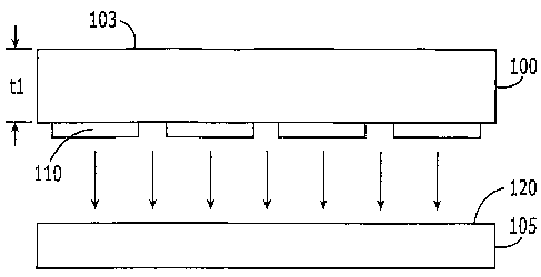
As shown in Figure 1, a wafer (i. e., a substrate) 100 has a thickness (t1) of
about 250 microns to about 400 microns. A plurality of light emitting devices
(LED)
110 are formed on a surface of the wafer 100 that is opposite a backside 103
of the
wafer 100. It will be understood that the plurality of LEDs can be GaN-based
light
emitting diodes that typically comprise an insulating or semiconducting
substrate (or
wafer) such as SiC or sapphire on which a plurality of GaN-based epitaxial
layers are
deposited. The epitaxial layers comprise an active region having a p-n
junction that
emits light when energized. In some embodiments according to the invention,
the
wafer is a SiC wafer of 4H-SiC, 6H-SiC or another type of material known to
those
skilled in the art.
According to Figure 2, in some embodiments according to the invention, a
wafer 100 (including the plurality of LEDs 110) and a wafer carrier 105 are
coupled
together via an adhesive layer 120 in contact with the plurality of LEDs so
that the
entire assembly can be subject to processing by, for example, mounting the
wafer
carrier 105 in a grinder so that the backside 103 of the wafer 100 can be
accessed. It
will be understood that the wafer 100/plurality of LEDs 110 can be coupled to
the
wafer carrier 105 using any technique known to those skilled in the art, such
as a wax,
and may be applied to the plurality of LEDs or to the wafer carrier. It will
be further
understood that the term "contact" includes direct contact as well as indirect
contact
where, for example, one or more intervening elements (such as the adhesive
layer
described above) are present between the plurality of LEDs and the wafer so
that
8
CA 02545628 2006-05-11
WO 2005/048363 PCT/US2004/037934
these two elements can be coupled together and the backside of the wafer can
be
processed while holding the carrier.
According to Figure 3, in some embodiments according to the invention, the
backside 103 of the wafer 100 is processed to reduce the wafer 100 to a
thickness t2,
which is less than t1, to form a thinned wafer 100'. It will be understood
that the
thickness t2 is less than t1 to allow a saw blade having a beveled tip to cut
beneath the
surface of the backside 103 to a depth less than about a length of the bevel
of the tip
of the saw blade. Accordingly, the beveled tip is partially inserted into the
backside
103 so that straight edges of the saw blade can remain exposed above the
backside
103.
In some embodiments according to the invention, the thickness of the wafer
100 is reduced using a grinder, such as an in-feed or creep feed grinder. In
other
embodiments according to the invention, the thickness of the wafer 100 is
reduced
using lapping, chemical or reactive ion etching or combinations of these
approaches
with or without grinding. In still other embodiments according to the
invention,
etching may be used to treat the backside of the thinned wafer (i. e., after
thinning the
wafer) to reduce damage to the wafer so that growth of epi-layers may be
improved.
It will be understood that although the embodiments described above refer to
partial insertion of the beveled tip (so that the straight edges of the saw
blade can
remain exposed), in some embodiments according to the invention, the beveled
tip
may be inserted farther so that a small portion of the straight edges of the
saw blade
are inserted below the surface of the thinned wafer 100'. It will be further
understood
that the LEDs so formed may still provide the substantially the same benefits
as those
embodiments where the beveled tip is partially inserted (such as improved
light
extraction and improved conformal deposition of a phosphor coating thereon).
Accordingly, embodiments where a small portion of the straight edges of the
saw
blade are inserted below the surface of the thinned wafer 100' will be
understood to be
within the scope of the claimed subject matter.
In some embodiments according to the invention, the wafer 100 is thinned to a
thickness of less than about 150 microns. In other embodiments according to
the
invention, the wafer 100 is thinned to a thickness of less than about 120
microns. In
some embodiments according to the invention, the wafer 100 is thinned using an
in-
feed grinder or a creep-feed grinder.
9
CA 02545628 2006-05-11
WO 2005/048363 PCT/US2004/037934
The partial insertion of the beveled tip coupled with the reduced thickness of
the thinned wafer 100' allows the plurality of LEDs to be separated from one
another
by, for example, breaking the thinned wafer 100' rather than cutting through
the entire
wafer. Once the backside 103 has been processed to sufficiently thin the wafer
100',
the wafer carrier 105 can be removed from the assembly by, for example,
heating the
adhesive layer 120 so that the thinned wafer 100' and the plurality of LEDs
thereon
may be removed as shown in Figure 4. In other embodiments according to the '
invention, the wafer carrier 105 can be removed from the assembly using an
appropriate based on the structure used to couple these elements as shown
above in
reference, for example, to Figure 2. For example, the structure may be
dissolved or
melted to separate the wafer carrier 105 from the assembly.
Ohmic contacts 107 can be formed on the backside 103 of the wafer 100'
using, for example, laser annealing as discussed in U.S. Patent Application
SeriaTNo.:
10/916,113, entitled Localized Annealing of Metal-Silicon Carbide Ohmic
Contacts
and Devices So Formed to Slater et al., filed August 11, 2004, which is
commonly
assigned to the present Assignee, the disclosure of which is incorporated
herein by
reference. It will be understood that the ohmic contacts can be formed on the
thinned
wafer 100' while the wafer is coupled to the wafer carrier. In some
embodiments
according to the invention, the ohmic contacts can be formed on the thinned
wafer
100' after the wafer is removed from the wafer carrier, as shown for example,
in
Figure 5. Bonding pads 106 can be formed on the plurality of LEDs 110 opposite
the
ohmic contacts. A saw blade 30 can be used to cut the wafer 100' to separate
the
plurality of LEDs for packaging. It will be understood that the saw blade 30
can cut
through the entire wafer 100' to form straight edges on the thinned wafer 100'
between
the separated plurality of LEDs 110 or substantially through the thinned wafer
100' so
that the LEDs 110 may be separated from one another by applying pressure along
the
score lines formed by the saw blade 30.
In other embodiments according to the invention as illustrated in Figure 6,
the
saw blade 30 is partially inserted into the thinned wafer 100' to a depth that
is less
than the length of the beveled tip 131 to form beveled grooves 17 in the
thinned wafer
100'. The saw 30 is partially inserted into the thinned wafer 100' so that the
straight
edges 31 of the saw 30 remain exposed when the beveled tip 131 is partially
inserted
to avoid the formation of undesirable geometries in the thinned wafer 100'
above the
CA 02545628 2006-05-11
WO 2005/048363 PCT/US2004/037934
beveled grooves 17. Moreover, the thickness of the thinned wafer 100' allows
the
beveled groves 17 to penetrate sufficiently into the thinned wafer 110' so
that the
plurality of LEDs can be separated from one another by breaking the thinned
wafer
100' along grooves (or score lines) as shown in Figure 7. Furthermore, as
discussed
above in reference to Figure 5, bonding pads 106 and ohmic contacts 107 can be
formed on the plurality of LEDs.
In further aspects according to embodiments of the invention, the backside 103
of the wafer 100' can be processed to further improve light extraction from
the LED
including patterning the backside 103 with a laser or by what is commonly
referred to
as "roughing." The laser patterning may be provided in a single or step-wise
fashion.
By patterning the backside 103, light extraction may be improved, for example,
by
providing a randomization pattern thereon. Embodiments of the invention may be
particularly well suited to larger area devices where the effectiveness of
angled
sidewalls of the wafer 100' may be reduced because of the surface area of the
device.
Furthermore, one or both of the opposing faces of the wafer 100' (i. e., a
front side and
the backside 103) may be patterned. The wafer 100' may be patterned using a
laser
patterning system such as that described in U.S. Patent Application Serial No.
101815,293, entitled Laser Patterning of Light Emitting Devices and Patterned
Light
Emitting Devices to Donofrio, filed April 1, 2004, the entire disclosure of
which is
incorporated herein by reference.
In some embodiments of the invention, the laser used to pattern the wafer 100'
is an excimer pulsed laser, however any laser system suitable for removing
material
from the substrate may be used. For example, the laser system could be a
frequency
tripled andlor quadrupled YAG laser. In certain embodiments of the invention,
the
25~ laser has a wavelength of 308 nm, however, other wavelengths, such as 248
nm, 193
nm, 157 nm, 355 nm or 266 nm could also be used. Additionally, assist
processes
known to those of skill in the art could also be employed to mitigate surface
damage
and/or enhance laser absorption, such as water mist and/or assist gases.
Multiple
pulses of the laser may be used to remove material from the substrate. Any
energy
suitable for controllably removing material from the substrate may be used.
For
example, a pulsed 308 nm laser of about 4.2 J/pulse may be used in certain
embodiments of the present invention.
11
CA 02545628 2006-05-11
WO 2005/048363 PCT/US2004/037934
Figure 8 is a cross-sectional view of an LED on the wafer 100' having the
backside 103 laser patterned according to some embodiments of the invention.
Figure
9 is an isometric pictorial view of the light-emitting device of Figure 8.
Three-
dimensional patterns 120 are formed in the backside 103 using a laser as
described
above. In the embodiments illustrated in Figures 8 and 9, the LED 110 is
formed on
an opposite side 104 (i. e., front side) of the wafer 100'. As is seen in
Figures 8 and 9,
the patterns 120 are surrounded by an uninterrupted perimeter 130 on the
backside
103 of the wafer 100.
Figures 10 and 11 are cross-sectional views of wafers 100' according to
further
embodiments of the present invention. As seen in Figures 10 and 1 l, in cross-
section,
curved surfaces extending into 200 or protruding 210 from the wafer 100' may
be
provided by laser patterning. The curved surfaces 200, 210 may include a
parabolic
curve. Such a curve may be provided, for example, by controlling the laser
light
using a series of masks that provided the selective removal of substrate
material to
provide the parabolic structures. In certain embodiments of the present
invention, the
curved surfaces may provide lenses in the substrate. In other embodiments of
the
present invention, the curved surfaces may provide a sinusoidal pattern of
grooves.
While multiple curved structures are illustrated in Figures 10 and 1 l, the
wafer
100' could be shaped to a single curve so as to provide a curved wafer 100'.
The
. curved wafer 100' may be curved on both faces. Also, the light emitting
device could
be provided on the curved surface of the wafer 100'.
Figures 12 and 13 are cross-sectional views of wafers 100' according to
fiuther
embodiments of the invention. As seen in Figures 12 and 13, combinations of
curved
220 and non-curved features 230, 240 may be provided in a single wafer 100'.
Thus,
embodiments of the invention may include multiple different three-dimensional
geometric patterns in a single wafer 100'.
Figures 14 through 16 illustrate alternative embodiments for laser patterning
according to some embodiments of the invention. As seen in Figure 14, a
polymer
mask layer 300 may be provided on the wafer 100'. In Figure 15, the polymer
mask
layer 300 is laser patterned to provide a polymer mask 310 having three-
dimensional
features 320 corresponding to features to be provided in the wafer 100'. In
Figure 16,
the mask 310 is used as an etch mask and the wafer 100' is etched to provide
the
three-dimensional features 330. The etch may, for example, be a dry etch.
12
CA 02545628 2006-05-11
WO 2005/048363 PCT/US2004/037934
Conventional polymer masks and techniques for etching using polymer masks may
be
used. Additionally, other mask materials that may be laser patterned could
also be
used.
Techniques for laser patterning a polymer layer are known to those of skill in
the art. For example, such techniques are described in "Laser micro-machining
of
high density optical structures on large substrates" by Boehlen et al. of
Exitech Ltd.
In particular embodiments of the invention, where the etching mask is a
polymer
etching mask, the polymer may be patterned with a 248 nm laser.
Characteristics of the etching process may be taken into account in designing
the
characteristics of the mask 310 to provide a desired three-dimensional
geometric
pattern in the wafer 100'. For example, the differences in etch rate between
the mask
material and the silicon carbide wafer may be taken into account when the mask
is
patterned.
Because the patterning of the etching mask is provided for by laser
patterning,
the shape of the etching mask may be readily adjusted through control of the
laser
mask. Thus, for example, the shape of the etching mask may take into account
the 6
to 1 etching rate of the etching mask to the silicon carbide and the features
adjusted
accordingly. Such an adjustment of mask characteristics may be difficult to
provide
without the use of laser patterning of the etching mask. Furthermore, through
utilization of laser patterning, multiple geometries, e.g., pyramids and
lenses can be
formed in a single step with scanning image technique by designing them into
the
laser mask.
Additionally, the surface of the wafer after the etch may be rough or smooth.
A roughened surface may be provided, for example, by placing a thin layer of
material, such as aluminum, between the etch mask and the substrate to create
a
micro-mask. When etched, the micro-mask may act to roughen a surface of the
wafer
100'.
Many alterations and modifications may be made by those having ordinary
skill in the art, given the benefit of the present disclosure, without
departing from the
spirit and scope of the invention. Therefore, it must be understood that the
illustrated
embodiments have been set forth only for the purposes of example, and that it
should
not be taken as limiting the invention as defined by the following claims. The
following claims are, therefore, to be read to include not only the
combination of
13
CA 02545628 2006-05-11
WO 2005/048363 PCT/US2004/037934
elements which are literally set forth but all equivalent elements for
performing
substantially the same function in substantially the same way to obtain
substantially
the same result. The claims are thus to be understood to include what is
specifically
illustrated and described above, what is conceptually equivalent, and also
what
incorporates the essential idea of the invention.
14