Note : Les descriptions sont présentées dans la langue officielle dans laquelle elles ont été soumises.
CA 02550776 2006-06-21
WO 2005/064737 PCT/SE2003/002091
1
Title:
TUNABLE MICROWAVE ARRANGEMENTS
FIELD OF THE INVENTION
The present invention relates to a tunable microwave arrangement
comprising a microwave/integrated circuit device and a substrate.
The invention also relates to a method for tuning such a microwave
arrangement.
STATE OF THE ART
In advanced microwave communications systems the requirements on
components are getting higher and higher e.g. as far as
performance and functionality are concerned. For the functionality
reconfigurability, flexibility and adaptability are important
issues. Fabrication costs are also critical issues. Another
important factor is the need to be able to make various microwave
components as small as possible.
Therefore a large effort is put on finding new and better
materials for the making of the components. Another critical issue
concerns design methods and much investigation is done to refine
existing methods and to establish new, improved design methods.
Recently Electromagnetic BandGap (EBG) crystals, also denoted
photonic bandgap crystals, have been proposed for the design of
microwave devices and microwave systems, particularly for the
purposes of providing improved performance. This is e.g. discussed
in "PBG Evaluation for Base Station Antennas", in 24th ESTEC
Antenna Workshop on Innovative Periodic Antennas. Photonic
CA 02550776 2006-06-21
WO 2005/064737 PCT/SE2003/002091
2
Bandgap, Fractal and Frequency Selective structures (WPP-185),
pages 5-10, 2001.
It has also e.g. in "Beam steering microwave refector based on
elecrically tunable impedance surfaces", by D.Sievenpiper,
I.Schaffner, Electronics Letters, Vol. 38, no. 21, pages 1237
1238, 2002 been demonstrated that microstrip devices with EBG
frequency sectiv-e surfacer offer improved performances as far as
the suppression of surface waves is concerned. In this same
document it is pointed at the possibility of tuning EBG crystals
using semiconductor varactoxs. However, it is actually not
possible to use such types of tunable EBG crystals as ground
planes for several reasons. One reason is that the use of
semiconductor diodes makes the design expensive.
Another reason is that the sizes of the EBG crystals are
comparable to the wavelenght of the microwaves, which makes it
impossible to use them as groundplanes in some microwave devices
(e.g. microstrip filters). Still further the tuning DC voltage is
applied to the top microstrip circuit.
The supply of the tuning DC-voltage however requires decoupling
circuits to prevent the microwaves from going into the DC supply.
It must be possible to permit the DC supply to be delivered to the
microwave component (e. g. microstrip). Such decoupling circuits
however make the entire microwave device/circuit complicated.
Moreover, sometimes they require high voltages which may make the
device dangerous, and other components may be vulnerable to such
high voltages.
One way to overcome the problems associated with decoupling
circuits might be to move controlled components from the top
surface to the bottom surface of the device. This may however be
complicated and inconvenient for several applications.
CA 02550776 2006-06-21
WO 2005/064737 PCT/SE2003/002091
3
SUMMARY OF THE INVENTION
What is needed is therefore a microwave arrangement as initially
refered to which has a high performance and which is flexible.
Still further a microwave arrangement is needed which is cheap and
easy to design and fabricate. Further yet a microwave arrangement
is needed which is adaptable and reconfigurable. Particularly an
arrangement is needed which is tunable without requiring much, or
any at all, complicated and risky decoupling circuits requiring
high voltages. Even more particularly a microwave arrangement is
needed through which advantage can be taken of e.g.
Electromagnetic Bandgap crystals as ground planes without
requiring high voltage decoupling circuits. Microwave arrangements
are also needed which are small sized, easy to tune and which can
be used for high frequency (GHz and above that) applications, e.g.
within modern microwave communication systems and radar systems,
among others. A method for tuning such an arrangement is also
needed.
Therefore a microwave arrangement as initially referred to is
provided which comprises a layered structure disposed between said
microwave/integrated circuit device and said substrate, which
layered structure acts as a ground plane. It comprises at least
one regularly or irregularly patterned first metal layer, at least
one second metal layer and at least one tunable ferroelectric film
layer. The layers are so arranged that the/a ferroelectric film
layer is/are provided between the/a first metal layer and the/a
second metal layer.
Preferably the patterned first metal layers) comprises) (a)
patterned Elecromagnetic Bandgap crystal structure. The
ferroelctric film layers) may be patterned in some
CA 02550776 2006-06-21
WO 2005/064737 PCT/SE2003/002091
4
implementations. However, in other implementations the
ferroelectric film layers) is/are homogeneous, i.e not patterned.
The second metal layers) may be homogeneous, i.e not patterned,
but it may also be patterned. It may then be differently patterned
than the ferroelectric layer (if patterned) or in the same manner.
It may also be differently or similarly patterned as compared to
the first metal layer. By patterned is in this application meant
any regular or irregular patterning. It may comprise stripes,
squares (one or more), rectangles, ovals, circular patterns or
anything.
The second metal layers) particularly comprises) Pt, Cu, Ag, Au
or any other appropriate metal.
The ferroelectric film layer may comprise SrTi03, BaX Srl_X Ti03 or
a material with similar properties.
The ground plane structure is tunable, and for tuning a DC voltage
is applied between the/a first metal layer and the/a second metal
layer. If there are more first and second layers, i.e. a
multilayer structure, any appropriate first and second layers may
be selected for tuning purposes.
Tuning of the microwave/integrated circuit device is achieved
through the tuning of the ground plane, particularly without
requiring any decoupling circuits on the device at all.
Through the application of the DC biasing (tuning) voltage, the
dielectric constant of the ferroelectric film is affected,
changing the impedance of the ground plane surface adjacent the
microwave/integrated circuit device, thus tuning the device or
component arranged on the ground plane, preferably with a
dielectricum (e.g of BCB) disposed therebetween.
The microwave circuit may comprise a microstrip line or coupled
microstrip lines. It may also comprise a patch resonator (of any
appropriate shape, square, circular, rectangular etc.). In another
embodiment the microwave circuit comprises an inductor coil. It
CA 02550776 2006-06-21
WO 2005/064737 PCT/SE2003/002091
may also generally comprise a microwave transmission line, or e.g.
a coplanar strip line device.
As can be seen, the microwave/integrated circuit device may in
principle comprise any component, e.g. a semiconductor IC, parts
5 of filters, e.g. bandpass or bandreject filters etc.
The substrate may comprise a semiconductor, e.g. Si, a
dielectricum, a metal or any material with similar properties.
As referred to above, between the microwave device and the (top)
patterned first metal layer a low permittivity, low loss
dielectricum is preferably provided, which comprises a BCB or any
other polymer. Preferably the applied tuning voltage is lower than
100 V, even more particularly lower than about 10 V, e.g. 5 V.
The ferroelectric layer may have a thickness of about 0.1-2 f.~m.
Particularly the ground plane structure comprises a multilayer
structure with more than one ferroelectric layer, each
ferroelectric layer being disposed between a first and a second/a
first metal layer.
The invention also proposes a method for tuning a microwave
arrangement comprising a microwave/integrated circuit device and a
substrate. The microwave arrangement further comprises a layered
structure acting as a ground plane for the arrangement and being
disposed between the microwave/integrated circuit device and the
substrate, the method comprising the step of; applying a DC tuning
voltage between a first patterned metal layer and a second metal
layer disposed on opposite sides of a ferroelectric layer, which
layers constitute the ground plane of the arrangement.
Preferably the patterned first metal layers) comprises) a
patterned Electromagnetic Bandgap crystal structure.
For tuning the microwave/integrated circuit device, the step of
applying a DC voltage influences the impedance on top of the
ground plane, thus changing the resonant frequency of the
microwave/integrated circuit device.
CA 02550776 2006-06-21
WO 2005/064737 PCT/SE2003/002091
6
The method particularly further comprises the step of, in a
multilayered ground plane structure comprising more than two
ferroelectric film layers; selecting any of the first and second
metal layers surrounding any of the ferroelectric films for tuning
the microwave/integrated circuit device.
BRIEF DESCRIPTION OF THE DRAV~IINGS
The invention will in the following be further described, in a
non-limiting
manner, and
with reference
to the accompanying
drawings, in which:
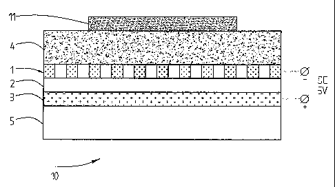
Fig. 1 is a cross-sectional view of a microwave arrangement
with a tunable EBG ground plane,
Fig. 2 is a plan view of another embodiment according to the
invention in which the microwave device comprises a
circular patch reonator,
Fig. 3 is a plan view of still another embodiment wherein the
microwave device comprises coupled microstrip lines,
Fig. 4 is a plan view of still another embodiment wherein the
microwave device comprises a tunable inductor coil,
Fig. 5 is a cross-sectional view of an arrangement according
to the invention according to still another embodiment,
and
Fig. 6 shows an arrangement according to the invention wherein
the ground plane comprises a multilayer structure
wherein first and second layers are selected for tuning
purposes.
DETAILED DESCRIPTION OF THE INVENTION
Fig. 1 shows a microwave arrangement 10 accordning to one
embodiment of the invention. The microwave arrangement 10
comprises a microwave device 11 here comprising e.g. a patch
CA 02550776 2006-06-21
WO 2005/064737 PCT/SE2003/002091
7
resonator and a substrate 5 e.g. of Si. A layered structure
forming a ground plane is disposed on the substrate 5 and it
comprises a first metal layer 1, here comprising an EBG patterned
on top of a ferroelectric film layer 2 which is tunable.
Ferroelectric films have been proposed for microwave applications
in US-A-6 187 717. In this document. it is established that
ferroelectrics having a large dielectric constant enable a
substantial reduction in size and the DC voltage dependence of
the permittivity. This makes ferroelectric materials extremely
advantageous for applications where it is desirable to have small
sized tunable microwave devices. This document is herewith
incorporated herein by reference.
The ferroelectric film layer 2 may e. g. comprise SrT~i03, Bax Srl-x
Ti03 or any other material with similar properties. The
ferroelectric film is disposed on a second metal layer 3, here
e.g. comprising Pt (or Cu, Au, Ag etc). The first metal layer 1
is patterned. It may be regularly patterned or irregularly
patterned. In this implementation it is regularly patterned to
form stripes with a pitch of e.g. ~,g/2 (the wavelength in the
medium) or smaller than that. Preferably it comprises 2D EBG
material.
The ferroelectric film layer 2 shown in this embodiment is not
patterned. It may however also be patterned, in the same manner
as the first metal layer 1, or in any other manner. The patch
resonator 11 (or any other passive microwave component) is
separated from the EBG surface (i.e. the top surface of the
first, patterned metal layer 1) through a low permittivity, low
loss dielectricum 4, e.g. of BCB or any other polymer (or any
other material with similar properties).
For tuning of the microwave component (here patch resonator 11) a
tuning voltage (of less than 100 V, preferably less than 10, e.g.
5 V) is applied between the first metal layer 1 and the second
metal layer 3 (the ground plane). Tuning the impedance of the EBG
CA 02550776 2006-06-21
WO 2005/064737 PCT/SE2003/002091
8
ground plane will change the resonant frequency of the patch
resonator 11.
The design may e.g. be integral with a Si IC circuit, and it is
useful among others for high frequencies, e.g. up to and above
about 20 GHz.
It should be noted that the microwave device (here patch resonator
11) is not DC biased, but instead the first and second metal
layers where the tuning of the surface of the ground plane is
achieved, and hence of the resonant frequency.
Fig. 2 shows an arrangement 20, quite similar to that of Fig. 1 in
a plan view, from above. It discloses a microwave device 12
comprising a circular patch resonator on top of a dielectric
layer e.g. of BCB (not shown in the Figure). The dielectric layer
is disposed on a first metal layer 1' comprising a 2D EBG
patterned crystal layer and it here comprises orthogonal strips.
The ferroelectric film layer on which the first metal layer is
disposed is not visible in the Figure, neither is the second
metal layer. However, the structure substantially corresponds to
that of Fig. 1. The ground plane is disposed on substrate layer
5', e.g. of Si. It should be clear that the patch resonator does
not have to be circular, on the contrary it might have any
appropriate shape, there might be more than one patch etc.
Fig. 3 shows a plan of view of a microwave arrangement 30
comprising a microwave device in the form of coupled microstrip
lines 13, 13 provided on a dielectricum (not shown) which is
disposed on a tunable ground plane as in Fig. 1, of which only
the patterned first metal layer 1" is shown. The ground plane is
disposed on a Si (here) substrate layer 5" . The arrangement 30
may e.g. form part of tunable bandpass filter. Tuning is achieved
in accordance with Fig. 1.
CA 02550776 2006-06-21
WO 2005/064737 PCT/SE2003/002091
9
Fig. 4 is a plan view of an alternate microwave arrangement 40
comprising a microwave/integrated circuit device in the form of a
lumped inductor coil 14 disposed on a dielectricum (not shown)
disposed between the inductor coil 14 and a tunable ground plane
according to the invention~(cf. Fig. 1) of which only the first,
patterned (2D EBG) metal layer 1" ' is shown. The ground plane is
provided on a substrate 5"' . The functioning is similar to that
described with reference to Fig. 1 and through applying of a DC
voltage to the first and second metal layers, the surface of the
ground plane will be tuned and thus the inductance of the
inductor coil 14 will be tuned.
Fig. 5 is a view in cross-section of a microwave arrangement 50.
The microwave device comprises coupled microstrips 15, 15, 15
disposed on a dielectricum 44. The dielectricum 44 is arranged on
a ground plane which here comprises, on top, a patterned first
metal layer 14 , a ferroelectric film layer 24, which in this
embodiment also is patterned, and which in turn is arranged on a
second metal layer 34, which in this particular embodiment also is
patterned. The ground plane is provided on a substrate 54. Tuning
is achieved through application of a tuning voltage V to the
first and second metal layers.
Finally Fig. 6 is a cross-sectional view of still another
inventive arrangement 60. It comprises here a patch resonator 16
provided on a dielectricum 45. However, the ground plane here
comprises, in turn from the top, a patterned first metal layer 15,
a ferroelectric layer 25, another patterned first metal layer 16,
a further ferroelectric layer 26 and a second metal layer 35. The
layered structure is disposed on a substrate 55. In the shown
embodiment the tuning voltage is applied to the top first metal
layer 15 and the the second metal layer 35. It could however also
have been applied to the first metal layer 16 and the second
CA 02550776 2006-06-21
WO 2005/064737 PCT/SE2003/002091
metal layer 35, or to the first metal layer 15 and the other first
metal layer 16. Any variation is in principle possible. There
might also be still more first and second metal layers, and
ferroelectric layers.
5
It should be clear that the invention of course not is limited to
the specifically illustrated embodiments, but that it can be
varied in a number of ways within the scope of the appended
claims.
15
25