Note : Les descriptions sont présentées dans la langue officielle dans laquelle elles ont été soumises.
", ,..."y, ,..,.~.,",.,,".a,",.,».1.~.".....4,,.
CA 02552086 2006-07-14
MICROENGINEERED NANOSPRAY ELECTRODE SYSTEM
Field of the Invention
This invention relates to mass spectrometry, and in particular to the use of
mass spectrometry
in conjunction with liquid chromatography or capillary electrophoresis. The
invention
particularly relates to a system and method that is implemented in a
microengineered
configuration.
Background
Electrospray is a common method of soft ionisation in biochemical mass
spectrometry (MS),
since it allows the analysis of fluid samples pre-separated by liquid
chromatography (LC), the
ionization of complex molecules without fragmentation, and a reduction in the
mass-to-
charge ratio of heavy molecules by multiple charging [Gaskell 1997; Abian
1999]. It may be
used in a similar way with fluid samples pre-separated by other methods such
as capillary
electrophoresis (CE).
The principle is simple. A voltage is applied between an electrode typically
consisting of a
diaphram containing an orifice and a capillary needle containing the analyte.
Liquid is
extracted from the tip and drawn into a Taylor cone, from which large charged
droplets are
emitted. The droplets are accelerated to supersonic speed, evaporating as they
travel.
Coulomb repulsion of the charges in the shrinking droplet results in
fragmentation to ions
when the Rayleigh stability limit is reached. The resulting ions can be
multiply charged.
An electrospray mass spectrometer system contains a number of key elements:
~ An electrospray ionisation source capable of interfacing to an LC or CE
system
~ An interface to couple ions (in preference to molecules) into a vacuum
chamber
~ An alignment and/or observation system capable of maximising the coupling
~ A mass filter and detector
Conventionally, the spray is passed from atmospheric pressure via a chamber
held at an
intermediate pressure. Several vacuum interfaces that use differential pumping
to match flow
rates to achievable pressures have been developed [Duffin 1992]. The ion
optics normally
1
~.. ,.,,.,.*"ni,m, i...~...n.e...d...m....4..
CA 02552086 2006-07-14
consist of input and output orifices such as capillaries, capillary arrays and
skimmer
electrodes, and occasionally also a quadrupole lens operating as an ion guide
in all-pass
mode. These components are used to maximise the ratio of coupled ions to
neutrals, which
would otherwise swamp the chamber.
Various methods are used to promote a well-dispersed spray of small droplets
and hence a
concentrated flow of analyte ions. Solvent can be preferentially driven off,
by direct heating
[Lee 1992]. Advantages may be obtained by the use of a sheath gas flow
[Huggins 1993], and
nebulisation may be enhanced by ultrasound [Hirabayashi 1998].
Alignment in electrospray is not critical, and the spray may simply be
directed towards the
MS input. Alternatively, an off-axis spray direction may be used to promote
the separation of
neutrals. Co-axial lenses mounted directly on the capillary have been
developed to focus the
spray [US6462337]; however, there are limits to the electrode complexity that
can be
achieved using such simple mechanical systems.
In a conventional electrospray system, with capillaries of 100 pm internal
diameter, flow
rates are of the order of 1 ~1 miri 1, and extraction voltages lie in the
range 2.5 kV - 4 kV.
Flow rates and voltages are considerably reduced in so-called "nanospray
systems", based on
capillaries having internal diameters ranging down to ~10 pm [Wilm 1996]. Such
capillaries
are relatively easy to fabricate, and are available with a range of diameters
and frits.
Decreasing the capillary diameter and lowering the flow rate also tends to
create ions with
higher mass-to-charge ratio, extending the applicability further towards
biomolecules.
Because of the reduced size of the spray cone, alignment of a nanospray source
is more
critical. Operation typically involves mounting the source on a
micropositioner and using a
video camera to observe the spray entering the vacuum inlet of an atmospheric
pressure
ionisation (API) mass spectrometer. Sources are sold customised for most
popular brands of
mass spectrometer. However, such systems are large, complex and costly.
To reduce costs, a variety of attempts have been made to integrate some of the
components of
nanospray ionisation sources. Ramsey and Ramsey [ 1997] showed that a spray
could be
2
" , a ,*,...,*~rv ~",i"~,..,a."»,.~ .n "
CA 02552086 2006-07-14
drawn from the edge of a glass chip containing an etched capillary. Since
then, integrated
capillaries with in-plane flow have been demonstrated in many materials,
especially plastics
[Licklider 2000; Svedberg 2003]. In some cases, the fluid has been extracted
from a slot
rather than a channel [Le Gac 2003]; in others, from a shaped surface [Kameoka
2002].
Devices have also been formed in one-dimensional arrays. Geometries in which
the flow is
passed perpendicular to the surface of the chip have also been demonstrated,
often by deep
reactive ion etching of silicon [Schultz 2000; Griss 2002]. Such devices may
be formed into
two-dimensional arrays.
Almost exclusively, the advances above consist of attempts to integrate system
sub-
components leading up to the ion emitter. They concentrate on the fluidic part
of the system,
ignoring the problems of separating ions from neutrals, and of aligning the
ion spray to the
inlet to the vacuum system. As a result, they are not suitable for a low cost
nanospray system,
because accurate alignment still requires expensive positioning devices.
There is therefore a need to provide a low cost nanospray system.
summary
Illustrative embodiments of the invention address these and other problems by
providing a
solution to the problems of alignment and electrode mounting in a low-cost
nanospray source
by using microelectromechanical systems technology to form appropriate
mechanical
alignment and conducting electrode features on insulating plastic substrates
in an integrated
manner. The approach also allows integration of features for fluid drainage,
spray heating and
sheath gas flow.
Illustrative embodiments of this invention provide a method of aligning a
nanospray capillary
needle, a set of electrodes, and the capillary input to an API mass
spectrometer. The electrode
system is formed using microelectromechanical systems technology, as an
assembly of two
separate chips. Each chip is formed on an insulating plastic substrate. The
first chip carries
mechanical alignment features for the capillary electrospray needle and the
API mass
spectrometer input, together with a set of partial electrodes. The second chip
carries a set of
partial electrodes. The complete electrode system is formed when the chips are
assembled in a
3
,, e...,A~ .,.~.,."~,, i,..,y.,»u..,A.ru...,...H,.,.
CA 02552086 2006-07-14
stacked configuration, and consists of an einzel lens capable of initiating a
Taylor cone and
separating ions from neutrals by focusing.
Accordingly, an illustrative embodiment of the invention provides a system
according to
claim 1 with advantageous embodiments provided in the dependent claims
thereto. An
illustrative embodiment of the invention also provides a method of fabricating
such a system
as detailed in the main independent method claim.
1n accordance with one such illustrative embodiment of the invention, there is
provided a
microengineered nanospray ionisation device provided on a single chip for
coupling between
a nanospray source and a mass spectrometer. The device includes a first
alignment feature for
cooperating with a capillary input, a second alignment feature for cooperating
with a capillary
output and an orifice defining an ion path between the capillary input and
capillary output.
The device fiu-ther includes at least one conducting electrode provided in an
orientation
substantially perpendicular to the ion path. Each of the first alignment
feature, the second
alignment feature, the orifice and the at least one electrode are integrally
formed in the chip.
In accordance with another illustrative embodiment of the invention, there is
provided an
integrated package including a nanospray source having a capillary needle at
an output
thereof, a mass spectrometer having a capillary needle at an input thereof and
a nanospray
ionisation device as described herein provided between the source and the mass
spectrometer.
The alignment features of the device provide connection ports for the
capillary needles so as
to enable a fluid originating from the source to be ionised and passed to the
mass
spectrometer.
These and other features will be better understood with reference to the
following drawings.
Brief Description of the Drawings
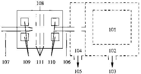
Figure 1 shows in schematic form a microengineered nanospray system aligning a
nanospray
needle with the capillary input to an atmospheric pressure ionisation mass
spectrometer
according to an embodiment of the present invention.
4
". ,. . a ". """.,. . , M ~.,~.,,"~,~,.,.,.."~.."..
CA 02552086 2006-07-14
Figure 2 shows construction of a microengineered nanospray system as a stacked
assembly of
two chips according to an embodiment of the present invention.
Figure 3 is a process flow for construction of a microengineered nanospray
chip according to
an embodiment of the present invention.
Figure 4a shows the layout of a lower and Figure 4b the layout of an upper
substrate of a
microenginered nanospray chip according to an embodiment of the present
invention.
Figure 5 shows an assembly of a microengineered nanospray chip according to an
embodiment of the present invention.
Figure 6 shows electrostatic operation of a microengineered nanospray chip
according to an
embodiment of the present invention.
Figure 7 shows operation of the sheath gas inlet of a microenginered
electrospray chip
according to an embodiment of the present invention.
Figure 8 shows thermal operation of a microengineered electrospray chip
according to an
embodiment of the present invention.
Figure 9 shows electrode configurations realisable using a stacked electrode
assembly with
Figure 9a) being a closed pupil arrangement, Figure 9b) a horizontally split
pupil, Figure 9c) a
vertically split pupil and Figure 9d) a quadrant pupil arrangement.
Detailed Description of the Drawings
The invention will now be described with reference to exemplary embodiments as
provided in
Figures 1 to 9.
The present inventor has realised that the benefit of MEMS structures can be
extended to
nanospray applications. In MEMS, widely used methods of lithographic
patterning, oxidation
and metallisation are combined with specialised techniques such as anisotropic
wet chemical
etching [Bean 1978] and deep reactive ion etching [Hynes 1999] to form three-
dimensional
features in crystalline semiconductors such as silicon. UV exposure of
specialised
photosensitive polymers such as SU-8 may be used to form three-dimensional
features in
plastics [Lorenz 1997]. These methods may be used to combine insulating
substrates,
alignment features and conducting electrodes. The present inventor has
realised that at least
potentially, they may therefore form an integrated nanospray ionisation source
at low cost.
5
_. ,..."_. ~1, ,.".,»~,. , ", d ,u....d....,.,.. , d ...
CA 02552086 2006-07-14
However, further difficulties remain with the realisation that MEMS technology
could be
used to provide nanospray devices. The device must typically operate with high
voltages, in a
wet environment, so that electrical isolation and drainage are both required.
The substrate
material most commonly used in MEMS, silicon, is therefore not appropriate;
however, other
insulating materials such as glasses are difficult to micromachine. To obtain
a stable spray, an
electrode containing an axially aligned orifice is typically required. To
obtain efficient ion
separation from neutrals, electrostatic deflection or focusing is required.
For focusing, further
electrodes containing aligned orifices are needed. If the ion path is itself
in the plane of a
substrate, such orifices are extremely difficult to form by in plane
patterning alone. Finally, it
is desirable to integrate features capable of providing a sheath gas around
the spray, of
promoting nebulisation, and of preferentially evaporating solvent. For these
and other reasons
there has heretofore not been possible an integrated MEMS nanospray system.
However, as
will be understood from a review of Figures 1 to 9, the present inventor has
addressed these
and other issues.
Figure 1 illustrates the concept of a microengineered nanospray electrode
system. A mass
spectrometer 101 is provided in a high-vacuum enclosure 102 pumped (for
example) by a
turbomolecular pump 103. Ions are channelled into this chamber via a further
chamber 104
held at an intermediate pressure and pumped (again, for example) by a rotary
pump 105. The
inlet to the vacuum system is assumed to be a capillary 106. The exact
configuration of these
components is not, it will be appreciated, important, apart from the input
capillary. For
example, the filter element of the mass spectrometer could be an ion trap, a
quadrupole, a
magnetic sector, a crossed-field or a time of flight device. Equally, the
intermediate vacuum
chamber could contain a range of components including further capillaries and
skimmer
electrodes.
The overall input to the system is provided by a nanospray capillary 107.
Alignment between
the nanospray capillary 107 and the capillary input to the mass spectrometer
106 is provided
by a rnicroengineered chip 108. The chip contains a first set of mechanical
alignment features
109 for the nanospray capillary and a second set of alignment features 110 for
the capillary
input to the mass spectrometer. The chip also contains a set of electrodes 111
set up
6
.. ..,..L..,...w... ~,..~-M.Ma.......,.1".
CA 02552086 2006-07-14
perpendicular to the ion path, which may (for example, but not exclusively)
consist of
diaphragm electrodes. Other features may be integrated on the chip, including
holes for
drainage and gas inlet.
Figure 2 illustrates the main features of the chip 108. The chip is
constructed from two
separate substrates, each carrying microengineered features, which are
arranged in a stacked
assembly. The first substrate consists of a base 201 formed in insulating
material and carrying
a mechanical alignment feature for the nanospray capillary corresponding to
the feature 109
in Figure 1, which may (for example, but not exclusively) consist of a groove
202 etched into
a conducting or semiconducting block 203. This substrate also carries an
alignment feature
for the capillary input to the mass spectrometer corresponding to the feature
110 in Figure 1,
which may again for example consist of a further groove 204 etched into a
block of similar
material 205. This substrate also carries a set of electrodes corresponding to
part of the
features 111 in Figure 1 and consisting of grooves 206 etched into upright
plates of similar
materia1207.
The second substrate again consists of a base 208 formed in insulating
material, and carrying
a further set of electrodes corresponding to a further part of the features
111 in Figure 1 and
consisting of grooves 209 etched into upright plates of conducting or
semiconducting material
210. When the two substrates are stacked together, the partial electrode sets
combine to form
complete diaphragm electrodes with closed pupils 211.
Using three such electrodes, a so-called 'einzel' or unipotential
electrostatic lens is formed.
This type of lens allows focusing of ions passing axially through the stack of
electrodes in a
simple and controlled manner, and hence allows the ion spray to be focused
onto the capillary
input to the mass spectrometer to present a concentrated stream of analyte
ions.
It will be appreciated that the alignment grooves 202 and 204, and the
electrode grooves 206
and 209, may all be defined by similar photolithographic processes, and may
therefore be
registered together. This aspect provides a solution to the first problem
identified above in the
Background to the Invention section, of constructing an accurately aligned set
of mechanical
features and electrodes. It will also be appreciated that the use of an
insulating substrate that
7
.... ". ,....."1....".~,~.,"."~.... "-,~........."lw.~,".~....~...,.,.
CA 02552086 2006-07-14
may be patterned with drain holes provides a solution to the problem of
maintaining high
voltages in a wet environment. Finally it will be appreciated that a stacked
combination of
partial electrodes provides a solution to the problem of forming diaphragm
electrodes
arranged normal to a substrate.
It will be appreciated by those skilled in the art that a variety of materials
and processes and
may be used to realise structures similar to Figure 2. Figure 3 shows a
process, which is
intended to be exemplary rather than exclusive. The materials used are low
cost, and only
three lithographic steps are required. The process is based on crystalline
silicon substrates on
which plastic virtual substrates are subsequently formed. The individual
process steps are
indicated by a set of evolving wafer cross-sections containing typical
features.
In step 1, a (100)-oriented silicon substrate 301 is first oxidised to form a
Si02 layer 302 on
both sides. The Si02 is patterned and etched to form a channel-shaped opening
303, by (for
example) photolithography and reactive ion etching. In step 2, the underlying
silicon substrate
is anisotropically etched down (111) crystal planes to form a V-shaped groove
304.
Commonly an etchant consisting of potassium hydroxide (KOH), water and
isopropanol
(IPA) may be used for this purpose. This step defines all capillary-mounting
grooves and
electrode pupils. The front side oxide is removed, and the wafer is turned
over.
In step 3, the wafer is spin coated with a thick layer of the epoxy-based
photoresist SU-8 305.
This resist may be coated and exposed in layers of at least 0.5 mm thickness,
has excellent
adhesion, and is extremely rugged after curing, allowing it to be used as a
virtual substrate
material after processing. The resist is lithographically patterned to form a
dicing groove 306
around each die, together with any drain holes 307 and gas inlets.
In step 4, the front side of the wafer is metallised to increase conductivity,
typically with an
adhesion layer of Cr metal and a further thicker layer of Au 308. In step 5,
the front side of
the wafer is coated in a photoresist 309. Since the wafer is non-planar, an
electrodeposited
resist is used in preference to spin-coated resist for this step. The resist
is patterned to define
the outlines of all electrode and alignment blocks 310, and the pattern is
transferred through
the metal. In step 6, the pattern is transferred through the silicon wafer by
deep reactive ion
8
. , ..-.. .~.~., _,.""..,.. ".,"~*,..,,~."..,.,~.,..
CA 02552086 2006-07-14
etching, to form deep separation features 311 between elements. The
photoresist is then
removed, and individual dies are separated in step 7.
In step 8, two dies are stacked together to form a complete nanospray chip, by
soldering or
bonding the metal layers 312 together. Alternatively, a conducting epoxy may
be used for this
step. The chip is mounted on a carrier circuit board, and wirebond connections
313 are made
to appropriate features on the lower substxate.
It will be appreciated by those skilled in the art that a first alternative
process is offered by
forming the conducting alignment and electrode elements by electroplating a
metal inside a
mould, which may itself be formed by a sequence of patterning and etching
steps. However,
this alternative requires the separate formation of a mould, which is a
laborious process.
It will also be appreciated by those skilled in the art that a second
alternative process is
offered by forming the alignment and electrode elements by sawing or otherwise
eroding a
conducting layer attached to an insulating substrate. The substrate bases may
be also defined
by sawing or by erosion, and the grooves may be formed, by partial sawing.
However, this
alternative offers less flexibility in the range of structures that may be
created.
It will also be appreciated by those skilled in the art that a third
alternative process is offered
by forming the substrate bases from glass, which may be patterned by sawing or
(in the case
of a photosensitive glass) by photopatterning. However, these alternatives
again offer less
flexibility in the range of structure that may be created. It will be
appreciated that regardless
of their shortcomings that each of the mentioned alternatives may be
considered useful in the
context of the present invention for specific applications.
Figure 4 shows the layout of individual substrates that can be realised using
the process of
Figure 3. The larger plastic substrate-base 401 carries a mounting block 402
for the nanospray
capillary, formed in etched, metallised silicon and having an etched alignment
groove 403.
The substrate carries a similar mounting block 404 for the mass spectrometer
input capillary,
with a similar etched alignment groove 405, and a set of partial electrodes
406 with etched
grooves 407. The electrodes are widened at their extremities to assist in the
stacked assembly
9
., ,.- , w-M.1. ...""",~", .,.,.,~.,na..y.,...u.,...".y.,.,..
CA 02552086 2006-07-14
and to allow bonding. A large hole 408 through the plastic substrate-base
provides a drain,
and a smaller hole 409 provides a channel for sheath gas to flow into an
etched plenum
chamber 410. The smaller plastic substrate-base 411 carries a further set of
partial electrodes
412 and further features 413 defining the sheath gas plenum.
Figure 5 shows assembly. The smaller substrate 501 is inverted, aligned on top
of the larger
substrate 502, and the electrodes are bonded together. The device is mounted
on an external
printed circuit board, and wirebond connections 503 are attached to the
alignment features
and electrodes. The chip is aligned and connected electrically to the input
capillary 504 of the
mass spectrometer, and the nanospray capillary 505 is inserted into its input
alignment feature
and connected electrically. A stop may be provided on each capillary to ensure
that it may
only be inserted into its alignment groove for a fixed distance.
Figure 6 shows electrostatic operation of the device. The capillary input to
the mass
spectrometer and its alignment feature 601 both are assumed to be at ground
potential.
Assuming that the nanospray capillary contains a conducting contact, a large
DC voltage V 1 is
applied to the nanospray capillary via its associated mount 602. Alternatively
the voltage may
be applied via a wire passing into the capillary. An intermediate voltage V2
is applied to the
outer electrodes 603, 604 of the lens element and a further voltage V3 to the
centre element
605. The spray 606 is emitted from a Taylor cone created at the exit of the
nanospray
capillary due to the potential difference V 1 - V2. The ion stream is focused
onto the capillary
input to the mass spectrometer 607 due to the action of the focus voltage V3.
Figure 7 shows operation of the sheath gas inlet. Sheath gas is passed through
the lower
substrate-base 701 of the assembly via an inlet hole 702. The gas flows into a
plenum 703
formed in the nanospray capillary mount 704. The gas leaks from the plenum
around the
capillary, because it does not fully seal the orifice formed by the grooves in
the upper and
lower nanospray capillary mount. However, the natural taper of the capillary
705 ensures that
the majority of the leakage takes place in a forward axial direction 706,
forming a sheath
around the spray.
.. ,......,..,,.. .""",", ". . ,...~.. a...a...,".._.,. ~..
CA 02552086 2006-07-14
Figure 8 shows a mode of thermal operation. A current I is passed through one
or more of the
electrodes 801 to provide local heating, which may preferentially evaporate
more volatile
components in the spray such as a carrier solvent, thus enriching the analyte
ion stream.
Figures 9a-9d shows different possible electrode cross sections. In the
simplest realisation
(Figure 9a), the assembly of two plates 901 and 902 with grooves formed by
anisotropic wet
chemical etching will create electrodes with a diamond-shaped pupil 903. The
edges of the
pupil will be defined by the (111) crystal plane angle 8 = cos ~(1/~3) =
54.73° of silicon. The
size of the pupils may be controlled, by varying the width of the initial
etched groove either
continually or in discrete steps along the axis. It will be appreciated by
those skilled in the art
that other fabrication methods such as deep reactive ion etching may be used
to form U-
shaped alignment grooves and electrode grooves, which have greater inherent
symmetry.
It will also be appreciated by those skilled in the art that the electrodes
may be segmented
horizontally using additional spacing 904 as shown in Figure 9b, or segmented
vertically
using additional etching 905 as shown in Figure 9c. Both methods of
segmentation may be
combined as shown in Figure 9d. Segmented electrodes of this type may be used
to provide
one- or two-axis electrostatic deflection in addition to focusing. These
additional degrees of
freedom offer the potential to improve the separation of ions from neutrals,
for example by
inserting a bend or a dog-leg into the ion path that neutrals cannot follow.
It will also be appreciated that the ability to provide transverse
electrostatic forces using
segmented electrodes allows the spray to be deflected in a time-varying
manner. If the spray
is oscillated using a sinoidally varying lateral force, a periodic
perturbation may be induced in
the spray flow. If the spatial frequency of this perturbation is chosen to
coincide with the
spatial frequency of Rayleigh instability in the flow pattern, the flow will
be encouraged to
fragment into droplets, thus promoting nebulisation.
What has been described herein is a microengineered nanospray device. While
advantageous
embodiments have been described it will be appreciated that certain integers
and components
are used to illustrate exemplary embodiments and it is not intended to limit
the invention in
any way except as may be deemed necessary in the light of the appended claims.
Furthermore
m
,. ..".,~, ,....~,. "~.~~,...a"....._.,_...
CA 02552086 2006-07-14
where the invention is described with reference to specific figures it will be
appreciated that
components or features of one figure can be freely interchanged with those of
other figures
without departing from the scope of the invention.
While the reference to the miniature nature of the device of the present
invention has been
made with reference to MEMS technology it will be appreciated that within the
context of the
present invention that the term MEMS is intended to encompass the terms
microengineered
or microengineering and is intended to define the fabrication of three
dimensional structures
and devices with dimensions in the order of microns. It combines the
technologies of
microelectronics and micromachining. Microelectronics allows the fabrication
of integrated
circuits from silicon wafers whereas micromachining is the production of three-
dimensional
structures, primarily from silicon wafers. This may be achieved by removal of
material from
the wafer or addition of material on or in the wafer. The attractions of
microengineering may
be summarised as batch fabrication of devices leading to reduced production
costs,
miniaturisation resulting in materials savings, miniaturisation resulting in
faster response
times and reduced device invasiveness. Wide varieties of techniques exist for
the
microengineering of wafers, and will be well known to the person skilled in
the art. The
techniques may be divided into those related to the removal of material and
those pertaining
to the deposition or addition of material to the wafer. Examples of the former
include:
Wet chemical etching (anisotropic and isotropic)
~ Electrochemical or photo assisted electrochemical etching
~ Dry plasma or reactive ion etching
~ Ion beam milling
~ Laser
Whereas examples of the latter include:
~ Evaporation
~ Thick film deposition
~ Sputtering
~ Electroplating
~ Chemical vapour deposition (CVD)
~ Epitaxy
12
..~,...~.~~"","".....,.».,~.,."..,,..,~,...~.,.
CA 02552086 2006-07-14
These techniques can be combined with wafer bonding to produce complex three-
dimensional, examples of which are the interface devices provided by the
present invention.
The words comprises/comprising when used in this specification are to specify
the presence
of stated features, integers, steps or components but does not preclude the
presence or
addition of one or more other features, integers , steps, components or groups
thereof.
13