Note : Les descriptions sont présentées dans la langue officielle dans laquelle elles ont été soumises.
CA 02552728 2006-07-05
WO 2005/069947 PCT/US2005/001809
MICRO-FLUID EJECTION DEVICE HAVING
HIGH RESISTANCE HEATER FILM
FIELD OF THE INVENTION
The invention relates to micro-fluid ejection devices and in particular to
ejection
heads for ejection devices containing high resistance heater films.
BACKGROUND OF THE INVENTION
Micro-fluid ejection devices such as ink jet printers continue to experience
wide
acceptance as economical replacements for laser printers. Micro-fluid ejection
devices
also are finding wide application in other fields such as in the medical,
chemical, and
mechanical fields. As the capabilities of micro-fluid ejection devices are
increased to
provide higher ejection rates, the ejection heads, which are the primary
components of
micro-fluid devices, continue to evolve and become more complex. As the
complexity
of the ejection heads increases, so does the cost for producing ejection
heads.
Nevertheless, there continues to be a need for micro-fluid ejection devices
having
enhanced capabilities including increased quality and higher throughput rates.
Competitive pressure on print quality and price pxomote a continued need to
produce
ejection heads with enhanced capabilities in a more economical manner.
SUMMARY OF THE INVENTION
With regard to the foregoing and other objects and advantages there is
provided
a semiconductor substrate for a micro-fluid ejection head. The substrate
includes a
plurality of fluid ejection actuators disposed on the substrate. Each of the
fluid ejection
actuators includes a thin heater stack comprising a thin film heater and one
or more
protective layers adjacent the heater. The thin film heater is made of a
tantalum-
aluminum-nitride thin film material having a nano-crystalline structure
consisting
essentially of A1N, TaN, and TaAl alloys, and has a sheet resistance ranging
from about
30 to about 100 ohms per square. The thin film material contains from about 30
to
about 70 atomic% tantalum, from about 10 to about 40 atomic% aluminum and from
about 5 to about 30 atomic% nitrogen.
1
CA 02552728 2006-07-05
WO 2005/069947 PCT/US2005/001809
In another embodiment there is provided a process for making a fluid ejector
head for a micro-fluid ejection device. 'The process includes the steps of
providing a
semiconductor substrate, and depositing a thin film resistive layer on the
substrate to
provide a plurality of thin film heaters. The thin film resistive layer is a
tantalum-
aluminum-nitride thin film material having a nano-crystalline structure of
AIN, TaN,
and TaA1 alloys, and has a sheet resistance ranging from about 30 to about 100
ohms per
square. The resistive Layer contains from about 30 to about 70 atomic%
tantalum, from
about 10 to about 40 atomic% aluminum and from about 5 to about 30 atornic%
nitrogen. A conductive layer is deposited on the thin film heaters, and is
etched to
define anode and cathode connections to the thin film heaters. One or more
layers
selected from a passivation layer, a dielectric, an adhesion layer, and a
cavitation layer
are deposited on the thin film heaters and conductive Layer. A nozzle plate is
attached to
the semiconductor substrate to provide the fluid ejector head.
In yet another embodiment, there is provided a method for making a thin film
resistor. The method includes providing a semiconductor substrate and heating
the
substrate to a temperature ranging from above about room temperature to about
350°C.
A tantalum aluminum alloy target containing from about 50 to about 60 atomic
tantalum and from about 40 to about 50 atomic % aluminum is reactive sputtered
onto
the substrate. During the sputtering step, a flow of nitrogen gas and a flow
of argon gas
are provided wherein a flow rate ratio of nitrogen to argon ranges from about
0.1:1 to
about 0.4:1. The sputtering step is terminated when the thin film resistor is
deposited on
the substrate with a thickness ranging from about 300 to about 3000 Angstroms.
The
thin film resistor is a TaAIN alloy containing from about 30 to about 70
atomic%
tantalum, from about 10 to about 40 atomic% aluminum and from about 5 to about
30
atomic% nitrogen, and has a substantially uniform sheet resistance with
respect to the
substrate.
An advantage of certain embodiments of the invention can include providing
improved micro-fluid ejection heads having thermal ejection heaters which
require
lower operating currents and can be operated at substantially higher
frequencies while
maintaining relatively constant resistances over the life of the heaters. The
ejection
heaters also have an increased resistance which can enable the resistors to be
driven
with smaller drive transistors, thereby potentially reducing the substrate
area required
for active devices to drive the heaters. A reduction in the area required for
active
2
CA 02552728 2006-07-05
WO 2005/069947 PCT/US2005/001809
devices to drive the heaters can enable the use of smaller substrate, thereby
potentially
reducing the cost of the devices. An advantage of the production methods for
making
the thin film resistors as described herein can include that the thin film
heaters have a
substantially uniform sheet resistance over the surface of a substrate on
which they are
deposited.
BRIEF DESCRIPTION OF THE DRAWINGS
Further advantages of the invention will become apparent by reference to the
detailed description of exemplary embodiments when considered in conjunction
with
the following drawings illustrating one or more non-limiting aspects of the
invention,
wherein like reference characters designate like or similar elements
throughout the
several drawings as follows:
Fig. 1 is a micro-fluid ejection device cartridge, not to scale, containing a
micro-
fluid ejection head according to one embodiment of the invention;
Fig. 2 is a perspective view of an ink jet printer and ink cartridge
containing a
micro-fluid ejection head according to one embodiment of the invention;
Fig. 3 is a cross-sectional view, not to scale of a portion of a micro-fluid
ejection
head according to one embodiment of the invention;
Fig. 4 is a plan view not to scale of a typical layout on a substrate for a
micro-
fluid ejection head according to one embodiment of the invention;
Fig. 5 is a cross-sectional view of a heater stack area of a micro-fluid
ejection
head according to one embodiment of the invention; and
Fig. 6 is a plan view, not to scale of a portion of an active area of a micro-
fluid
ejection head according to one embodiment of the invention.
DETAILED DESCRIPTION OF THE INVENTION
With reference to Fig. 1, a fluid cartridge 10 for a micro-fluid ejection
device is
illustrated. The cartridge 10 includes a cartridge body 12 for supplying a
fluid to a fluid
ejection head 14. The fluid may be contained in a storage area in the
cartridge body 12
or may be supplied from a remote source to the cartridge body.
The fluid ejection head 14 includes a semiconductor substrate 16 and a nozzle
plate 1 ~ containing nozzle holes 20. In one embodiment of the present
invention, it is
preferred that the cartridge be removably attached to a micro-fluid ejection
device such
3
CA 02552728 2006-07-05
WO 2005/069947 PCT/US2005/001809
as an ink jet printer 22 (Fig. 2). Accordingly, electrical contacts 24 are
provided on a
flexible circuit 26 for electrical connection to the micro-fluid ejection
device. The
flexible circuit 26 includes electrical traces 28 that are connected to the
substrate 16 of
the fluid ej ection head 14.
An enlarged cross-sectional view, not to scale, of a portion of the fluid
ejection
head 14 is illustrated in Fig. 3. In one embodiment, the fluid ejection head
14 preferably
contains a thermal heating element 30 as a fluid ejection actuator for heating
the fluid in
a fluid chamber 32 formed in the nozzle plate 18 between the substrate 16 and
a nozzle
hole 20. The thermal heating elements 30 are thin film heater resistors which,
in an
exemplary embodiment, are comprised of an alloy of tantalum, aluminum,
nitrogen, as
described in more detail below.
Fluid is provided to the fluid chamber 32 through an opening or slot 34 in the
substrate 16 and through a fluid channel 36 connecting the slot 34 with the
fluid
chamber 32. The nozzle plate 18 can be adhesively attached to the substrate
16, such as
by adhesive layer 38. As depicted in Fig. 3, the flow features including the
fluid
chamber 32 and fluid channel 36 can be formed in the nozzle plate 18. However,
the
flow features may be provided in a separate thick film layer, and a nozzle
plate
containing only nozzle holes may be attached to the thick film layer. In an
exemplary
embodiment, the fluid ejection head 14 is a theunal or piezoelectric ink jet
printhead.
However, the invention is not intended to be limited to ink jet printheads as
other fluids,
other than ink, may be ejected with a micro-fluid ejection device according to
the
invention.
Referring again to Fig. 2, the fluid ejection device can be an ink jet printer
22.
The printer 22 includes a carriage 40 for holding one or more cartridges 10
and for
moving the cartridges 10 over a media 42 such as paper depositing a fluid from
the
cartridges 10 on the media 42. As set forth above, the contacts 24 on the
cartridge mate
with contacts on the carriage 40 for providing electrical connection between
the printer
22 and the cartridge 10. Microcontrollers in the printer 22 control the
movement of the
carriage 40 across the media 42 and convent analog and/or digital inputs from
an
external device such as a computer for controlling the operation of the
printer 22.
Ejection of fluid from the fluid ejection head 14 is controlled by a logic
circuit on the
fluid ejection head 14 in conjunction with the controller in the printer 22.
4
CA 02552728 2006-07-05
WO 2005/069947 PCT/US2005/001809
A plan view, not to scale of a fluid ejection head 14 is shown in Fig. 4. The
fluid
ejection head 14 includes a semiconductor substrate 16 and a nozzle plate 18
attached to
the substrate 16. A layout of device areas of the semiconductor substrate 16
is shown
providing exemplary locations for logic circuitry 44, driver transistors 46,
and heater
resistors 30. As shown in Fig. 4, the substrate 16 includes a single slot 34
for providing
fluid such as ink to the heater resistors 30 that are disposed on both sides
of the slot 34.
However, the invention is not limited to a substrate 16 having a single slot
34 or to fluid
ejection actuators such as heater resistors 30 disposed on both sides of the
slot 34. For
example, other substrates according to the invention may include multiple
slots with
fluid ejection actuators disposed on one or both sides of the slots. The
substrate may
also not include slots 34, whereby fluid flows around the edges of the
substrate 16 to the
actuators. Rather than a single slot 34, the substrate 16 may include
multiples or
openings, one each for one or more actuator devices. The nozzle plate 18, such
as one
made of an ink resistant material such as polyimide, is attached to the
substrate 16.
An active area 48 of the substrate 16 required for the driver transistors 46
is
illustrated in detail in a plan view of the active area 48 in Fig. 5. This
figure represents a
portion of a typical heater array and active area 48. A ground bus 50 and a
power bus
52 are provided to provide power to the devices in the active area 46 and to
the heater
resistors 30.
In order to reduce the size of the substrate I6 required for the micro-fluid
ejection head 14, the driver transistor 46 active area width indicated by (W)
is reduced.
In an exemplary embodiment, the active area 48 of the substrate I6 has a width
dimension W ranging from about 100 to about 400 microns and an overall length
dimension D ranging from about 6,300 microns to about 26,000 microns. The
driver
transistors 46 are provided at a pitch P ranging from about 10 microns to
about 84
microns.
In one exemplary embodiment, the area of a single driver transistor 46 in the
semiconductor substrate I6 has an active area width (W) ranging from about 100
to less
than about 400 microns, and an active area of, for example, less than about
15,000 ~,m2.
The smaller active area 46 can be achieved by use of driver transistors 46
having gates
lengths and channel lengths ranging from about 0.8 to less than about 3
microns.
However, the resistance of the driver transistor 46 is proportional to its
width W.
The use of smaller driver transistors 46 increases the resistance of the
driver transistor
s
CA 02552728 2006-07-05
WO 2005/069947 PCT/US2005/001809
46. Thus, in order to maintain a constant ratio between the heater resistance
and the
driver transistor resistance, the resistance of the heater 30 can be increased
proportionately. A benefit of a higher resistance heater 30 can include that
the heater
requires less driving current. In combination with other features of the
heater 30, one
embodiment of the invention provides an ejection head 14 having higher
efficiency and
a head capable of higher frequency operation.
There are several ways to provide a higher resistance heater 30. One approach
is
to use a higher aspect ratio heater, that is, a heater having a length
significantly greater
than its width. However, such high aspect ratio design tends to trap air in
the fluid
chamber 32. Another approach to providing a high resistance heater 30 is to
provide a
heater made from a thin film having a higher sheet resistance. One such
material is TaN.
However, relatively thin TaN has inadequate aluminum barrier characteristics
thereby
making it less suitable than other materials for use in micro-fluid ejection
devices.
Aluminum barrier characteristics can be particularly important when the
resistive layer
is extended over and deposited in a contact area for an adjacent transistor
device.
Without a protective layer, for example TiW, in the contact area, the thin
film TaN is
insufficient to prevent diffusion between aluminum deposited as the contact
metal and
the underlying silicon substrate.
An exemplary heater, according to one embodiment of the invention, is a thin
film heater 30 made of an alloy of tantalum, aluminum, and nitrogen. In
contrast to the
thin film TaN heater described above, a thin film heater 30 made according to
such an
embodiment of the invention can also provide a suitable barrier layer in an
adjacent
transistor contact area without the use of an intermediate ban~ier layer
between the
aluminum contact and silicon substrate, as well as provide a higher resistance
heater 30.
The thin film heater 30 can be provided by sputtering a tantalum/aluminum
alloy target onto a substrate 16 in the presence of nitrogen and argon gas. In
one
embodiment, the tantalum/aluminum alloy target preferably has a composition
ranging
from about 50 to about 60 atomic percent tantalum and from about 40 to about
50
atomic percent aluminum. In an exemplary embodiment, the resulting thin film
heater
30 preferably has a composition ranging from about 30 to about 70 atomic
percent
tantalum, more preferably from about 50 to about 60 atomic percent tantalum,
from
about 10 to about 40 atomic percent aluminum, more preferably from about 20 to
about
30 atomic percent aluminum, and from about 5 to about 30 atomic percent
nitrogen,
6
CA 02552728 2006-07-05
WO 2005/069947 PCT/US2005/001809
more preferably from about 10 to about 20 atomic percent nitrogen. The bulk
resistivity
of the thin film heaters 30 according to an exemplary embodiment preferably
ranges
from about 300 to about 1000 micro-ohms-cm.
In order to produce a TaAIN heater 30 having the characteristics described
above,
suitable sputtering conditions are desired. For example, in one embodiment,
the
substrate 16 can be heated to above room temperature, more preferably from
about 100°
to about 350°C. during the sputtering step. Also, the nitrogen to argon
gas flow rate
ratio, the sputtering power and the gas pressure are preferably within
relatively narrow
ranges. In one exemplary process, the nitrogen to argon flow rate ratio ranges
from
about 0.1:1 to about 0.4:1, the sputtering power ranges from about 40 to about
200
kilowatts/m~ and the pressure ranges from about 1 to about 25 millitorrs.
Suitable
sputtering conditions for providing a TaAIN heaters 30 according to one
embodiment of
the invention are given in the following table.
7
CA 02552728 2006-07-05
WO 2005/069947 PCT/US2005/001809
Run Total N~ Ar NZ/.ArPower PressureSubstrateDeposition
No. Flow Flow Flow Ratio (I~W/m2)(millitorr)TemperatureRate
(scan)(scan)(seem) (C.) A/min)
1 150 35 115 0.30 92 8.5 200 ----
2 150 25 125 0.20 92 11.0 200 4937.4
3 140 25 115 0.22 92 3.0 300 5523.0
4 125 30 95 0.30 92 11.0 200 ----
100 10 90 0.11 42 2.0 300 2415.6
6 100 25 75 0.33 141 2.0 300 7440.0
7 100 25 75 0.33 141 20.0 100 8007.6
8 125 20 105 0.19 141 11.0 200 7323.6
9 125 20 105 0.19 92 3.0 200 4999.8
150 25 125 0.20 92 11.0 200 ---
i 125 30 95 0.32 92 11.0 200 ~ 5144.4
l
Heaters 30 made according to the foregoing process exhibit a relatively
uniform
sheet resistance over the surface area of the substrate 16 ranging from about
10 to about
5 100 ohms per square. The sheet resistance of the thin film heater 30 has a
standard
deviation over the entire substrate surface of less than about 2 percent,
preferably less
than about 1.5 percent. Such a uniform resistivity significantly improves the
quality of
ejection heads 14 containing the heaters 30. The heaters 30 made according to
the
foregoing process can tolerate high temperature stress up to about
800°C with a
10 resistance change of less than about 5 percent. The heaters 30 made
according to such
an embodiment of the invention can also tolerate high current stress. Also,
unlike
TaAIN resistors made by sputtering bulk tantalum and aluminum targets on room
temperature substrates, such as described in U.S. Patent No. 4,042,479 to
Yamazaki et
al., the thin film heaters 30 made according to such an embodiment of the
invention may
be characterized as having a substantially mono-crystalline structure
consisting
essentially of A1N, TaN, and TaAI alloys. By using TaAIN as the material for
the heater
resistor 30, the layer providing the heater resistor 30 may be extended to
provide a metal
barrier for contacts to adjacent transistor devices and may also be used as a
fuse material
on the substrate 16 for memory devices and other applications.
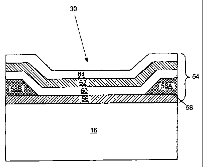
A more detailed illustration of a portion of an ejection head 14 showing an
exemplary heater stack 54 including a heater 30 made according to the above
described
process is illustrated in Fig. 6. The heater stack 54 is provided on an
insulated substrate
16. First layer 56 is the thin film resistor layer made of TaAIN which is
deposited on
the substrate 16 according to the process described above.
After depositing the thin film resistive layer 56, a conductive layer 58 made
of a
conductive metal such as gold, aluminum, copper, and the like is deposited on
the thin
s
CA 02552728 2006-07-05
WO 2005/069947 PCT/US2005/001809
film resistive layer 56. The conductive layer 58 may have any suitable
thickness known
to those skilled in the art, but, in an exemplary embodiment, preferably has a
thickness
ranging from about 0.4 to about 0.6 microns. After deposition of the
conductive layer
58, the conductive layer is etched to provide anode 58A and cathode 58B
contacts to the
resistive layer 56 and to define the heater resistor 30 therebetween the anode
and
cathode 58A and 58B.
A passivation layer or dielectric layer 60 can then be deposited on the heater
resistor 30 and anode and cathode 58A and 58B. The layer 60 may be selected
from
diamond like carbon, doped diamond like carbon, silicon oxide, silicon
oxynitride,
silicon nitride, silicon carbide, and a combination of silicon nitride and
silicon carbide.
In an exemplary embodiment, a particularly preferred layer 60 is diamond like
carbon
having a thickness ranging from about 1000 to about 8000 Angstroms.
When a diamond like carbon material is used as layer 60, an adhesion layer 62
can be deposited on layer 60. The adhesion layer 62 may be selected from
silicon
nitride, tantalum nitride, titanium nitride, tantalum oxide, and the like. In
an exemplary
embodiment, the thickness of the adhesion layer preferably ranges from about
300 to
about 600 Angstroms.
After depositing the adhesion layer 62, in the case of the use of diamond like
carbon as layer 60, a cavitation layer 64 can be deposited and etched to cover
the heater
resistor 30. An exemplary cavitation layer 64 is tantalum having a thickness
ranging
from about from about 1000 to about 6000 Angstroms.
It is desirable to keep the passivation or dielectric layer 60, optional
adhesion
layer 62, and cavitation layer 64 as thin as possible yet provide suitable
protection for
the heater resistor 30 from the corrosive and mechanical damage effects of the
fluid
being ejected. Thin layers 60, 62, and 64 can reduce the overall thickness
dimension of
the heater stack 54 and provide reduced power requirements and increased
efficiency for
the heater resistor 30.
Once the cavitation layer 64 is deposited, this layer 64 and the underlying
layer
or layers 60 and 62 rnay be patterned and etched to provide protection of the
heater
resistor 30. A second dielectric layer made of silicon dioxide can then be
deposited over
the heater stack 54 and other surfaces of the substrate to provide insulation
between
subsequent metal layers that are deposited on the substrate for contact to the
heater
drivers and other devices.
9
CA 02552728 2006-07-05
WO 2005/069947 PCT/US2005/001809
It is contemplated, and will be apparent to those skilled in the art from the
preceding description and the accompanying drawings, that modifications and
changes
may be made in the embodiments of the invention. Accordingly, it is expressly
intended
that the foregoing description and the accompanying drawings are illustrative
of
exemplary embodiments only, not limiting thereto, and that the true spirit and
scope of
the present invention be determined by reference to the appended claims.
to