Note : Les descriptions sont présentées dans la langue officielle dans laquelle elles ont été soumises.
CA 02555573 2006-08-10
WO 2005/077110 PCT/US2005/004507
SILICON NANOTAPER COUPLERS AND MODE-MATCHING DEVICES
Cross-Reference to Related Application
This application claims the benefit of Provisional Application No. 60/543,613,
filed February 11, 2004.
Technical Field
The present invention relates to silicon-based nanotaper couplers and, more
particularly, to nanotaper couplers that may be utilized in conjunction with
free-space
optical couplers to facilitate the coupling of optical signals into and out of
ultrathin,
single-mode silicon waveguides.
Background of the luve>ztio>z
A "nanotaper", or "inverse taper", is generally defined as a terminating
portion of
a core of a high-contrast index waveguide that is used to facilitate efficient
coupling
between a single-mode optical fiber (for example) and an ultrathin, single-
mode high-
contrast index optical waveguide. For the purposes of the present invention,
an
"ultrathin" waveguide is defined as having a typical width on the order of
approximately
0.5 pin and a typical thickness on the order of approximately 0.25 pin. In a
typical
device construction, the lateral dimension of the portion of the nanotaper
proximate to
the core of the high-contrast index waveguide approximately matches the width
of the
core. The lateral dimension of the nanotaper decreases monotonically along the
direction
of light propagation until it reaches a small value associated with a "tip"
(i.e., that
portion of the nanotaper distal from the core of the high-contrast index
waveguide). The
tip portion represents the point at which light first enters the high-contrast
index
waveguide for an "entry" nanotaper, or the point at which light first exits
the high-
contrast index waveguide for an "exit" nanotaper.
In some prior art nanotapers, the device is cleaved such that the tip position
essentially coincides with a cleaved edge. Light is then launched directly
into the tip of
an entry nanotaper, or extracted directly from the tip of an exit nanotaper.
Alternatively,
in other prior art nanotapers, the position of the tip is located inside the
device, away
from the cleaved edge; an auxiliary waveguide is then used to transmit light
from the
cleaved edge to the tip of the nanotaper. The auxiliary waveguide generally
comprises
larger dimensions and a lower refractive index than the ultrathin waveguide,
so that
CA 02555573 2006-08-10
WO 2005/077110 PCT/US2005/004507
maximum coupling efficiency into the optical fiber is achieved since the mode
size and
numerical aperture of the auxiliary waveguide a-re much closer to the fiber
parameters
than the ultrathin waveguide parameters. The care of the auxiliary waveguide
may
comprise a polymer-based material with a refractive index on the order of 1.5 -
1.6.
Other materials, such as silicon oyxnitride, doped silicon dioxide, etc. may
be used to
form the core region of the auxiliary waveguide .
In particular, a prior art nanotaper coupler usually comprises a pair of
waveguide
sections. A first, larger-dimensioned waveguidc section is generally disposed
with
respect to a second, smaller-dimensioned waveguide section such that a portion
of the
first section overlaps a portion of the second section, forming a "mode
conversion
region". One exemplary overlap geometry is disclosed in US Patent Publication
2004/0057667, where FIGS. 1 and 2 illustrate tlLis geometry in a top view and
side view,
respectively. As shown, reference numeral 1 denotes an ultrathin single-mode
waveguide, reference numeral 2 denotes a mode field size conversion region,
reference
numeral 3 denotes an auxiliary waveguide section, and reference numeral 4
denotes a
nanotaper. Within mode field size conversion region 2, nanotaper 4 has a
lateral
dimension that starts at a relatively small value at tip 5 (often 50 - 150
nm), and then
tapers outward to the final desired waveguide dimensions associated with
ultrathin
waveguide section 1. The thickness of nanotapeT 4 remains relatively constant
along
mode field size conversion region 2.
The mode size associated with tip 5 of the nanotaper 4 is "large" (due to the
wcak
confinement of the light) and shrinks as nanotaper 4 expands in size,
providing tighter
confinement of the light as the effective refracti ve index increases along
the length of -the
nanotaper. This effect facilitates the required mode conversion into the
smaller mode
associated with ultrathin single-mode waveguid a 1. As shown, light is
launched into a.n
endface 6 of auxiliary waveguide section 3 (perhaps from an optical fiber -
not shown,
where it propagates along unimpeded until it encounters tip 5 of nanotaper 4
in mode
conversion region 2. At this point, the light bea.in is transferred from the
relatively low
effective index layer 7 of auxiliary waveguide s cction 3 to the relatively
high effective
index ultrathin waveguide 1 with low loss, sincc the mode size is gradually
reduced
along the extent of the taper.
While these and other prior art nanotape r couplers have been successful in
bringing light from an optical fiber into an ultra~hin single-mode waveguide,
there are
limitations in how they may be employed. Perhaps the greatest hindrance in
utilizing the
CA 02555573 2006-08-10
WO 2005/077110 PCT/US2005/004507
prior art nanotaper couplers is the "end fire" coupling requirement; that is,
an optical
fiber (or other waveguide) must provide a signal that couples through a
sidewall
(endface) of an optical substrate and into the nanotaper. Such a coupling
arrangement
requires careful preparation of the sidewall surface in terms of cleaving and
polishing (to
reduce scattering losses), followed by the application of a anti-reflective
(AR) coating.
All of these preparation activities are expensive and time-consuming. A larger
problem
associated with the "end fire" coupling is the fact that only the edge of the
substrate may
be used for coupling; the remainder of the wafer surface is unavailable for
use with a
conventional nanotaper coupler.
Additionally, the larger auxiliary waveguide section often requires the use of
material several microns thick (in order to establish a low-loss interface to
the fiber),
where these dimensions are not compatible with conventional CMOS processing
techniques.
Thus, a need remains in the art for the development of a silicon nanotaper
coupler
that is more robust and can be used as a coupling device at virtually any
location across a
wafer surface.
Summary of the Izzveutiou
The need remaining in the prior art is addressed by the present invention,
which
relates to silicon-based nanotaper couplers and, more particularly, to
nanotaper couplers
that may be utilized in conjunction with free-space optical couplers to
facilitate the
coupling of optical signals into and out of ultrathin, single-mode silicon
waveguides.
In accordance with the present invention, a "nanotaper coupler" refers to a
coupling arrangement that comprises a silicon nanotaper in combination with a
thin
dielectric coupling waveguide having a core refractive index that is greater
than that of
an associated cladding material, but less than the refractive index of
silicon. As before,
the silicon nanotaper is disposed in an overlapping relationship with the
dielectric
waveguide (which serves as the auxiliary waveguide) so as to provide for mode
conversion and coupling of the propagating signal into an associated ultrathin
silicon
waveguide. A free-space coupling device, such as a prism coupler or grating
structure, is
used in accordance with the present invention to couple a free space optical
signal into
the thin dielectric coupling waveguide through the waveguide surface. Thus,
the need
for "end-fire" coupling arrangements, as required in the prior art, is
eliminated.
CA 02555573 2006-08-10
WO 2005/077110 PCT/US2005/004507
Moreover, by using a free-space coupling device (o.g., prism coupler or
grating),
the constraints on the thicknesses and refractive indexes of the materials
comprising the
dielectric waveguide in prior art nanotaper couplers are greatly relaxed. Free-
space
coupling devices couple light efficiently into thin layers of material and can
accommodate a range of refractive index values. Thus, the dimensions of the
dielectric
waveguide can be reduced to values that are compatible with semiconductor
processing
if a suitable high refractive index material is available to comprise the
dielectric
waveguide core. Silicon nitride (n ~ 2) is one exemplary dielectric that may
be used in
implementing the invention.
It is an advantage of the present invention that the utilization of a thin
dielectric
coupling waveguide with a core refractive index less than silicon allows for
various
adjustments to be made in the free-space coupling arrangement to provide for
improved
efficiency. For example, the thickness of the dielectric layer may be
controlled by
conventional CMOS fabrication processes to provide the optimum thickness
required for
coupling (as a function of the specific dielectric material selected).
In a preferred embodiment of the present invention, focusing optics are
included
within the dielectric coupling waveguide to reduce the lateral dimension of
the in-
coupled optical beam as it approaches the entrance of the silicon nanotaper.
The
dielectric coupling waveguide may itself include a tapered profile in the
lateral
dimension to reduce reflections at the interface with the na.notaper.
The utilization of a material other than silicon for the dielectric coupling
waveguide allows for materials other than silicon to also b a used to form the
associated
free-space optical coupler, providing for some relaxation on the geometry of
the launch
conditions required for coupling a light beam into and out of a surface
waveguide layer.
It is an aspect of the present invention that the dielectric coupling
waveguide in
conjunction with a silicon nanotaper may be used to provide coupling into and
out of
ultrathin silicon waveguides at any location on an opto-electronic structure
(not limited,
that is, for use as an input/output coupler). In this case, the dielectric
coupling
waveguide can be used to form various optical devices (pa..ssive devices) that
are not
compatible with the properties of ultrathin waveguides (scattering loss
problems, for
example), reserving the use of the ultrathin waveguides for high-performance
active
optical devices.
CA 02555573 2006-08-10
WO 2005/077110 PCT/US2005/004507
Other and further embodiments and aspects of the present ir3~vention will
become
apparent during the course of the following discussion, and by reference to
the
accompanying drawings.
5 Brief Description of the Drawings
Referring now to the drawings,
FIGS. 1 and 2 illustrate an exemplary prior art nanotaper coupling
arrangement;
FIG. 3 contains a side view of an SOI-based exemplary hybrid coupler formed in
accordance with the present invention;
FIG. 4 contains a top view of an SOI-based exemplary hybrid coupler formed in
accordance with the present invention;
FIG. 5 contain plots illustrating the wavelength dependence associated with
8s;,
the beam angle inside an exemplary prism coupler;
FIG. 6 contains plots illustrating the wavelength dependence associated with
Aa;r,
the beam launch angle into an exemplary prism coupler;
FIG. 7 contains a top view of one exemplary arrangement ru'here focusing
optics
is included in the inventive arrangement;
FIG. 8 illustrates, in a top view, an alternative embodiment of the present
invention, incorporating passive optics into the dielectric waveguide layer;
FIG. 9 is a side view of the arrangement illustrated in FIG. S;
FIG. 10 is a top view of an alternative arrangement for including passive
optics in
the arrangement of the present invention;
FIG. 11 illustrates an arrangement including both an input coupler and output
coupler, in this case a trapezoidal prism coupler, formed in accordance with
the present°
invention;
FIG. 12 is a top view of an exemplary out-coupling arrangement for use in the
structure of FIG. 1 l;
FIG. 13 illustrates an alternative embodiment of the present invention, using
a
grating as a free-space optical coupling arrangement; and
FIG. 14 is a top view of the embodiment of FIG. 13.
CA 02555573 2006-08-10
WO 2005/077110 PCT/US2005/004507
Detailed Description
The utilization of a hybrid coupling arrangement comprising a silicon-based
nanotaper coupler and free-space optical coupler, in accordance with the
present
invention, addresses many of the problems associated with the prior art end-
fire couplers
and offers additional flexibility with respect to wafer-scale fabrication and
free-space
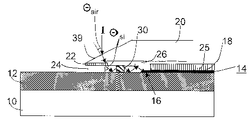
optical coupling. FIG. 3 contains a side view, and FIG. 4 a top view, of an
SOI-based
exemplary hybrid coupler formed in accordance with the present invention. In
most
cases, the devices formed in accordance with the present invention will
comprise an SOI
structure including a silicon substrate 10, a silicon dioxide insulating layer
12 and an
upper silicon device layer (hereinafter referred to as an "SOI layer") 14,
where SOI layer
14 generally comprises a thickness of less than one micron.
A silicon nanotaper 16 (best illustrated in FIG. 4) is formed within a portion
of
SOI layer 14 and used, as discussed above, to provide efficient coupling into
an ultrathin
silicon strip waveguide 18 also formed within SOI layer 14. In accordance with
the
present invention, various limitations associated with prior art end-fire
nanotaper
coupling arrangements are overcome by including a free-space optical coupling
element
with the SOI-based structure. In the exemplary embodiment as illustrated in
FIGS. 3 and
4, a prism coupler 20 and associated evanescent coupling layer 22 are used to
couple a
free-space optical beam into a dielectric waveguide coupling layer 24, with
light
propagating in dielectric waveguide 24 until it reaches silicon nanotaper 16,
where the
light is then transferred to ultrathin silicon waveguide 18. Alternatively, as
discussed in
further detail below, a grating structure may be used as a free-space optical
coupler to
guide a propagating optical signal into dielectric waveguide coupling layer
24.
In accordance with the present invention, relatively thin dielectric coupling
layer
24 is included in the inventive arrangement and used to couple the incoming
light I from
prism coupler 20 into silicon nanotaper 16, where the refractive index of
layer 24 is
selected to be greater than that of evanescent coupling layer 22 and
insulating layer 12,
yet less than that of silicon. In one embodiment, silicon dioxide (n=1.45) may
be used to
form evanescent coupling layer 22 (as well as insulating layer 12). In this
case, silicon
nitride (n approximately 2) may be used to form dielectric coupling layer 24,
where
silicon nitride is a common material used in CMOS processing and can easily be
deposited, patterned and etched to exhibit the desired dimensions.
In order to provide the desired light coupling into nanotaper 16, an end
portion of
dielectric coupling layer 24 is disposed to overlap a predetermined terminal
portion of
CA 02555573 2006-08-10
WO 2005/077110 PCT/US2005/004507
nanotaper 16 within a mode field size conversion section 26. Preferably,
dielectric
coupling layer 24 is formed to include a tapered profile in the lateral
direction as it nears
nanotaper 16 (illustrated by reference numeral 28 in FIG. 4) so as to reduce
reflection
losses at the interface between dielectric coupling layer 24 and an upper
cladding layer
25 of the silicon strip waveguide (shown in FIG. 3). As will be described in
detail
hereinbelow, a focusing element 30 is formed within dielectric coupling layer
24 and
used to facilitate the focusing of the incoming beam into the spot size
appropriate for
nanotaper 16. Focusing element 30 may take the form of a lens, a mirror or an
adiabatic
coupling arrangement to form a mode-preserving coupler.
In operation, an incoming free-space optical signal I impinges on an input
facet
39 of prism coupler 20, and then passes through evanescent coupling layer 22
to be
coupled into a slab mode of dielectric coupling layer 24. The outline of the
propagating
optical beam B is illustrated in FIG. 4. Advantageously, the use of such a
coupling
arrangement allows for the beam to enter a wafer surface at virtually any
desired
location, as long as a prism coupler (or other free-space optical coupling
device) and
evanescent coupling region are present. Additionally, the use of a dielectric
coupling
layer 24 (such as silicon nitride) reduces past limitations associated with
the use o f a
silicon material (in particular, SOI layer 14) as this coupling element.
Moreover, -the use
of an alternative material for this dielectric coupling layer opens up many
other m aterials
options for prism coupler 20.
Indeed, an advantage of utilizing a separate dielectric coupling layer 24 in
place
of SOI layer 14 in the input coupling region is that the refractive index of
this input
coupling region can now be modified as need be. In most cases in the prior
art, SOI
layer 14 is utilized to not only to couple into the SOI structure, but to form
other
components within the opto-electronic system. These additional requirements of
the SOI
layer controls both the doping and thickness of SOI layer 14 for both optical
and
electrical considerations, thus not allowing the parameters of the SOI layer
14 to be
modified for optimum coupling performance. This constraint, in turn, places
significant
constraints on the geometry of the launch conditions for the input (as well as
output)
beam.
Therefore, by virtue of processing SOI layer 14 to eliminate a portion of the
layer
and replace it with the dielectric waveguide coupling material such as silicon
nitri de, the
thickness of this deposited silicon nitride layer may be controlled (using
standard CMOS
processes) so that the final dielectric region exhibits the precise dimensions
required for
CA 02555573 2006-08-10
WO 2005/077110 PCT/US2005/004507
efficient optical coupling. In one embodiment, the thickness of dielectric
coupling layer
24 may be less than 0.5 p,m, with insulating layer 12 having a thickness on
the order of
1.0 p.m.
In prior arrangements, where a silicon waveguiding region (usually, the SOI
layer) was utilized to couple a free space beam into an SOI structure, the
associated
prism coupler was also formed, of necessity, from silicon. Now, with the use
of a
different dielectric material for the waveguiding coupling region (with a
lower refractive
index than silicon), many other materials and/or arrangements may be used to
form the
prism coupler. The ability to select a different material is also considered
to somewhat
"relax" the stringent requirements on the input beam coupling angle (with
respect to
input facet 32), the thickness/properties of evanescent coupling layer 22,
etc.
An additional advantage is found by using silicon nitride in place of silicon
as the
coupling waveguide. Indeed, when using silicon nitride, the light launch
condition has
been found to be less sensitive to wavelength, allowing for the inventive
coupling
arrangement to be used over a broader wavelength range. FIGs. 5 and 6 contain
plots
illustrating this aspect of the present invention for Os; (the beam angle
inside prism 20 -
see FIG. 3) arid Oa;r (the beam launch angle into prism 20 - see FIG. 3),
respectively.
Referring to FIG. 5, a comparison between using a silicon nitride waveguide
coupling
layer to a prior art silicon coupling layer is shown. As is obvious from the
results, there
is very little change in the optimum value for Os; as the input wavelength is
varied over
the range of 1.3 - 1.65 ~.m when using a silicon nitride coupling waveguide -
allowing a
single device to efficiently coupling multiple wavelengths (especially useful
in WDM
applications). In contrast, the prior art arrangement shows a variation of
more than 5°
over this same wavelength range. A similar result is illustrated in the graph
of FIG. 6,
where the prior art change in 6a;r is shown as varying from less than
20° to almost 40°
over the wavelength range of interest. When using a silicon nitride coupling
waveguide,
in accordance with the present invention, this angle dependence is reduced to
a value of
no more than 5° over the same bandwidth.
In order to prevent having optical signal loss through light "leaking" from
dielectric coupling layer 24 into underlying dielectric layer 12 and substrate
10, tight
confinement of the optical signal within dielectric coupling layer 24 is
required.
Therefore; the refractive index of dielectric coupling layer 24 must
significantly exceed
that of a standard cladding material (e.g., silicon dioxide with n=1.45). As
mentioned
CA 02555573 2006-08-10
WO 2005/077110 PCT/US2005/004507
above, silicon nitride, with a refractive index of approximately 2, is an
exemplary
relatively high refractive index material that can be used for this purpose.
Other
materials, such as a doped silicon dioxide, silicon oxynitride and silicon
carbide may also
be used.
While the effective thickness of dielectric coupling layer 24 is typically
less than
one micron, the beam diameter (as shown by the optical mode profile O) may be
on the
order of tens of microns. In order to provide efficient coupling of the beam
into the
ultrathin silicon waveguide (on the order of one micron, or less), the lateral
dimension of
the beam needs to be reduced to that of the waveguide. Using a prior art
nanotaper
arrangement to provide the desired coupling power would require the nanotaper
to have a
length inappropriate for use in SOI-based opto-electronic devices, where space
comes at
a premium. Therefore, additional focusing optics 30 are used in the inventive
arrangement, disposed along dielectric coupling layer 24, to reduce the
lateral dimension
of the optical mode O prior to the beam entering mode conversion region 26
defined by
the overlap of dielectric coupling layer 24 and nanotaper 16. It is to be
understood that
various other arrangements may be used to provide the desired lateral
confinement. For
example, a photonic bandgap (PBG) structure may also be formed along a portion
of
dielectric coupling layer 24 and provide the desired confinement at the
interface with
mode conversion region 26. An adiabatically tapered structure may also be
used.
Various types of focusing arrangements can be used to provide the desired beam
shaping in the mode conversion region. FIG. 7 contains a top view of one
exemplary
arrangement where focusing optics 30 is shown as comprising a turning mirror
32 and a
focusing mirror 34, disposed as shown along the beam path within dielectric
coupling
layer 24. Advantageously, these waveguide mirrors may be easily formed in
dielectric
coupling layer 24 utilizing conventional CMOS fabrication techniques. In the
case
where dielectric coupling layer 24 comprises a layer of silicon nitride,
turning mirror 32
and focusing mirror 34 may comprise silicon dioxide. As a result of the
difference in
refractive index between these two materials, essentially all of the impinging
light beam
will be reflected off of the encountered surfaces. Therefore, the propagating
optical
signal will first reflect off of surface 36 of turning mirror 32 and be
directed to surface 38
of focusing mirror 34. The focusing provided by focusing mirror 34, as shown
in FIG.
7, results in significantly reducing the lateral dimension of the beam as it
enters mode
conversion region 26, and ultimately into nanotaper 16.
CA 02555573 2006-08-10
WO 2005/077110 PCT/US2005/004507
In an alternative embodiment (not shown), a convex waveguide lens can be
fabricated within dielectric coupling layer 24. In this case, dielectric
coupling slab layer
24 may comprise silicon nitride, while the lens element is formed of an oxide
material.
It is well-known that the narrow, ultrathin silicon waveguides also referred
to as
"silicon wires") have exceedingly small dimensions, on the order of 0_2~,m x
O.S~m and
tend to be somewhat lossier than their dielectric counterparts. The increased
optical loss
can be attributed to factors such as the high index contrast, sidewall
roughness, doping
requirements, etc. For very low loss applications, or applications that
require long
optical path lengths to increase device sensitivity (such as sensors, for
example), the loss
10 associated with a silicon wire waveguide is prohibitively high. Thus, in
accordance with
the teachings of the present invention, the combination of a dielectric
coupling layer 24
with a silicon nanotaper 16 can be used to intentionally locate various
optical devices
within either dielectric coupling layer 24 or silicon wire 18. Indeed, a
number of passive
optical devices (such as, for example, lenses, mirrors, filters, gratings,
etc.) may be
formed within dielectric coupling layer 24, since layer 24 exhibits larger
dimensions
(with less loss), allowing for relatively long waveguide path lengths to be
used. Silicon
wire 18 may be "saved", therefore, for use with only the critical active
optical devices.
FIG. 8 contains a top view of an exemplary arrangement for incorporating a
plurality of passive optical devices 40 into dielectric coupling layer 24~
with a partial side
view (without the associated coupling optics) in FIG. 9. The specific number
and types)
of passive optical devices are not shown in FIGs. 8 and 9. An alternative
embodiment is
illustrated (in a top view) in FIG. 10, where turning mirror 32 and focusing
mirror 34 are
disposed at the output of the plurality of optical devices 40, so as to focus
the output
from focusing mirror 34 directly into mode conversion region 26:
Indeed, this specific aspect of the present invention may be implemented at
various locations within an SOI structure and need not be associated with the
activities of
coupling light into and out of the SOI layer itself. That is, a combination of
dielectric
coupling layer 24 and nanotaper 16 may be judiciously used at various
locations where
both passive and active optical structures are required, with the passive
devices formed
in dielectric coupling layer 24, and nanotaper 16 used to efficiently couple
the light from
the passive components into one or more active devices formed in silicon wire
18. A
similar taper can then be used, transfer the light energy from a silicon wire
back into
another dielectric waveguide.
CA 02555573 2006-08-10
WO 2005/077110 PCT/US2005/004507
11
As mentioned above, the hybrid free-space/nanotaper coupling arrangement of
the present invention is equally applicable to improve the out-coupling from
ultrathin
silicon waveguide region through a coupler and back into free space. FIG. 11
illustrates
an arrangement including both an input coupler and output coupler, in this
case a
trapezoidal prism coupler 50. Referring to FIG. 11, trapezoidal prism coupler
50 is
illustrated as including an input facet 52 and an output facet 54 (with an
input beam "I"
shown as impinging input facet 52, and an output beam "O" shown as exiting
along
output facet 54).
As described above, input beam I will propagate through prism coupler 50 and
then enter evanescent coupling layer 22 (where evanescent coupling layer 22
generally
comprises silicon dioxide). The optical beam is thereafter coupled into
dielectric
coupling layer 24 (formed of an appropriate thickness), where the signal then
encounters
passive optical devices including at least focusing optics 30 and, possibly a
plurality of
passive optical devices 40. Mode conversion region 26 defines the overlap
between
dielectric coupling layer 24 and nanotaper 16. As shown, the optical signal
will go
through a mode conversion, propagate along nanotaper 16 and ultimately be
coupled into
ultrathin ("silicon wire") waveguide 18. Clearly shown in the embodiment of
FIG. 11 is
the location of upper cladding layer 25 (usually comprising silicon dioxide)
with respect
to ultrathin waveguide 18, which in combination with dielectric layer lower
cladding
layer 12 will confine the propagating optical signal within ultrathin
waveguide 18.
A second silicon nanotaper 56, also referred to as "exit" nanotaper, is
illustrated
in FIG. 11 as disposed at the termination of ultrathin waveguide 18. In this
case, the
lateral dimension of exit nanotaper 56 is shown as narrowing as it nears
output coupling
facet 54. This aspect is best illustrated in FIG. 12. A dielectric coupling
waveguide 58
is illustrated in FIGS. 11 and 12 as disposed so as to overlap the terminal
portion of exit
nanotaper 56 to form a mode conversion region 57 and allow the propagating
signal to
expand into dielectric coupling waveguide 58. Passive optical devices 60 are
illustrated
as formed within dielectric coupling waveguide 58 including, at the least, a
collimating
mirror (not shown) to properly redirect the propagating signal into an exit
evanescent
coupling layer 62, through coupling prism 50 and exiting through output facet
54.
While the above-described embodiments of the coupling aspect of the present
invention utilized a prism coupler to bring a free-space optical signal into
the SOI layer
(and also launch a surface-propagating beam back into free space), various
other free
space coupling arrangements may be utilized in conjunction with the dielectric
CA 02555573 2006-08-10
WO 2005/077110 PCT/US2005/004507
12
waveguide/nanotaper arrangement of the present invention. FIGS. 13 and 14
illustrate
one specific alternative, utilizing a grating structure 70 instead of prism
coupler 20 (or
50). FIG. 13 contains a side view and FIG. 14 a top view of this particular
embodiment.
As shown, a grating 70 is formed in evanescent coupling layer 22. (and/or
possibly
dielectric layer 24) to couple free-space optical signal I into dielectric
coupling layer 24.
In this case, the period of grating 70 (denoted "A" in FIGS. 13 and 14) is
determined, in
conjunction with the properties of dielectric coupling waveguide 24, to
provide the most
efficient coupling arrangement. It is an advantage of the arrangement of the
present
invention that the properties of dielectric coupling waveguide 24 can be
adjusted during
fabrication (e.g., including of dopants during fabrication, control of
thickness, etc.) so
that such a grating will provide a sufficient amount of coupling. Although not
illustrated
specifically in FIGs. 13 and 14, it is obvious that a similar arrangement may
be used as
an output coupler, as discussed above in association with FIGS. 1 1 and 12.
From the invention thus described, it will be obvious that -the embodiments of
the
invention may be varied in many ways. Such variations are not to be regarded
as a
departure from the spirit and scope of the invention, and all such
modifications as would
be obvious to one skilled in the art are intended for inclusion within the
scope of the
invention as defined by the following claims.