Note : Les descriptions sont présentées dans la langue officielle dans laquelle elles ont été soumises.
CA 02556117 2006-08-14
Docket No. 52388
BONDING METHODS AND OPTICAL ASSEMBLIES
This application claims the benefit of priority under 35 U.S.C. ~ 119(e) to
U.S.
Provisional Application No. 60/708,552, filed August 15, 2005, the entire
contents of
which are incorporated herein by reference.
The present invention relates generally to the field of bonding and more
specifically to the field of optoelectronics. In particular, the present
invention relates to
methods of bonding two objects together, for example, bonding components such
as
lenses, optical fibers and hermetic lids in optical assemblies. As well, the
invention
relates to optical assemblies which include bonded components. The invention
fords
particular applicability to the manufacture of micro-optical assemblies.
Optical assemblies include optical components such as lenses, etalons, and
optical
fibers, and may include additional components, for example, optoelectronic
devices such
as semiconductor laser die and photodiodes, as well as lids for hermetically
sealing the
components. The assemblies further include substrates, or submounts, to which
the
1 S components are bonded. The bonding agents used are selected based, for
example, on
component and substrate material, and desired bonding temperature. Bonding
agents
containing organic materials such as epoxies are known. Organic materials,
however, act
as contaminants with respect to optical and optoelectronic components,
adversely
affecting reliability of the formed assemblies. It would therefore be desired
to avoid
organic-containing bonding agents, particularly in hermetically sealed optical
assemblies.
In the optical assembly manufacturing process, the components are typically
bonded to the substrate in a sequential manner at progressively lower
temperatures to
prevent movement or detachment of a previously bonded component due to
loosening of
the bonding joint. A typical bonding material for optoelectronic devices is a
high-
temperature solder such as Au/Sn (80:20 eutectic) which has a melting
temperature of
about 280°C. When bonding components after the optoelectronic device,
bonding
temperatures should be less than the melting point of such solder to avoid re-
melting of
the Au/Sn solder joint.
Optical components, such as optical fibers, lenses, filters and etalons, are
typically
formed of glass or contain a glass-like optical coating. One technique for
soldering such
-1-
CA 02556117 2006-08-14
Docket No. 52388
components to the substrate involves coating a portion of the optical
component with a
metal which is adherent to the solder. This technique, however, adds
complexity and cost
to manufacture of the optical assemblies.
U.S. Patent No. 5,178,319 discloses methods for bonding optical elements such
as
glass spheres and optical fibers to aluminum. The disclosed methods involve
applying
pressure together with energy in the form of heat and/or acoustic energy to
the interface
of the optical element and the aluminum. For purposes of applying heat to the
interface,
the '319 patent discloses a temperature greater than 300°C, such as
350°C. To allow for
a more flexible bonding hierarchy, methods allowing for bonding of optical
components
at lower temperatures than those used with aluminum would be desirable.
The present invention addresses one or more of the foregoing problems
associated
with the state of the art.
A first aspect of the invention provides methods of bonding a first object to
a
second object. The methods involve: (a) providing a first object; (b)
providing a second
object; and (c) chemically bonding the first object to the second object with
a bonding
agent that includes magnesium.
A second aspect of the invention provides methods of bonding a component in an
optical assembly. The methods involve: (a) providing a substrate; (b)
providing a
component to be bonded to the substrate; and (c) chemically bonding the
component to
the substrate with a bonding agent that includes magnesium.
In a third aspect of the invention, optical assemblies are provided. The
optical
assemblies include a substrate, a component, and a bonding agent that includes
magnesium between the substrate and the component for chemically bonding the
component to the substrate.
In the methods and optical assemblies of the invention, component such as
lenses,
optical fibers and hermetic lids can easily be bonded to a substrate. A useful
substrate
material is silicon, such as single-crystal silicon which may conveniently be
in wafer
form and which can be made to have a surface oxide. The bonding material may
take the
form, for example, of one or more preforms, or a layer coated on the optical
component
and/or substrate. The technique for bonding the component to the substrate may
be, for
example, a thermo-compression process. The methods may be used in the
manufacture
-2-
CA 02556117 2006-08-14
Docket No. 52388
of hermetically sealed devices, for example, a hermetically sealed
optoelectronic micro-
component which includes an optoelectronic device and optical component
disposed in a
hermetically sealed volume.
As used herein, the terms "a" and "an" are inclusive of "one or more". The
term
"on" and "over" are used interchangeably in defining spatial relationships,
and
encompass the presence or absence of intervening layers or structures. Also as
used
herein, the term "optical assembly" encompasses structures having optical
functionality
with or without optoelectronic functionality. Also as used herein, the term
"metal"
encompasses pure metals, metal alloys and metal composites.
The present invention will be discussed with reference to the following
drawings,
in which like reference numerals denote like features, and in which:
FIG. 1 illustrates an exemplary optical assembly in accordance with the
invention;
FIGS. 2A-B illustrate the bonding of components in the optical assembly of
FIG.
1, in accordance with the invention; and
FIG. 3 illustrates exemplary bonding pellets or preforms which may be used in
the
methods of the invention.
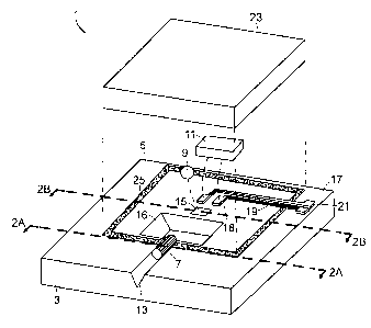
The present invention will now be described with reference to FIG. 1,
depicting
an illustrative optical assembly 1 in which the bonding methods of the present
invention
find application. The optical assembly includes a substrate 3 having an upper
surface 5 in
and on which various surface features are formed. The substrate 3 is typically
formed
from a semiconductor material which may be in wafer or chip form, such as
silicon, for
example, <100> single-crystal-silicon, gallium arsenide, indium phosphide, or
lithium
niobate, ceramic, polymer, or metal. Various components may be bonded to the
substrate
upper surface 5, including optical and optoelectronic components, as well as a
lid for
hermetically sealing the assembly. Typical optical components include, for
example,
optical fibers, lenses, filters and etalons. Optoelectronic devices include,
for example,
laser die and photodetectors. In the illustrated embodiment, an optical fiber
stub 7, ball
lens 9, and optoelectronic device 11 are bonded to the substrate upper surface
5.
The upper surface 5 includes one or more surface features formed therein or on
for holding the various components. The illustrated surface features include a
groove 13,
such as a V-groove (shown) or U-groove, for holding the optical fiber stub 7,
pit 15 for
-3-
CA 02556117 2006-08-14
Docket No. 52388
holding the ball lens 9, light clearance pit 16, and metal feature 17 for
electrical
connection of the optoelectronic device 11. Metal feature 17 includes contact
pads 18 to
which optoelectronic device 11 is soldered, metal lines 19 and bonding pads 21
for
connection to a power supply. Techniques for forming the surface features are
known to
those skilled in the art. For example, the V-groove and lens and light
clearance pits may
be formed using masking and wet and/or dry etching techniques, while the
metallization
structure may be formed by sputtering, evaporation or plating techniques.
These
techniques may optionally be used to form a substrate master from which
substrates may
be formed in a molding process. A lid 23 may further be provided for forming a
hermetically enclosed volume for housing the optical and optoelectronic
components.
FIGS. 2A and 2B illustrate in cross-section along lines A-A and B-B of FIG. 1,
optical fiber stub 7 and ball lens 9, respectively, in the process of being
bonded to
substrate 3. The optical component is typically formed of an oxide material,
for example,
a doped glass, such as a borosilicate glass, for example, BK7 borosilicate
glass,
1 S commercialliy available from Schott Glass Technologies Inc., Duryea, PA
USA, a
ceramic such as alumina, or a crystal such as sapphire, spinel, or cubic
zirconia. If the
optical component is not formed of an oxide, it may be coated with an oxide
layer such as
stoichiometric (Si02) or non-stoichiometric silicon oxide, tantalum oxide, or
titanium
oxide, to allow bonding with the bonding agent, described below.
Bonding of components such as optical components 7, 9 and the hermetic lid 23
to the substrate is facilitated with a bonding agent 25. The bonding agent
includes
magnesium and is typically magnesium-based (greater than 50 wt% magnesium
based on
the total bonding agent), for example, metallic magnesium (>99 wt% Mg), a
magnesium-
based alloy or a magnesium-based composite. Typically, the bonding agent is
metallic
magnesium. A magnesium-based alloy or composite may be useful, for example, to
modify one or more properties of the bonding agent, such as bonding
temperature,
corrosion resistance, and bond strength. Suitable alloying agents include, for
example,
Al, Si, Sn, Zn, Zr, Pb, as well as the rare earth elements. Suitable
composites include, for
example, AZ61A-F (92.35 wt% Mg, 6.5 wt% Al, 0.15 wt% Mn, 1.0 wt% Zn), AZ10A-F
(98.2 wt% Mg, 1.2 wt% Al, 0.2 wt% Mn, 0.4 wt% Zn) and AM20-F (97.8 wt% Mg, 2.1
-4-
CA 02556117 2006-08-14
Docket No. 52388
wt% Al, 0.1 wt% Mn), as denoted by the American Society for Testing and
Materials
(ASTM).
The bonding agent may take the form of a coating formed on the surface of the
substrate and/or the component, for example, by evaporation, electroless
plating,
S electrolytic plating, sputtering or other known metallization technique. An
intermediate
layer may optionally be used to increase adhesion, provide a seed layer for
plating or to
act as an insulator, for example, between metal lines 19 beneath the bonding
agent. The
bonding agent thickness to be used will depend, for example, on the bonding
agent
material, bonding agent density, bonding temperature, geometry of the optical
component
and that of the bonding region of the substrate. The film density will also
play a role in
determining the ideal layer thickness. A typical prebonded thickness for a
metallic
magnesium layer is from 2 to 25 Vim, for example, from 10 to 15 pm.
The bonding agent may optionally take the form of one or more pellets or
preforms 27 as illustrated in FIG. 3. In this exemplified method, the pellets
or preforms
may be placed in the recess (e.g., groove 13 or lens pit 15) in the substrate
surface prior
to or after introducing the optical component into the recess. The use of
pellets and
preforms in this manner effectively eliminates the expense, processing time
and
complexity associated with metallization processes. In addition, the pellets
and preforms
may each be formed from a precise amount of bonding agent and thus produce
consistent
and uniform bonding. Typically, pellets are generally spherical in geometry
but may be
irregularly shaped. Preforms may be of any geometry, for example, spherical,
torroidal,
ellipsoidal or cylindrical. Magnesium preforms are commercially available, for
example,
from Read International, Riverside, RI USA. In the case of a spherical pellet
or preform,
for example, a typical size is from 50 to 300 ~,m, for example, about 100 ~,m,
for bonding
a 400 pm ball lens or a 125 ~m fiber stub. Suitable geometry and size of the
pellets and
preforms will depend on various factors, such as geometries of the component
and
substrate to be bonded.
The bonding agent does not bond well to certain substrate materials, for
example,
silicon and gallium arsenide. In such case, one or more layers 28 of a
material to which
the bonding agent will bond may be formed on the substrate. For example, this
layer may
be formed on the substrate upper surface or on surface features, for example,
on the
-5-
CA 02556117 2006-08-14
Docket No. 52388
bonding surface of the groove 13 and lens pit 15. Suitable layers include, for
example, an
oxide such as a silicon oxide such as stoichiometric (Si02) or non-
stoichiometric silicon
oxide, or a metal layer, for example, a layer of aluminum. Suitable
thicknesses for these
layers will depend, for example, on the specific materials involved and would
be
understood by those skilled in the art.
The components may be bonded to the substrate 3 with the bonding agent 25
using a thermo-compression bonding technique. In such a process, pressure is
applied
between the optical component and substrate to compress the component against
the
substrate as shown by the arrows in FIGS. 2A-B. The thermo-compression bonding
technique additionally involves heating of the bonding agent such that the
bonding agent
is at an elevated temperature during the pressure application. The bonding
agent may be
heated prior to and/or at the same time the component is compressed against
the
substrate. In addition, it may be beneficial to continue heating the assembly
for a period
following the compression. Without being bound by any particular theory, it is
believed
that the pressure applied between the component and the substrate causes the
component
to penetrate native oxide formed on the bonding agent. The magnesium in the
bonding
agent directly contacts and reacts with the oxide or oxide coating of the
component,
forming an oxide-magnesium bond. The magnesium in the bonding agent thus forms
the
primary constituent of the chemical bond.
The temperature and pressure applied in the bonding process are high enough to
cause bonding between the component and substrate but less than that which
would cause
deformation or otherwise damage the component. The temperature and pressure
will
depend, for example, on the bonding agent material, as well as the material
and
geometries of the component and substrate (e.g., bonding area) and any
intervening
layers. The bonding temperature is typically from 225 to 500°C, for
example, from 250
to 300°C, and may be less than 300°C. The following examples are
intended to illustrate
further various aspects of the present invention, but are not intended to
limit the scope of
the invention in any aspect.
-6-
CA 02556117 2006-08-14
Docket No. 52388
FXAMPT FC
Example 1
With reference to FIGS. 2A-B, a 125 pm diameter glass optical fiber stub 7 and
a
400 pm diameter spinel ball lens coated with 1026 silicon nitride and 2505
silicon
dioxide are bonded to a <100> silicon substrate 3 as follows. A V-groove 13
(nominally
133 ~m width) and lens pit 15 (470 by 470 ~m width at the substrate surface,
270 pm
depth) are formed in the upper surface of the silicon substrate by anisotropic
wet etching.
A 4700 thick silicon dioxide layer is formed on the surface of the substrate,
V-groove
and pit by thermal oxidation. A 12 ~m thick layer of magnesium is formed over
the
oxide in the V-groove and lens pit by thermal evaporation. The fiber stub and
ball lens
are placed in the V-groove and pit, respectively, and the structure is heated
to 275°C on a
hot plate. The fiber stub contacts the bonding agent-coated V-groove at two
points along
its length while the ball lens contacts the pit at four points. Pressure in an
amount of 800
grams/mm is applied along the length of the fiber stub and 1000 grams to the
ball lens for
10 seconds. The pressure is applied with a pneumatic piston connected to a
steel rod
which contacts the fiber stub and ball lens. The temperature is maintained
during
pressure application and for 50 additional seconds. Thermo-compression bonds
between
the substrate and both the fiber stub and ball lens are thus formed.
Example 2
The procedures and materials of Example 1 are repeated, except in place of the
magnesium layer, two 50-75 ~m diameter spherical magnesium pellets are
disposed in
the V-groove and one such pellet is disposed in the lens pit.
Example 3
The procedures and materials of Example 2 are repeated, except the magnesium
pellets are each replaced with a 100 Etm long by 125 pm diameter cylinder of
ASTM
AZ61A (92.35 wt% Mg, 6.5 wt% Al, 0.15 wt% Mn, 1.0 wt% Zn) wire.
_7_