Note : Les descriptions sont présentées dans la langue officielle dans laquelle elles ont été soumises.
CA 02559780 2006-09-13
WO 2005/088830 PCT/GB2005/000942
-1-
A Doherty Amplifier
The present invention relates to a Doherty amplifier. More particularly, but
not exclusively,
the present invention relates to a Doherty amplifier having reduced inter-
stage reflection
ripple within the amplifier.
Background
In the 1930s a high efficiency, linear, valve based power amplifier was
devised by
W. H. Doherty. This 'Doherty' amplifier configuration consisted of two valve
amplifiers,
namely the main amplifier and the auxiliary amplifiers, which delivered power
into a common
load in a very efficient manner. More recently, the Doherty amplifier has been
realised with
to semiconductor transistor amplifiers replacing the valve amplifiers.
Amplifier efficiency rl is the proportion of the DC power PDC supplied to the
amplifier
network relative to the available RF power P~ at the output of the amplifier
network that is
then delivered to the load. Le. r) = P~./PDC.
One problem associated with the Doherty design is the sensitivity to operating
frequency. The
individual amplifiers within the Doherty amplifier have input and output
matches which alter
with varying power level. This variation generates mismatches. These
mismatches cause
ripple within the transmission path of the amplifier and reduce the frequency
flatness of the
design.
The standard Doherty amplifier is more efficient than a conventional amplifier
but can be
difficult to optimise.
The present invention comprises a Doherty amplifier comprising:
a power splitter having a first output and a second output, wherein
the first output is connected to a main power splitter having first and second
outputs
which differ in phase by 90°; and
CA 02559780 2006-09-13
WO 2005/088830 PCT/GB2005/000942
the second output is connected to an auxiliary power splitter having first and
second
outputs which differ in phase by 90°;
a main final stage amplifier comprising first and second main paired
amplifiers, the
inputs of which are connected to the first and second outputs of the main
power splitter;
an auxiliary final stage amplifier comprising first and second auxiliary
paired
amplifiers, the inputs of which are connected to the first and second outputs
of the auxiliary
power splitter; wherein
the output from the first main paired amplifier is connected to the output
from the
first auxiliary paired amplifier by an impedance inverter; and
i o the output from the second main paired amplifier is connected to the
output from the
second auxiliary paired amplifier by an impedance inverter;
the amplifier being arranged such that a relative phase shift is introduced to
the
signals input to the main and auxiliary power splitters to offset the phase
shift of the
impedance inverters.
15 The Doherty amplifier of the invention has the advantage of improved
frequency flatness and
stability.
Preferably, the amplifier ftuther comprises:
a main driver amplifier connected between the first output of the power
splitter and
the input of the main power sputter; and
2o an auxiliary driver amplifier connected between the second output of the
power
splitter and the input of the auxiliary power sputter.
Preferably, the phase of the second outputs of the main and auxiliary power
splitters lead the
phases of the corresponding first outputs of these splitters.
Preferably, the phases of the second outputs of the main and auxiliary power
splitters lag
25 behind the phases of the corresponding first outputs of these splitters.
Preferably, the power splitter introduces a phase shift between the first and
second outputs to
offset the phase shift of the impedance inverters.
CA 02559780 2006-09-13
WO 2005/088830 PCT/GB2005/000942
-3-
Preferably, at least one of the main driver amplifier and auxiliary driver
amplifier introduce a
relative phase shift to the input of the corresponding main or auxiliary power
splitter to offset
the shift of the impedance inverters.
Preferably, the Doherty amplifier further comprises a combiner having a first
input port
connected to the output of the first auxiliary amplifier and a second input
port connected to
the output of the second auxiliary amplifier,
the combiner being adapted to introduce a phase change between the signals
received
at the first and second input ports opposite to the phase change introduced by
the auxiliary
power splitter and to combine these two signals at an output port.
to More preferably, the phase change is 90°.
The Doherty amplifier can comprise a load connected to the output of the
combiner via a
further impedance transformer. The load can then terminate differential
signals.
Alternatively, the Doherty amplifier can further comprise:
a load connected to the output of the combiner;
a first combiner impedance transformer connected between the first auxiliary
amplifier and the first input port of the combiner; and
a second combiner impedance transformer connected between the second auxiliary
amplifier and the second input port of the combiner.
At least one of the main driver amplifier and auxiliary driver amplifier can
be single ended.
2o At least one of the main driver amplifier and auxiliary driver amplifier
can comprise a pair of
balanced amplifiers.
The Doherty amplifier can comprise a plurality of main driver amplifiers
connected in cascade
before the main power splitter.
CA 02559780 2006-09-13
WO 2005/088830 PCT/GB2005/000942
-4-
The Doherty amplifier can comprise a plurality of auxiliary driver amplifiers
connected in
cascade before the auxiliary power splitter.
According to a further aspect of the present invention, there is provided a
method of
amplifying a signal, the method comprising:
splitting the input signal into a main signal and an auxiliary signal;
splitting the main signal into a first main signal and second main signal
which differ
in phase by 90°;
splitting the auxiliary signal into a first auxiliary signal and a second
auxiliary signal
which differ in phase by 90°;
i o amplifying the first main signal and the second main signal;
amplifying the first auxiliary signal and the second auxiliary signal;
inverting the impedance of the amplified first main signal;
adding the impedance inverted amplified first main signal to the amplified
first
auxiliary signal thereby creating a first added signal;
15 inverting the impedance of the amplified second main signal
adding the impedance inverted amplified second main signal to the amplified
second
auxiliary signal thereby creating a second added signal;
wherein a relative phase shift is introduced to the signals during said steps
of splitting
to offset the effect of said steps of inverting.
2o Preferably, the method can further comprise:
amplifying the main signal prior to said step of splitting the main signal;
amplifying the auxiliary signal prior to said step of splitting the auxiliary
signal;
Preferably, the method can further comprise:
combining the first and second added signals by introducing a phase change
between
25 the first and second added signals opposite to the phase change introduced
during said step of
splitting the auxiliary signal.
CA 02559780 2006-09-13
WO 2005/088830 PCT/GB2005/000942
-5-
The present invention will now be described, by way of example only and not in
any
limitative sense, with reference to the accompanying drawings in which:
figure 1 shows a schematic block diagram of a Doherty amplifier;
figure 2 shows a theoretical plot of output voltage from each device versus
input
drive for a Doherty amplifier;
figure 3 shows a plot of theoretical efficiency versus output power for a
Doherty
amplifier;
figure 4 shows a schematic block diagram of the embodiment of figure 1 in
further
detail;
figure 5 shows a schematic block diagram of a Doherty amplifier according to
the
invention;
figure 6 shows a schematic block diagram of a further embodiment of the
invention;
figure 7 shows a schematic block diagram of a further embodiment of the
invention;
and
figure 8 shows a schematic block diagram of a further embodiment of the
invention.
Similar items or blocks in different figures share common reference numerals
unless indicated
otherwise.
Figure 1 shows a schematic of the block diagram of a'Dohertf amplifier. The
amplifier
2o consists of a main amplifier (130), an auxiliary amplifier (140), an
impedance inverter (150),
an input power divider (120), a common input junction (110), a common output
junction
(160) and a load (170).
The input power divider (120) splits the signal so that part ofthe signal is
passed along the
main amplifier (130) path and so that the other part of the signal is passed
along the auxiliary
amplifier (140) path. The input power divider (120) may have any differential
phase between
its two outputs but additional phase shifters are required to ensure that the
signal at the input
of the auxiliary amplifier (140) is delayed relative to the signal at the
input of the main
amplifier (130) by 90°.
CA 02559780 2006-09-13
WO 2005/088830 PCT/GB2005/000942
-6-
The two amplifiers (130 and 140) are designed to have the same phase
performance as each
other. Subsequently, the phase delay from the splitter (120) is maintained
through the
amplifiers (130 and 140) and the signal at the output of the auxiliary
amplifier (140) is still
delayed relative to the signal at the output of the main amplifier (130). The
RF out of the
main amplifier (130) then passes through the impedance inverter (150). The
circuit is
configured so that the delay added to the auxiliary path from the splitter
(120) is the same as
the delay in the impedance inverter (150). The two signals are therefore
coherent again when
they recombine at the common junction (160).
The main amplifier (130) is configured as class B or class AB. As the input RF
drive power
to increases the main amplifier (130) turns on and the output power steadily
increases as shown
in figure 2 (region a). The auxiliary amplifier (140) is biased class C so it
initially stays
turned off and is effectively an open circuit. At breakpoint (3 the main
amplifier (130) is
operating at its maximum efficiency, and the output RF voltage has reached its
maximum;
twice the DC supply voltage. However, the maximum output power from the main
amplifier
is (130) at breakpoint (3 is a fraction of its actual saturated output power
capability; typically
around 50%.
The Doherty amplifier is configured so that as the input drive level is
increased beyond
breakpoint (3, into region x, the auxiliary amplifier (140) starts to turn on.
This injects more
current through the load (170) and increases the impedance seen at the common
junction
20 (160). Because of the impedance inverter (150) the impedance at the common
junction (160)
is inverted and the main amplifier (130) actually starts to see a reduction
its load impedance.
This dynamically decreasing load impedance lets the main amplifier ( 13 0)
output more
current without degrading or decreasing the voltage output characteristic. The
output power
out of the main amplifier (130) therefore increases while the efficiency of
the main amplifier
25 (130) is maintained at its maximum. The main amplifier (130) operates at
its maximum
efficiency in all of region x.
Initially, the auxiliary amplifier (140) will not have the maximum RF voltage
swing at its
output for it to be fully efficient itself. Therefore, the composite
efficiency, of both the main
amplifier (130) and the auxiliary amplifier (140) dips slightly before it
reaches the maximum
CA 02559780 2006-09-13
WO 2005/088830 PCT/GB2005/000942
_7_
as shown in figure 3. At point 8, the input drive has increased sufficiently
so that the auxiliary
amplifier (140) also operates at maximum efficiency and the output RF voltage
amplitude has
also reached its maximum; twice the DC supply voltage.
The advantage of this Doherty amplifier network is that it operates linearly,
at high efficiency,
over a wider range of output power levels than that of a standard power
amplifier. i.e. it is
linear and efficient between point E and 8, rather than just between point E
and breakpoint (3.
The maximum efficiency range is dependant on the value of the impedance
inverter (150) and
the power capability ratio of the main amplifier (130) to the auxiliary
amplifier (140).
Figure 4 illustrates the Doherty amplifier of figure 1 in further detail. The
main amplifier
(130) comprises two cascaded amplifiers (232 and 234) and the auxiliary
amplifier (140)
comprises two cascaded amplifiers (242 and 244). Amplifier 232 is the 'main
driver amplifier'
and is configured as class B or similar. Amplifier 234 is the 'main final
stage amplifier; and is
configured as class B or similar. Amplifier 242 is the 'auxiliary driver
amplifier' and is
configured as class C or similar. Amplifier 244 is the 'auxiliary final stage
amplifier' and is
configured as class C or similar.
The two-stage amplifier allows the network to be biased as per the standard
Doherty network,
i.e. with a class B main driver amplifier (232) and a class C auxiliary driver
amplifier (242)
but also allows the addition of two final stage amplifiers (234 and 244) that
have better RF
performance.
2o In this embodiment, the two final amplifiers (234 and 244) are class F.
Class F amplifiers are
more efficient than either of the class B or class C configurations as less
power is lost within
the transistor. In addition integral harmonic filtering at the output of the
class F amplifier
results in optimising the Doherty load-pulling effect. However, in alternative
embodiments the
two final amplifiers may be other than class F.
An impedance transformer (280) is added between the load (170) and the common
port (160)
so that the output impedance of the system can be reduced allowing the
transmission lines to
CA 02559780 2006-09-13
WO 2005/088830 PCT/GB2005/000942
_g_
be realised as wider Microstrip lines that can then operate under higher power
conditions. In
an alternative embodiment, the impedance inverter (280) is omitted.
The main amplifier (130) and the auxiliary amplifier (140) in the Doherty
amplifier have input
matches that change with power level. The amplifiers are biased close to cut-
off and have a
non-linear input impedance over approximately half of the RF signal incident
at their input.
The impedance of the input of each amplifier varies with the voltage applied.
This changing
input impedance can introduce variable reflections within the transmission
path resulting in
frequency ripples and stability problems.
The performance of a Doherty amplifier can be improved by configuring the two
driver
1 o circuits (232 and 242) as balanced amplifiers (not shown). This improves
the input and output
match of both of the amplifiers (232 and 242) reducing the reflections and the
ripple within
the transmission path. The driver amplifiers (232 and 242) are still not
isolated from the poor
input match of the final stage amplifiers (234 and 244) that they precede so
reflection and
ripple are not eliminated.
Configuring the final stage amplifiers (234 and 244) as standard balanced
amplifiers does not
solve this problem. The final combiner on the output of the main final stage
amplifier (234)
would effectively isolate it from the dynamic inverted output impedance of the
auxiliary final
stage amplifier (244). The advantage that the Doherty design provides in
scaling the load
impedance seen by the main amplifier (130) would be lost.
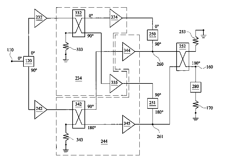
2o Shown in figure 5 is a Doheriy amplifier according to the invention. The
driver amplifiers
(232 and 242) are balanced or single ended as shown in figures 4 and 5. The
main final stage
amplifier (234) comprises first and second main paired amplifiers (334 and
335) that are fed
from a main power splitter (332). The auxiliary final stage amplifier (244)
comprises first and
second auxiliary paired amplifiers (344 and 345) that are fed from an
auxiliary power splitter
(342). The power splitters (332 and 342) comprise two outputs substantially
90° different in
phase and equal in amplitude.
CA 02559780 2006-09-13
WO 2005/088830 PCT/GB2005/000942
-9-
Reflections from both pairs of amplifiers (334 with 335 and 344 with 345)
travel back through
their associated power splitter (332 or 342 respectively). At the common input
of the splitters
the two reflected signal are out of phase by 180° and cancel each other
out. At the terminated
port of each splitter the pair of reflected signals are in phase and add
together. They are then
dissipated in the associated load resistor (333 or 343, respectively).
The outputs from the four amplifiers (334, 344, 335 and 345) are then paired
so that they can
be configured in the same way as in a known Doherty amplifier. That is each
main amplifier
(334 or 335) output is then connected on a corresponding auxiliary amplifier
(344 or 345)
output via a respective impedance inverter (250, 251). The circuitry before
the amplifiers
to must maintain the phase offset required that ensures that the phase of each
auxiliary amplifier
(344 or 345) output must be delayed relative to the main amplifier (334 or
335) output that it
is paired with, in order to compensate for the phase offset of the impedance
inverters (250 and
251) that they later recombine through. Both main amplifiers (334 and 335) now
continue to
see an effective reduction in load impedance as the auxiliary amplifiers (344
and 345) turn on.
The output powers, of both main amplifiers (334 and 335), increase with
increased input
power, while their efficiency is maintained.
The balancing configuration of the final stage amplifiers (234 and 244) is
then completed
using a combiner (252) after the common points (260 and 261), just prior to
the last
impedance transformer (280) and the load (170).
2o The combiner comprises first and second input ports and a output port. The
combiner
introduces a phase difference between the signals received at the input ports
before combining
them at the output port. The phase difference is opposite to that of the phase
difference
introduced by the auxiliary power splitter, ie -90° in this embodiment.
Shown in figure 6 is a further embodiment of a Doherty amplifier according to
the invention.
The principle of operation is similar to that of figure 5 except the driver
amplifiers (232 and
242) comprise balanced pairs of amplifiers. The outputs of the amplifiers are
connected to
90° power splitters as shown to reduce reflections between these
amplifiers.
CA 02559780 2006-09-13
WO 2005/088830 PCT/GB2005/000942
-10-
The output from the main and auxiliary driven amplifiers are connected to the
main and
auxiliary power sputters as previously described.
Two further embodiments are depicted in figures 7 and 8, respectively. In
these embodiments
an impedance transformer 281 is connected in the main signal path immediately
before the
combiner 252, between the common node 260 connecting the main amplifier 334
and
auxiliary amplifier 344 and the combiner 252. A corresponding impedance
transformer 282 is
connected in the auxiliary signal path immediately before the combiner 252,
between the
common node 261 connecting the main amplifier 335 and auxiliary amplifier 345
and the
combiner 252.
to The power splitter of these embodiments is a 3dB coupler.
The transistors of these embodiments are GaAs transistors. In other
embodiments the
transistors can be silicon LDMOS, GaN and SiC. Any transistor technology is
suitable
provided the auxiliary amplifier ( 140) can appear as an approximate open
circuit when it
switches off.
In these embodiments the impedance inverters (150 and 280 are implemented as
microstrip
transmission lines. Inverter (150) is 3852 and inverter (280) is 30.86SZ.
Other formats and
values are possible as the above values are specific to the embodiment
described.
Surface mount stripline couplers are used as splitter/combiner elements.
Again, other formats
are possible.