Note : Les descriptions sont présentées dans la langue officielle dans laquelle elles ont été soumises.
CA 02560688 2006-09-20
WO 2005/104254 PCT/US2005/001934
ETCHING OF SUBSTRATES OF LIGHT EMITTING DEVICES
Field of the Invention
This invention relates to semiconductor light emitting devices and fabricating
methods therefor.
Background of the Invention
Semiconductor light emitting devices, such as Light Emitting Diodes (LEDs)
or laser diodes, are widely used for many applications. As is well known to
those
having skill in the art, a semiconductor light emitting device includes a
semiconductor
light emitting element having one or more semiconductor layers that are
configured to
emit coherent and/or incoherent light upon energization thereof. As is well
known to
those having skill in the art, a light emitting diode or laser diode generally
includes a
diode region on a microelectronic substrate. The microelectronic substrate may
.be,
for example, gallium arsenide, gallium phosphide, alloys thereof, silicon
carbide
and/or sapphire. Continued developments in LEDs have resulted in highly
efficient
and mechanically robust light sources that can cover the visible spectrum and
beyond.
These attributes, coupled with the potentially long service life of solid
state devices,
may enable a variety of new display applications, and may place LEDs in a
position to
compete with the well entrenched incandescent and fluorescent lamps.
Published United States Patent Application No. 2002/0123164, the disclosure
of which is incorporated herein as if set forth in its entirety, describes
light emitting
diodes that include a substrate having first and second opposing faces and
that is
transparent to optical .radiation in a predetermined wavelength range and that
is
patterned to define, in cross-section, a plurality of pedestals that extend
into the
substrate from the first face towards the second face. A diode region on the
second
face is configured to emit light in the predetermined wavelength range, into
the
substrate upon application of voltage across the diode region. A mounting
support on
the diode region, opposite the substrate is configured to support the diode
xegion, such
that the light that is emitted from the diode region into the substrate, is
emitted from
the first face upon application of voltage across the diode region. The first
face of the
CA 02560688 2006-09-20
WO 2005/104254 PCT/US2005/001934
substrate may include therein a plurality of grooves that define a plurality
of
triangular pedestals in the substrate. The grooves may include tapered
sidewalls
and/or a beveled floor. The first face of the substrate also may include
therein an array
of via holes. The via holes may include tapered sidewalls and/or a floor.
In GaP light emitting devices, the devices have been conventionally singulated
using a two-step sawing process. To define a mesa of the GaP device, a first
series of
wide saw blade saw cuts is made in a wafer of GaP device and then the saw cuts
are
etched using a GaP aqueous etchant to remove damage from the saw cut.
Subsequent
saw cuts are then made using a thinner saw blade to singulate the GaP devices.
Techniques for dry etching laser light cut light emitting diodes are described
in
United States Patent No. 5,912,477, the disclosure of which is incorporated
herein by
reference as if set forth fully herein.
Summary of the Invention
Some embodiments of the present invention provide for fabrication of a light
emitting device including a silicon carbide substrate having first and second
opposing
faces and a light emitting element on a first face of the substrate by
directly etching
the second face of the silicon carbide substrate using an aqueous etch to
remove a
damaged portion of the substrate resulting from processing of the substrate.
The
damaged portion of the second face of the silicon carbide substrate may result
from
sawing the substrate, lapping the substrate, polishing the substrate,
implantation in the
substrate and/or laser processing the substrate.
In certain embodiments of the present invention, directly etching the second
face of the silicon carbide substrate is carried out subsequent to singulation
of the
light emitting device from a wafer. In other embodiments of the present
invention,
directly etching the second face of the silicon carbide substrate is carried
out prior to
singulation of the light emitting device from a wafer.
In some embodiments of the present invention, the aqueous etch is an etch
with KOH:K3Fe(CN)6.
In additional embodiments of the present invention, directly etching the
second face of the silicon carbide substrates includes etching a carbon-faced
surface
of the silicon carbide substrate andlor etching a non-carbon-faced surface of
the
silicon carbide substrate. The carbon-faced surface may be a sidewall of the
substrate.
CA 02560688 2006-09-20
WO 2005/104254 PCT/US2005/001934
In certain embodiments of the present invention, directly etching the second
face of the silicon carbide substrate includes directly etching a surface
oblique to the
second face of the silicon carbide substrate.
In further embodiments of the present invention, light output of a light
emitting device is increased by etching a substrate of the light emitting
device using
an aqueous etch to remove a light absorption region of the substrate of the
light
emitting device. The light absorption region may correspond to a region of the
substrate damaged by processing the substrate in fabrication of the light
emitting
device. For example, the region of the substrate damaged by processing the
substrate
may correspond to a saw groove in the substrate. The region of the substrate
damaged
by processing the substrate could also correspond to a lapped, polished and/or
laser
processed region of the substrate.
In certain embodiments of the present invention, the substrate is a silicon
carbide substrate. Furthermore, etching a substrate may include etching a
carbon face
of the silicon carbide substrate and/or etching a non-carbon face of the
silicon carbide
substrate.
In additional embodiments of the present invention, the substrate is a
sapphire
substrate.
In some embodiments of the present invention, etching the substrate is carried
out subsequent to singulation of the light emitting device. The aqueous etch
may
include etching with KOH:K3Fe(CN)6. The aqueous etch may be carried out for at
least about 50 minutes. The aqueous etch may be carried out at a temperature
of at
least about 80 °C. Furthermore, etching a substrate may be provided by
directly
etching the substrate.
In yet other embodiments of the present invention, fabrication of a light
emitting device includes etclung a substrate of the light emitting device
using an
aqueous etch having etching parameters that are sufficient to increase an
amount of
light extracted through the substrate. The etch of the substrate may include
etching
the substrate to remove at least a portion of a region of the substrate
damaged by
processing the substrate in fabrication of the light emitting device. The
region of the
substrate damaged by processing the substrate may correspond to a saw groove
in the
substrate. The region of the substrate damaged by processing the substrate
could also
correspond to a lapped, polished, implanted and/or laser processed region of
the
substrate.
CA 02560688 2006-09-20
WO 2005/104254 PCT/US2005/001934
In particular embodiments of the present invention, the substrate is a silicon
carbide substrate. Etching the substrate may include etching a carbon face of
the
silicon carbide substrate and/or etching a non-carbon face of the silicon
carbide
substrate. The carbon face of the substrate may be a carbon faced sidewall of
the
substrate.
In certain embodiments of the present invention, the substrate is a sapphire
substrate.
In some embodiments of the present invention, etching the substrate sufficient
to increase an amount of light extracted through the substrate is carried out
subsequent to singulation of the light emitting device. The aqueous etch may
include
etching with KOH:K3Fe(CN)6. The aqueous etch may be carried out for at least
about
50 minutes. The aqueous etch may also be carried out at a temperature of at
least
about 80 °C. Etching the substrate sufficient to increase an amount of
light extracted
through the substrate may include directly etching the substrate.
In additional embodiments of the present invention, fabricating a light
emitting device includes etching a silicon carbide substrate of the light
emitting
device using an aqueous etch to remove at least a portion of amorphous silicon
carbide from a surface of the silicon carbide substrate of the light emitting
device.
The amorphous silicon carbide may correspond to a region of the substrate
damaged
by processing the substrate in fabrication of the light emitting device. The
region of
the substrate damaged by processing the substrate may correspond to a saw
groove in
the substrate, a lapped, polished, implanted and/or laser processed region of
the
substrate.
In further embodiments of the present invention, etching a silicon carbide
substrate of the light emitting device to remove at least a portion of
amorphous silicon
carbide from a surface of the silicon carbide substrate is carried out
subsequent to
singulation of the light emitting device.
The aqueous etch may include etching with KOH:K3Fe(CN)6. The aqueous
etch may be carried out for at least about 50 minutes. The aqueous etch may be
carried out at a temperature of at least about 80 °C. Etching a silicon
carbide substrate
of the light emitting device to remove at least a portion of amorphous silicon
carbide
from a surface of the silicon carbide substrate may be provided by directly
etching the
substrate.
CA 02560688 2006-09-20
WO 2005/104254 PCT/US2005/001934
In still further embodiments of the present invention, fabricating a light
emitting device includes sawing a silicon carbide substrate of the light
emitting device
and etching at least one sawn surface of the silicon carbide substrate of the
light
emitting device. Etching at least one sawn surface may include etching a
carbon face
of the silicon carbide substrate and/or etching a non-carbon face of the
silicon carbide
substrate.
In some embodiments of the present invention, etching at least one sawn
surface is carried out subsequent to singulation of the light emitting device.
Etching
at least one sawn surface may also be provided by performing an aqueous etch
of the
substrate. The aqueous etch may include etching with KOH:K3Fe(CN)6. The
aqueous etch may be carried out for at least about 50 minutes. The aqueous
etch may
be carried out at a temperature of at least about 80 °C. Etching at
least one sawn
surface may include directly etching at least one sawn surface.
Brief Description of the Drawings
Figure 1 is a flowchart illustrating fabrication steps according to
embodiments
of the present invention.
Figure 2 is a flowchart illustrating fabrication steps according further
embodiments of the present invention.
Figures 3A and 3B are cross-sectional views of a light emitting device before
and after etching according to further embodiments of the present invention.
Detailed Description
The present invention now will be described more fully hereinafter with
reference to the accompanying drawings, in which embodiments of the invention
are
shown. This invention may, however, be embodied in many different forms and
should not be construed as limited to the embodiments set forth herein.
Rather, these
embodiments are provided so that this disclosure will be thorough and
complete, and
will fully convey the scope of the invention to those skilled in the art. In
the
drawings, the size and relative sizes of layers and regions may be exaggerated
for
clarity. Like numbers refer to like elements throughout. As used herein, the
term
"andlor" includes any and all combinations of one or more of the associated
listed
items.
CA 02560688 2006-09-20
WO 2005/104254 PCT/US2005/001934
It will be understood that, although the terms first, second, etc. may be used
herein to describe various elements, components, regions, layers and/or
sections, these
elements, components, regions, layers and/or sections should not be limited by
these
terms. These terms axe only used to distinguish one element, component,
region,
layer or section from another region, layer or section. Thus, a first element,
component, region, layer or section discussed below could be termed a second
element, component, region, layer or section without departing from the
teachings of
the present invention.
Some embodiments of the present invention provide methods for fabricating
light emitting devices by etching at least one damaged surface of a substrate
of the
device so as to remove at least a portion of the damaged surface. While not
being
bound by any particular theory of operation, it is believed that a light
absorption
region of the light emitting device may result from processing operations
performed
on the light emitting device, such as sawing the device to singulate the
device and/or
to create light extraction features of the device, lapping, polishing,
implantation
and/or laser processing the device. The light absorption region may result
from
damage to the substrate and/or layers of the device as a result of processing
the
substrate and/or layers of the device. Thus, by etching the damaged surface of
the
light emitting device some or all of the light absorption region may be
removed,
thereby increasing the light extracted from the device.
Embodiments of the present invention may be suitable for fabricating
semiconductor light emitting devices, such as a light emitting diode, laser
diode
and/or other semiconductor device which includes one or more semiconductor
layers,
which may include silicon, silicon carbide, gallium nitride andlor other
semiconductor
materials, a substrate which may include sapphire, silicon, silicon carbide
and/or other
microelectronic substrates, and one or moxe contact layers which may include
metal
and/or other conductive layers. In some embodiments, ultraviolet, blue and/or
green
LEDs may be provided.
For example, the light emitting devices may be gallium nitride-based LEDs or
lasers fabricated on a silicon carbide substrate such as those devices
manufactured and
sold by Cree, Inc. of Durham, North Carolina. The present invention may be
suitable
for use with LEDs and/or lasers as described in United States Patent Nos.
6,201,262;
6,187,606; 6,120,600; 5,912,477; 5,739,554; 5,631,190; 5,604,135; 5,523,589;
5,416,342; 5,393,993; 5,338,944; 5,210,051; 5,027,168; 5,027,168; 4,966,862
and/or
CA 02560688 2006-09-20
WO 2005/104254 PCT/US2005/001934
4,918,497, the disclosures of which are incorporated herein by reference as if
set forth
fully herein. Other suitable LEDs and/or lasers are described in published
U.S. Patent
Publication No. US 2003/0006418 A1 entitled Group III Nitride Based Light
Emitting
Diode Sty~uetures With a Quantum Well and Supe~lattice, Group III Nitride
Based
Quantum Well Structures and Group III Nitride Based Super~lattice Structures,
published Januaxy 9, 2003, as well as published U.S. Patent Publication No. US
2002/0123164 A1 entitled Light Emitting Diodes Including Modifications for
Liglzt
Extraction and Manufacturing Methods Therefor. Furthermore, phosphor, coated
LEDs, such as those described in U.S. Application Serial No. 10/659,241,
entitled
Phosphor-Coated Light Emitting Diodes Including Tapered Sidewalk and
Fabrication Methods Therefor, filed September 9; 2003, the disclosure of which
is
incorporated by reference herein as if set forth fully, may also be suitable
for use in
embodiments of the present invention. The LEDs and/or lasers may be configured
to
operate such that light emission occurs through the substrate. Tn such
embodiments,
the substrate may be patterned so as to enhance light output of the devices as
is
described, for example, in the above-cited U.S. Patent Publication No. US
2002/0123164 Al.
Methods of fabricating light emitting devices according to some embodiments
of the present invention are illustrated in Figure 1. As seen in Figure 1, a
substrate
of a light emitting device is processed in the fabrication of the light
emitting device
(block 100). This processing results creating a light absorption region in the
substrate
such that, in operation, at least some light is absorbed in the substrate by
the light
absorption region. As discussed above, this light absorption region may result
from
damage to the substrate resulting from the processing of the substrate. For
example,
the processing of the substrate may result in an amorphous region of the
substrate
being formed.
The processed substrate is then etched in an aqueous etch (block 110). The
etch may remove some or all of the light absorption region and/or damaged
region
resulting from the processing of the substrate. For example, if the processing
of the
substrate results in an amorphous region, some or alI of the amorphous region
may be
removed. By etching substrates of light emitting devices after processing the
substrates, the light output of the light emitting device may be increased.
For
example, as discussed below, for silicon carbide substrates with gallium
nitride based
light emitting elements, the light output of the light emitting device has
been found to
CA 02560688 2006-09-20
WO 2005/104254 PCT/US2005/001934
increase as a result of aqueous etching the device after the device has been
sawn to
provide light extraction features in the substrate of the light emitting
device.
In particular embodiments of the present invention, the substrate is a silicon
carbide substrate. In other embodiments of the present invention, the
substrate is a
sapphire substrate. The processing of the silicon carbide substrate may
include
sawing the silicon carbide substrate, for example, to provide light extraction
features
in the silicon carbide substrate and/or to singulate the light emitting device
from a
wafer that includes multiple light emitting devices. The processing of the
silicon
carbide substrate could also include laser processing of the light emitting
substrate,
for example to provide laser ablation, feature patterning and/or singulation
of the light
emitting device. The processing of the silicon carbide substrate could also
include
lapping and/or polishing of the substrate. Processing the silicon carbide
substrate
could also include implantation in the silicon carbide substrate. The
processing of the
silicon carbide substrate may occur before, during or after formation of a
light
emitting element on the substrate.
The etching of the substrate may be provided by any suitable etching
technique capable of etching the substrate. In particular embodiments of the
present
invention where the substrate is silicon carbide, the etch may be any etch
capable of
etching silicon carbide. An aqueous etch may be carried out in a mufti-wafer
manner
before or after singulation and, therefore, may be more amenable to scaling to
commercial production. Accordingly, in some embodiments of the present
invention,
the etch is an aqueous etch. For example, the etch may be an etch with
KOH:K3Fe(CN)6. A suitable etchant is provided by Transene Corporation of
Rowley,
Massachusetts, as a GaP etchant. Suitable etchants for sapphire may include,
for
example, H3PO4 and/or a mixture of H3P04:H2S04.
In some embodiments, the silicon carbide is directly etched. As used herein,
directly etched refers to etching the silicon carbide to remove silicon
carbide without
first converting the silicon carbide to another material, such as an oxide. In
some
embodiments, the light absorbing region may first be converted to an oxide and
then
the oxide removed. Techniques using a sacrificial oxide to remove damaged
silicon
caxbide axe well known and, therefore, will not be described further herein.
See e.g.,
Chapter 4, "Process Technology for Silicon Carbide Devices" by Carl-Mikael
Zetterling (2002); see also, United States Patent No. 6,214,107, the
disclosure of
which is incorporated herein by reference as if set forth in its entirety. Use
of a
CA 02560688 2006-09-20
WO 2005/104254 PCT/US2005/001934
sacrificial oxide for damage removal may be difficult in practice, however,
where the
devices are etched after singulation because of the high temperatures
typically utilized
to oxidize silicon carbide may melt the blue tape or other carrier to which
the devices
are attached.
The particular conditions under which the etch is carried out may depend on
the etching agent utilized, the nature of the processing that caused the
damage, the
characteristics of the light absorption/damaged region and/or the amount of
substrate
material to be removed. Such condition may, for example, be selected for a
particular
processing operation by, for example, experimentally determining light output
of
similarly processes devices using differing etching conditions (e.g. time
and/or
temperature) and selecting etching conditions based on the light output.
However, in
particular embodiments of the present invention where the substrate is silicon
carbide,
the damage results from sawing the substrate and the etch is carried out with
I~OH:I~3Fe(CN)6, the etch may be carried out at a temperature of at least
about 80 °C,
for example, from about 80 to 90 °C for at least about 50 minutes, for
example, from
about 50 minutes to about one hour. Other times and/or temperatures may also
be
used. Accordingly, embodiments of the present invention should not be
construed as
limited to the particular exemplary etching parameters described herein.
In some embodiments of the present invention, the etching etches a carbon
face of the silicon carbide substrate and/or a non-carbon face of the silicon
carbide
substrate. The etching may also etch a surface of the substrate that is
oblique to a
surface of the substrate opposite the surface of the substrate on which the
light
emitting element is formed. As used herein, oblique refers to a surface that
is non-
parallel to a reference surface.
Figure 2 is a flowchart illustrating fabrication steps according to some
embodiments of the present invention. As seen in Figure 2, a substrate of a
light
emitting device is sawn to provide light extraction features and/or to
singulate devices
on a wafer (block 200). This processing results creation of a light absorption
region
in the substrate such that, in operation, at least some light is absorbed in
the substrate
by the light absorption region in the substrate. As discussed above, this
light
absorption region may result from damage to the substrate resulting from the
sawing
of the substrate. For example, the sawing of the substrate may result in an
amorphous
region of the substrate being formed.
CA 02560688 2006-09-20
WO 2005/104254 PCT/US2005/001934
At least one sawn surface of the substrate is then etched (block 210). The
etch
may be carried out so as to xemove some or all of the light absorption region
and/or
damaged region resulting from the processing of the substrate. For example, if
the
sawing of the substrate results in an amorphous region, some or all of the
amorphous
region may be removed. By etching substrates of light emitting devices after
the
substrates are sawn, the light output of the light emitting device may be
increased.
In some embodiments of the present invention, the etch of the sawn surface is
a day etch and/or an aqueous etch. In particular embodiments of the present
invention, the etch is an Inductively Coupled Plasma (ICP) etch. However, an
ICP
etch is typically carried out on a wafer-by-wafer basis and, therefore, may
pxesent
difficulties in scaling to commercial production. An aqueous etch may be
carried out
in a mufti-wafer manner before or after singulation and, therefore, may be
more
amenable to scaling to commercial production. Accordingly, in some embodiments
of the present invention, the etch is an aqueous etch. For example, the etch
may be an
etch with KOH:K3Fe(CN)6. A suitable etchant is provided by Transene
Corporation
of Rowley, Massachusetts, as a GaP etchant. Suitable etchants for sapphire
rnay
include, for example, H3PO4 and/or a mixture of H3P04:H2S04.
The etch of the sawn substrate may occur before or after singulation of the
devices. In some embodiments of the present invention, a blue tape or other
carrier is
applied to the wafer, the wafer is then sawn to singulate the devices and then
etched
while the singulated devices remain on the blue tape. The devices may also be
sawn
to provide light extraction features as described, for example, in published
United
States Patent Application No. US 2002/0123164 Al.
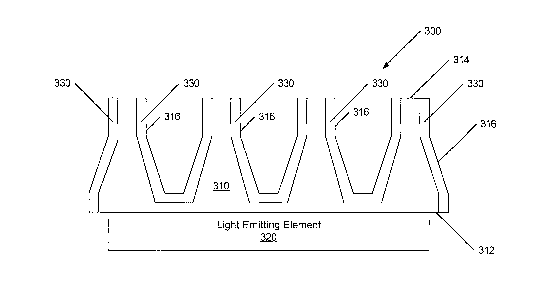
Figure 3A is a cross-section of a Iight emitting device 300 prior to etching
according to some embodiments of the present invention. As seen in Figure 3A,
a
light emitting element 320 is foamed on a first surface 312 of a substrate
310. As
discussed above, the substrate 310 may be a silicon carbide substrate and, in
particular, a single crystal silicon carbide substrate. In some embodiments of
the
present invention, the substrate 310 is a sapphire substrate. The substrate
310 has
formed in it a plurality of light extraction features as illustrated by the
trenches in a
second surface 314 of the substrate 310. The second surface 314 of the
substrate is
opposite the first surface 312 of the substrate 310. As discussed above, the
trenches
may be formed, for example, by sawing the substrate 310. The trenches have
sidewalk that include a surface 316 that is oblique to the second surface 314
of the
to
CA 02560688 2006-09-20
WO 2005/104254 PCT/US2005/001934
substrate 310. As used herein, a sidewall of the substrate includes the outer
edges of
the substrate and/or sidewall of a trench or feature that terminates within
the substrate
or extends through the substrate. In particular embodiments of the present
invention,
the second surface 314 of the substrate 310 is a carbon face of a silicon
carbide
substrate. In such embodiments, the oblique surfaces 316 (sidewalls) may
include
non-carbon faces of the silicon carbide substrate (e. g. the perpendicular
portion of the
oblique surfaces 316) as well as carbon faces of the silicon carbide substrate
(e.g. the
beveled portion of the oblique surfaces 316).
As a result of the processing of the substrate 310, light absorption regions
330
may be formed in the substrate 310. The light absorption regions 330 may
correspond
to damaged regions of the substrate 310. In some embodiments of the present
invention, the light absorption regions 330 are regions of amorphous silicon
carbide.
While the light absorption regions 330 are illustrated on the oblique surfaces
316,
light absorption regions may also exist on other surfaces, such as on the
second face
314 of the substrate 310. Furthermore, while the light absorption regions 330
are
illustrated in Figure 3A as continuous regions of substantially uniform
thickness, the
regions may be discontinuous and/or of non-uniform thickness.
The light emitting device 300 of Figure 3A is etched as described above to
remove at least a portion of the light absorption regions 330 to provide the
light
emitting device 300' as illustrated in Figure 3B. The etch of the substrate
310 etches
the oblique surfaces 316 to remove at least a portion of the light absorption
regions
330. Thus, the etch may etch a non-carbon face of a silicon carbide substrate
and a
carbon face of the silicon carbide substrate. The etch may also etch the
second
surface 314 and surfaces parallel to the second surface 3I4 (such as the
bottoms of the
trenches) and, therefore, the etch may etch a carbon face of the silicon
carbide
substrate as well.
The light emitting device 300 is etched using etching parameters that are
sufficient to increase the amount of light extracted from the substrate of the
light
emitting device 300' to be greater than the amount of light extracted from the
substrate 310 of the light emitting device 300. In some embodiments, the etch
is
performed to remove all of the light absorption regions 330 from the substrate
310.
However, because the light absorption regions 330 may be non-uniform in
thickness
andlor because the location of the light absorption regions 330 may affect the
light
output of the light emitting device differently, some of the light absorption
regions
11
CA 02560688 2006-09-20
WO 2005/104254 PCT/US2005/001934
330 may remain in the substrate 310 after etching. For example, if a one hour
etch
achieves 99.9 percent of the light output as a four hour etch, from a
manufacturing
standpoint, it may be advantageous to utilize the one hour etch rather than
the four
hour etch even though some of the light absorption regions 330 may remain in
the
substrate 310. In other embodiments of the present invention, over-etching may
be
performed to ensure that all of the light absorption regions 330 are removed.
The following examples are provided for illustrative purposes and are not
intended to limit the scope of the present invention.
Examples
The light output of XB900, XB300 and XB500 light emitting diodes from
Cree Inc., Durham, North Carolina, was measured before and after etching
according
to embodiments of the present invention. The XB900, XB300 and XB500 diodes axe
gallium nitride based diodes on a silicon carbide substrate. The diodes are
sawn for
singulation and to create light extraction features at least at the periphery
of the
devices.
In a first test, XB900 light emitting diodes were etched for approximately one
hour in KOH:K3Fe(CN)6 at a temperature of from about 80 to 90 °C. The
light
emitting diodes were encapsulated in Dymax (UV) doming on TO-18 headers. Table
1 reflects the output of the devices with a 20mA drive current.
Table 1. XB900 Light Output
Part # Initial After Etch(after/initial)Dymax er (dymax/initial)
1 8.52 9.98 1.17 17.2 2.02
2 8.91 10.6 1.19
3 9.29 10.8 1.16
4 8.93 10.3 1.15 17.6 1.97
8.77 10.1 1.15
6 9.13 NO 16.2 1.77
7 9.22 NO 16.4 1.7 8
8 8.95 NO
In Table 1, the Initial column is the light output of the device prior to
etching as
measured in milliwatts (mW). The After Etch column is the light output of the
device
after etching as measured in mW. A NO in the After Etch column indicates a
control
12
CA 02560688 2006-09-20
WO 2005/104254 PCT/US2005/001934
group where no etching was performed. The (after/initial) column is the
percent gain
of a bare chip. The Dymax er column is mWs of radiant flux of Dymax
encapsulated
LED dice. The (dymaxlinitial) column is the percent gain of unetched dice/chip
to
encapsulated parts (indicating higher light extraction fox etched parts.
XB300 light emitting diodes, XB500 light emitting diodes and XB900 light
emitting diodes were also tested. The light output of the diodes was measured
before
and after etching in KOH:K3Fe(CN)6 for approximately 50 minutes. The diodes
were
mounted on a TO-18 header with no encapsulation. The results of the test are
reflected in Table 2.
Table 2. XB300, XB500 and XB900 Light Output
XB300 XB500 XB900
Initial After Initial After EtchInitial After Etch
Etch
9.6 11.1 6.29 7.01 9.02 10.4
9.86 11.4 6.49 7.42 8.86 10.1
10.7 12 6.67 7.46 8.8 10.1
It will be understood by those having skill in the art that various
embodiments
of the invention have been described individually in connection with Figures 1-
3B.
However, combinations and subcombinations of the embodiments of Figures 1-3B
may be provided according to various embodiments of the present invention.
As seen from Table 1, light output of the XB900 LEDs of Table 1 increased
by approximately 13-15% after etching. As seen from Table 2, light output of
the
XB300 and XB900 increased approximately 15-16% and light output from the XB500
increased approximately 11-12% after etching. Thus, based on the results
above, it
appears that etching of the substrates of the light emitting diodes is
effective in
increasing the amount of light extracted through the substrate of the diodes.
In the drawings and specification, there have been disclosed embodiments of
the invention and, although specific terms are employed, they are used in a
generic
and descriptive sense only and not for purposes of limitation, the scope of
the
invention being set forth in the following claims.
13