Note : Les descriptions sont présentées dans la langue officielle dans laquelle elles ont été soumises.
CA 02561570 2006-09-28
WO 2004/085969 PCT/CA2004/000475
-1-
REMOTELY PROGRAMMABLE INTEGRATED SENSOR TRANSMITTER
FIELD OF THE I~llfEi~TION
This invention relates to temperature sensors, more particularly to a
temperature sensor including an RTD element, a conditioning circuit, a scalar
unit
and a combined digital and analog transmitter, all in a single compact
assembly.
The remotely programmable integrated sensor transmitter can also be re-
calibrated and re-scaled over its entire range (-200° O to 300°
C).
BAOI~GR~UI~D OF THE I~~~EI~TIOI~
The temperature is often a critical variable that needs to be measured
accurately in various industrial processes. Today, the RTD (Resistive
Temperature Detector) is the most popular device used in temperature control.
With an RTD element, we can obtain a resolution of hundredth or even
thousandths of a degree centigrade in an ambient or moderate temperature
application.
The temperature cannot be measured directly from the RTD element. It has
to be calculated from the measurement of a dependant variable that has a known
relation with the temperature at which it is exposed. Unfortunately this
relation,
which is well known by the people working in this field, is not linear and for
most of
the application it is not convenient to have a non-linear signal. To solve
this
problem, many solutions have been proposed. German Patent No. 2,459,623 to
Bruyere discloses a design in which an extra resistor is connected between an
amplifier output and input and a referenced resistor. This method of
linearization is
not that accurate, greater than one part in thousand over the entire range,
and is
also highly dependent on the component tolerance used in the circuit. That,
obviously, poses manufacturing problems.
Other techniques have been proposed in U.S. Pat. No. 4,000,454 and U.S.
Pat. No. 4,556,330 where they used an external linearization apparatus in
which
the voltage impressed to the conditioning section (a Ullheatstone Bridge)
changes
as the resistance ~f the element changes. However, this arrangement contained
also some disadvantages. First, the external placement of the lineari~ation
module
provides, often, inaccurafie readings by the fact that the sensing element and
the
CA 02561570 2006-09-28
WO 2004/085969 PCT/CA2004/000475
-2
linearization module are not integrated. Secondly, those devices are known to
be
unstable, whereby the failure of one or more components result in the failure
of
the entire device. Finally, the use of separate components increases the
manufacturing and installation cost and can also be a problem on installation
where the clearance is limited.
To overcome those problems, the IJ.S. Pat. 5,741,074 proposed a linear
integrated sensing transmitter. This transmitter integrates, in a single
housing, the
temperature sensing device and a current transmitter. The lineari~ation is
performed via a feedback resistor, a return path resistor, and a constant
current
source, all connected to a voltage-to-current converter. This arrangement
gives a
good linearization and offers an accuracy of <0.1 % of the full-scale.
However, this
device has also many lacks. First, the device cannot be calibrated to take in
account the tolerance of the RTD element or the components themselves. That
implies problems in a manufacturing point of view by the fact that we have to
take
a special care to the components selection. If the device is not perfectly
linear, or
offset, there is no way to correct it. Secondly, to change the range of
operation of
the device, we have to re-calculate and change all the resistor values. That
is also
causing a problem because we need different configurations for different
ranges
of operation.
The purpose of the present invention is to overcome those problems by
suggesting an integrated transmitter, which includes the sensing element, a
current transmitter and a scalar unit. The scalar unit gives more flexibility
to the
device and allows the calibration and re-scaling of the device via a digital
communication between the device itself, and a hand-held programmer or a
computer. '
SUMMARY OF THE INVENTION
Accordingly, an object of the present invention is to provide a remotely
programmable sensor and device for measuring a physical quantity of a medium
comprising, a sensor for measuring the physical quantity ~f the medium and
providing an electrical output within an operational range; a sealer module
for
receiving the electrical output and for producing a scaled analog signal as a
function of the electrical output and a scale selection definition and a data
CA 02561570 2006-09-28
WO 2004/085969 PCT/CA2004/000475
-3-
interface for receiving programming data from an external computer and for
providing the scale selection definition to the scalar module, such that the
operational range of the electrical output is matched to cover a device output
range so as to provide maximum sensitivity to the device.
According to another object of the present invention, there is provided a
method for measuring a physical quantity of a medium, comprising, generating
an
electrical measurement value representative of the physical quantity of the
medium from a sensor, the physical quantity lying within an operational range;
receiving programming data from an external computer including a scale
selection
definition, allowing to scale a signal within the operational range to be
within a
desired output range; and producing a scaled analog signal output within the
desired output range from the electrical measurement value and the scale
selection definition.
According to yet another object of the present invention, there is provided a
remotely programmable device for measuring a physical quantity of a medium to
be attached to a separate sensor unit.
BRIEF DESCRIPTION OF THE DRAWINGS
The other features and advantages of the invention will be apparent from
the following detailed description of each drawing.
Fig.1 represents the mechanical construction of the integrated sensor
transmitter.
Fig. 2 is a block diagram of the integrated sensor transmitter circuit.
Fig. 3 is a block diagram of a digital embodiment of the present invention.
Fig. 4 is a block diagram of an analog embodiment of the present invention.
Fig. 5a is a block diagram of the remotely programmable integrated sensor
transmitter configured for RS-232 communication.
Fig. 5b is a block diagram of the remotely programmable integrated sensor
transmitter configured for RS-485 communication.
Fig. 5c is a block diagram of the remotely programmable integrated sensor
transmitter configured for FShC communication with HART protocol.
Fig. 6 represents the flow chart of the program inside the scalar unit
Fig. 7 is a tree diagram of the different calibration procedures available to
CA 02561570 2006-09-28
WO 2004/085969 PCT/CA2004/000475
-4-
the remotely programmable integrated sensor.
DETe411_E~ ~E~CI~IPTI~f~ OF THE PF~EFEI~I~E~ E~IIB~~II~IEP~T
A~llith reference now to Fig.1 there is shown an exemplary embodiment of
the integrated resistance temperature detector and transmitter of the present
invention. The device comprises an elongated cylindrical housing 11,13 for
receiving a miniaturised transmitter 15 coupled to a resistance temperature
detector 17, 19.
The housing 11,13 is preferably fabricated from InconelT~ or a 316
stainless steel, although it can be fabricated from any suitable metal which
is
capable of protecting the sensing element 17,19 while quickly responding to
changes in temperature. The housing 11,13 comprises a cylindrical tip portion
13
and a cylindrical transition portion 11. The tip portion 13 and the transition
portion
11 are connected together by crimping, soldering, bonding or welding the
transition portion around the tip portion 21, the assembled housing 11,13
defines
a cavity therethrough 23,25.
In the exemplary embodiment shown in Fig. 1 the transition portion of the
housing 11 has a length of 2 %" and an outer diameter of 5/8" (0.625). The tip
portion of the housing 13 has a length of 12"and an outer diameter of ~~4". It
should
be understood that the above dimensions are merely illustrative and may be
altered to adapt the sensor to different applications.
Disposed within the cavity of the tip porti~n 25 of the housing is fihe
resistance temperature detector 17, 19 which comprises a 100 ohm, 0.00385
alpha Class B type bulb 17, although a Class A bulb can be substituted.
Disposed
within the bulb is a platinum resistive element 19. The resistive element
17,19
includes a first platinum lead 27 and second platinum lead 29 which extend
from
within the bulb. Again it is to be understood that the present invention is
not
restricted to the above resistance temperature detector; other temperature
sensing means, such as a thermistor or a thermocouple, fall within the scope
of
this invention.
Disposed within the transition portion of the housing 11 is the miniaturised
transmitter 15. The exemplary embodiment shown in Fig. 1 incorporates a
transmitter 15 with 4-20mA output signal 31,33. Again it is to be understood
that
CA 02561570 2006-09-28
WO 2004/085969 PCT/CA2004/000475
-5-
the present invention is not restricted to the above output signal; other
signal
output means, such as voltage, frequency or digital, fall within the scope of
this
invention. The transmitter 15 is miniaturised using well known surface mount
technology. ~4i the input section 39 of the transmitter, there are four
terminals,
comprising of the first, second, third and a fourth input terminals. iViinimum
two
input terminals are required from the sensing element 17,19. At fibs output
section
~.1 of fibs transmitter, there are four terminals comprising a first output
terminal 31
and a second output terminal 33, a first communication terminal 35 and a
second
communication terminal 37. (Additional terminals may be used, depending on the
communication protocol.) The transmitter 15 is secured within the cavity 23 of
the
transition portion of the housing 11 with an amount of sealant or any suitable
potting compound.
The transmitter 15 and the sensor 17, 19 could be manufactured and
assembled together or may be provided as individual components that can be
inter-connected for use.
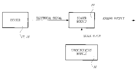
Fig. 2 is a block diagram of a remotely programmable integrated sensor
transmitter. A sensor 17,19 is in primary contact with a process medium,
measuring particular processes of that medium, such as temperature, pressure,
etc. by relating those properties to electrical signals, such as voltage,
current, etc.
In the preferred embodiment, the sensor 17,19 is used for measuring
temperature
and it is a resistance temperature detector, while it could also be a
thermistor, a
thermocouple, an IC sensor, etc. The sensor 17,19 creates an electrical signal
as
a result of a changing property of the process medium. The electrical signal
from
fibs sensor 17, 19 will be in an operational range according to the type of
medium
and the type of application. This operational range is usually different from
the
device output range and a conversion is therefore necessary.
The electrical signal is sent to a sealer module 10. The sealer module 10
receives scale selection definition from a communication module 12. The scale
selection definition could include the parameters necessary for scaling the
electrical signal or it could be a selection of a scale definition from a
plurality of
seals definitions stored in a memory. The scale selection definition allows
the
sealer module 10 to convert the electrical signal received from the sensor 17
into
a scaled analog signal so as to be within a desired output range. The scaled
CA 02561570 2006-09-28
WO 2004/085969 PCT/CA2004/000475
-6-
analog signal produced is then output. The analog signal may be displayed on
an
analog gauge to be connected to the device.
Fig.3 is a block diagram represenfiing one possible embodiment of fihe
infiegrafied sensor firansmififier. Afi fihe exfiremity, fihe Resisfiive
Temperafiure
Defiecfior (RTD) 17 is connected to the condifiioning circuit of the
integrafied sensor
transmififier 16, 18. This conditioning module is composed of a 1/Vheatstone
bridge
16 and an amplifier 18. The bridge 16 produces a small voltage across its
exfiremities when the RTD resisfiance 17 changes with fiemperafiure. This
small
voltage is fihen amplified 18 and directed to the Analog to Digital converter
20. The
condifiioning module 16,18 was designed in such a way as to be able to measure
a change of resistance of the RTD 17 from 15 to 380 ohms. That covers the
entire
range of the integrated sensor transmitter which is -200° to
800°C.
The Analog to Digital converter 20 converts fihe analog signal to a digital
value which is read by a digital sealer 22. The high resolution of the Analog
to
Digital converter 20 allows a high precision measurement over the entire range
of
operation and. eliminates the need for re-scaling the conditioning module. The
Analog to Digital converter 20 has also, a built in auto-calibration feature.
This
feature allows a periodically auto re-calibration of the device to eliminate
any drift
due to a change of temperature.
The Analog to Digital converter and the Digital to Analog converter are
controlled by the digital sealer 10a. The digital sealer 10a receives
calibration
parameters, range information and device information and identification
(address)
from a communication module 12. The communication module 12 is connected to
the external world for exchanging data and calibration of the device via a
digital
communication link 35,37.
The communication module 12 also allows for the device to send the digital
signal to an external computer, where ifi can be analyzed and archived.
The flexibility of the device allows for different modes of communication, as
shown in Fig 5a, 5b and 5c. The sfiandard communication infierFace is RS-232,
buff
a communicafiion interface board can be mounted in piggy back wifih the
infiegrafied sensor firansmitfier fio offer an RS-4.85 or FSI< (Freguency
Shift I~ey)
with HART protocol. The digital communication will be explained in details
later.
Fig. 4 is a block diagram of another.embodiment of the present invention. A
CA 02561570 2006-09-28
WO 2004/085969 PCT/CA2004/000475
-7-
sensor 17,19 is in communication with a conditioning module comprising a
Wheatstone bridge 16 and an amplifier 18 of variable gain. The Bridge 16
produces a small voltage across its extremities when the RTD resistance 16
changes with temperature. This small voltage is then amplified by an amplifier
18
and output as a current signal of 4mA to 20 mA. The conditioning module was
designed in a such way as to be able to measure a cllange of resistance of the
RTD from 15 to 380 ohms, covering the entire range of the integrated sensor
transmitter. A variable resistor 34., such as a potentiometer, is connected in
parallel to the Wheatstone bridge 16 for controlling the resistances therein.
The
variable resistor 34 is controlled by the communication module 12. The
communication module 12 also controls the gain of the ari~plifier 18 in order
to
produce an appropriate analog output value.
DIGITAL COMMUNICATION
The digital communication allows configuration of the integrated sensor
transmitter as well as the identification (address), calibration, re-scaling
and
reading of temperature. Fig. 5a shows the standard serial method of
communication, over two wires with the RS-232 standard . In this
configuration,
the integrated sensor transmitter is connected to an interface communication
module 39a. This module 39a converts the low voltage signal (TTL-5V) 37 to an
RS-232 standard 41 a that can be read by a computer 43 or a hand held
calibrator
49. The module 39a can also provide the power for the integrated sensor
transmitter.
Fig. 5b represents the second method of digital communication available,
the RS-485 standard. The integrated sensor transmitter is connected to an
interface communication module 39b. This module 39b converts the low voltage
signal (TTL-5V) 37 to an RS-485 standard 41 b that can be read by a computer
43
or a hand held calibrator 49. The module 39b can also provide the power for
the
integrated sensor transmitter. The RS-485 standard allows longer distance
between the integrated sensor transmitter itself and the computer 43 or other
calibration device. It also allows for operation of multiple integrated sensor
transmitters connected on the same link, each integrated sensor transmitter
being
identified by its unique address.
CA 02561570 2006-09-28
WO 2004/085969 PCT/CA2004/000475
_$_
Fig. 5c represents the third method of digital communication, via a
Frequency Shift Key (FSK) superimposed on, the current loop. In this
configuration, the interface communication module 39c is a
modulatorldemodulator (fi~lODEi~'l) that converts the signal 37 from the
integrated
sensor transmitter to a FSK and superimposed this frequency signal on the
current loop 41 c. This module 39c is mounted in piggyback with the integrated
sensor transmitter and both are encapsulated in the hand of the integrated
sensor
transmitter. The digital data can then be achieved to a calibrator 49 having
the
FSK implemented or to a computer 43 via a modulator/demodulator (MODEM) 45
which convert the FSK to an RS-232 standard signal 51. The main advantage of
this method of communication is having only two wires coming out of the
integrated sensor transmitter for powering, analog output and digital
communication. In this configuration, the transmitter uses the HART protocol,
which is a well known standard in the industry, to dialogue with other
equipment.
Independently the digital communication used, the 4 to 20 mA current loop
31, 33 is always available to read the temperature. The integrated sensor
transmitter can work as a stand-alone unit without digital communication. The
purpose of the digital communication is to allow for re-calibration or re-
scaling of~
the device.
PROGRAM
In the digital sealer 22, a program manages the functioning of the
integrated sensor transmitter. Fig 6 shows the flow chart of this program.
During
the boot up sequence, the processor first initializes the memory and all the
peripherals 53. After that, it retrieves the calibration and range information
from
the memory 55 and performs the initialization and calibration of the Analog to
Digital converter 57. The program then enters in the main loop and check for
an
external command on the serial port 59. If data is present on serial port,
then the
scalar unit accomplishes the task associated to the code in accordance with
the
communication protocol 51. The next step is to check for auto-calibration of
the
Analog to Digital converter 63. If this is the case the sealer unit commands
the
auto-calibration 65. The following action is the reading of the input signal
from the
sensing element via the Analog to Digital converter 67. The result, under a
digital
CA 02561570 2006-09-28
WO 2004/085969 PCT/CA2004/000475
_g_
format, is then filtered digitally by an algorithm implemented in the
processor 69. If
the result is higher or lower than a certain threshold value, the sensing
element is
considered failed 71. If this is the case the current output is set to a
maximum 87
or minimum 85 value depending the configuration 73. If the signal read from
the
sensing element is in the limit of operation, then a factory offset factor is
applied
75 to it. The factory offset and others calibration features are explain in
the next
section. After the factory offset, the reading is lineari~ed by the processor
77 and
the input 79 and output 81 calibration are performed. Finally, the current
loop is
set 83 to the corresponding reading.
CALIBRATION AND SCALING OF THE REMOTELY PROGRAMMABLE
INTEGRATED SENSOR TRANSMITTER
One of the most important features of this invention is fihe fact that the
device can be re-calibrated and re-scaled at any time without having to change
the device physically. This is a big advantage for a manufacturing point of
view
because all the devices are assembled with the same components. No need to
change any resistors or amplifiers to match a .different range. The fact that
the
device can be calibrated allows also a certain tolerance for all the
components,
including the sensing element. That tolerance is compensated by the
calibration.
For the end-user this is also an advantage. The sensor can be re-scaled for
any
particular application and this mean that the same sensor can work for
different
section of the same process, .which are not in the same temperature range, and
keep a high resolution on the output. The calibration and/or re-scaling are
performed via the digital communication link. Fig. 7 shows all the different
calibrations that can be performed on the integrated sensor transmitter.
A total of 5 different calibrations are available 89. The first one is the
output
calibration 91.This action allows the calibration of the output current
generated by
the Digital to Analog converter. It is performed on two points located at the
extremity of current range, at 4mA 101 and 20 mA 103. Two output calibration
parameters are then calculated by the computer 43 or hand held calibrator 4.9
and
then stored for output calculation.
The second calibration procedure is factory offset 93. The factory offset is
performed by recording the reading form the sensing element at a pre-
determined
CA 02561570 2006-09-28
WO 2004/085969 PCT/CA2004/000475
-10-
temperature 105. This reading represents the offset from this particular
device to
the theoretical values used for linearization.
The third calibration procedure is the operating range 95. The operating
range can be set anywhere inside the total span of the integrated sans~r
transmitter, which is -200° to 300°C. When the range is changed,
default values
of calibration (Zero and Span) are set 10~ to have the output current swings
from
4 to 20 mA between the low and high values of the range. The range value is
stored in the digital scalar module 22.
The fourth calibration procedure is the 1 Point Calibration 97. This
calibration is perform by adjusting the offset parameter 109 in order t~ have
the
output current from the integrated sensor transmitter matched with the known
temperature at which the sensing element is exposed. For this calibration, one
external reference is needed.
Finally, the fifth calibration procedure is the 2 Points Calibration 99. This
calibration is performed when we want to get the most accurate precision form
the
integrated sensor transmitter on a given range. Two external reference points
are
needed for this procedure. When the sensing element is at the first reference
point
the value is then recorded 111 in memory. After, the sensing element is
brought to
the second reference point and the value is recorded 113 in memory. The last
operation is the calculation of the new calibration parameters (Zero and Span)
115. This is performed by the processor in the digital scalar 22 and can be
done at
any time.
It will be understood that numerous modifications thereto will appear to
those skilled in the art. Accordingly, the above description and accompanying
drawings should be taken as illustrative of the invention and not in a
limiting
sense. It will further be understood that it is intended to cover any
variations, uses,
or adaptations of the invention following, in general, the principles of the
invention
and including such departures from the present disclosure as come within known
or customary practice within the art to which the invention perfiains and as
may be
applied to the essential features herein before set forth, and as follows in
the
scope of the appended claims.