Note : Les descriptions sont présentées dans la langue officielle dans laquelle elles ont été soumises.
CA 02564111 2010-12-15
FLUID EJECTION DEVICE
Background
An inkjet printing system, as one embodiment of a fluid ejection system,
may include a printhead, an ink supply that provides liquid ink to the
printhead,
and an electronic controller that controls the printhead. The printhead, as
one
embodiment of a fluid ejection device, ejects ink drops through a plurality of
orifices or nozzles. The ink is projected toward a print medium, such as a
sheet
of paper, to print an image onto the print medium. The nozzles are typically
arranged in one or more arrays, such that properly sequenced ejection of ink
from the nozzles causes characters or other images to be printed on the print
medium as the printhead and the print medium are moved relative to each
other.
CA 02564111 2006-10-18
WO 2005/105455 PCT/US2005/011723
2
In a typical thermal inkjet printing system, the printhead ejects ink drops
through nozzles by rapidly heating small volumes of ink located in
vaporization
chambers. The ink is heated with small electric heaters, such as thin film
resistors referred to herein as firing resistors. Heating the ink causes the
ink to
vaporize and be ejected through the nozzles.
To eject one drop of ink, the electronic controller that controls the
printhead activates an electrical current from a power supply external to the
printhead. The electrical current is passed through a selected firing resistor
to
heat the ink in a corresponding selected vaporization chamber and eject the
ink
through a corresponding nozzle. Known drop generators include a firing
resistor, a corresponding vaporization chamber, and a corresponding nozzle.
As inkjet printheads have evolved, the number of drop generators in a
printhead has increased to improve printing speed and/or quality. The increase
in the number of drop generators per printhead has resulted in a corresponding
increase in the number of input pads required on a printhead die to energize
the
increased number of firing resistors. In one type of printhead, each firing
resistor is coupled to a corresponding input pad to provide power to energize
the firing resistor. One input pad per firing resistor becomes impractical as
the
number of firing resistors increases.
The number of drop generators per input pad is significantly increased in
another type of printhead having primitives. A single power lead provides
power
to all firing resistors in one primitive. Each firing resistor is coupled in
series
with the power lead and the drain-source path of a corresponding field effect
transistor (FET). The gate of each FET in a primitive is coupled to a
separately
energizable address lead that is shared by multiple primitives.
Manufacturers continue reducing the number of input pads and
increasing the number of drop generators on a printhead die. A printhead with
fewer input pads typically costs less than a printhead with more input pads.
Also, a printhead with more drop generators typically prints with higher
quality
and/or printing speed. To maintain costs and provide a particular printing
swath
height, printhead die size may not significantly change with an increased
number of drop generators. As drop generator densities increase and the
CA 02564111 2011-10-04
3
number of input pads decrease, printhead die layouts can become increasingly
complex.
For these and other reasons, there is a need for the present invention.
Accordingly, in one aspect there is provided a fluid ejection device
comprising:
firing cells including a first group of fluid ejection elements and a second
group of fluid ejection elements; and
an address generator including:
first bank circuitry configured to receive a first group of timing
pulses from a series of timing pulses and generate a first sequence of varying
address signals in response to the first group of timing pulses, wherein the
first
sequence of varying address signals is adapted to enable the first group of
fluid
ejection elements; and
second bank circuitry configured to receive a second group of
timing pulses from the series of timing pulses and generate a second sequence
of varying address signals in response to the second group of timing pulses,
wherein the second sequence of varying address signals is adapted to enable
the second group of fluid ejection elements.
According to another aspect there is provided a fluid ejection device
comprising:
firing cells including a first group of resistors and a second group of
resistors; and
an address generator electrically coupled to the first group of resistors
and the second group of resistors, the address generator including:
first bank circuitry configured to receive a first group of timing
pulses and generate a first sequence of varying address signals in response to
the first group of timing pulses, the first bank circuitry electrically
connected to
the first group of resistors and not the second group of resistors, wherein
the
first sequence of varying address signals is adapted to enable the first group
of
resistors to conduct; and
second bank circuitry configured to receive a second group of
timing pulses and generate a second sequence of varying address signals in
response to the second group of timing pulses, the second bank circuitry
electrically connected to the second group of resistors and not the first
group of
CA 02564111 2011-10-04
3a
resistors, wherein the second sequence of varying address signals is adapted
to
enable the second group of resistors to conduct.
Brief Description of the Drawings
Figure 1 illustrates one embodiment of an ink jet printing system.
Figure 2 is a diagram illustrating a portion of one embodiment of a
printhead die.
Figure 3 is a diagram illustrating a layout of drop generators located
along an ink feed slot in one embodiment of a printhead die.
Figure 4 is a diagram illustrating one embodiment of a firing cell
employed in one embodiment of a printhead die.
Figure 5 is a schematic diagram illustrating one embodiment of an ink jet
printhead firing cell array.
Figure 6 is a schematic diagram illustrating one embodiment of a pre-
charged firing cell.
Figure 7 is a schematic diagram illustrating one embodiment of an ink jet
printhead firing cell array.
Figure 8 is a timing diagram illustrating the operation of one embodiment
of a firing cell array.
Figure 9 is a diagram illustrating one embodiment of an address
generator in a printhead die.
Figure 1 OA is a diagram illustrating one shift register cell in a shift
register.
Figure 1 OB is a diagram illustrating a direction circuit.
Figure 11 is a timing diagram illustrating operation of an address
generator in the forward direction.
Figure 12 is a timing diagram illustrating operation of an address
generator in the reverse direction.
Figure 13 is a block diagram illustrating one embodiment of two address
generators and six fire groups in a printhead die.
CA 02564111 2010-12-15
4
Figure 14 is a timing diagram illustrating forward and reverse operation of
address generators in a printhead die.
Figure 15 is a block diagram illustrating one embodiment of an address
generator, a latch circuit and six fire groups in a printhead die.
Figure 16 is a diagram illustrating one embodiment of a direction circuit.
Figure 17 is a timing diagram illustrating operation of one embodiment of
a bank select address generator in the forward direction.
Figure 18 is a timing diagram illustrating operation of one embodiment of
a bank select address generator in the reverse direction.
Figure 19 is a diagram illustrating one embodiment of two bank select
address generators and six fire groups in a printhead die.
Figure 20 is a timing diagram illustrating forward operation and reverse
operation of one embodiment of two bank select address generators in a
printhead die.
Detailed Description
In the following detailed description, reference is made to the
accompanying drawings, which form a part hereof, and in which is shown by
way of illustration specific embodiments in which the invention may be
practiced. In this regard, directional terminology, such as "top," "bottom,"
"front,"
"back," "leading," "trailing," etc., is used with reference to the orientation
of.the
Figure(s) being described. Because components of embodiments of the
present invention can be positioned in a number of different orientations, the
directional terminology is used for purposes of illustration and is in no way
limiting. It is to be understood that other embodiments maybe utilized and
structural or logical changes may be made without departing from the scope of
the present invention. The following detailed description, therefore, is not
to be
taken in a limiting sense, and the scope of the present invention is defined
by
the appended claims.
CA 02564111 2006-10-18
WO 2005/105455 PCT/US2005/011723
Figure 1 illustrates one embodiment of an inkjet printing system 20.
Inkjet printing system 20 constitutes one embodiment of a fluid ejection
system
that includes a fluid ejection device, such as inkjet printhead assembly 22,
and a
fluid supply assembly, such as ink supply assembly 24. The inkjet printing
5 system 20 also includes a mounting assembly 26, a media transport assembly
28, and an electronic controller 30. At least one power supply 32 provides
power to the various electrical components of inkjet printing system 20.
In one embodiment, inkjet printhead assembly 22 includes at least one
printhead or printhead die 40 that ejects drops of ink through a plurality of
orifices or nozzles 34 toward a print medium 36 so as to print onto print
medium
36. Printhead 40 is one embodiment of a fluid ejection device. Print medium 36
may be any type of suitable sheet material, such as paper, card stock,
transparencies, Mylar, fabric, and the like. Typically, nozzles 34 are
arranged in
one or more columns or arrays such that properly sequenced ejection of ink
from nozzles 34 causes characters, symbols, and/or other graphics or images to
be printed upon print medium 36 as inkjet printhead assembly 22 and print
medium 36 are moved relative to each other. While the following description
refers to the ejection of ink from printhead assembly 22, it is understood
that
other liquids, fluids or flowable materials, including clear fluid, may be
ejected
from printhead assembly 22.
Ink supply assembly 24 as one embodiment of a fluid supply assembly
provides ink to printhead assembly 22 and includes a reservoir 38 for storing
ink. As such, ink flows from reservoir 38 to inkjet printhead assembly 22. Ink
supply assembly 24 and inkjet printhead assembly 22 can form either a one-way
ink delivery system or a recirculating ink delivery system. In a one-way ink
delivery system, substantially all of the ink provided to inkjet printhead
assembly
22 is consumed during printing. In a recirculating ink delivery system, only a
portion of the ink provided to printhead assembly 22 is consumed during
printing. As such, ink not consumed during printing is returned to ink supply
assembly 24.
In one embodiment, inkjet printhead assembly 22 and ink supply
assembly 24 are housed together in an inkjet cartridge or pen. The inkjet
CA 02564111 2006-10-18
WO 2005/105455 PCT/US2005/011723
6
cartridge or pen is one embodiment of a fluid ejection device. In another
embodiment, ink supply assembly 24 is separate from inkjet printhead assembly
22 and provides ink to inkjet printhead assembly 22 through an interface
connection, such as a supply tube (not shown). In either embodiment, reservoir
38 of ink supply assembly 24 may be removed, replaced, and/or refilled. In one
embodiment, where inkjet printhead assembly 22 and ink supply assembly 24
are housed together in an inkjet cartridge, reservoir 38 includes a local
reservoir
located within the cartridge and may also include a larger reservoir located
separately from the cartridge. As such, the separate, larger reservoir serves
to
refill the local reservoir. Accordingly, the separate, larger reservoir and/or
the
local reservoir may be removed, replaced, and/or refilled.
Mounting assembly 26 positions inkjet printhead assembly 22 relative to
media transport assembly 28 and media transport assembly 28 positions print
medium 36 relative to inkjet printhead assembly 22. Thus, a print zone 37 is
defined adjacent to nozzles 34 in an area between inkjet printhead assembly 22
and print medium 36. In one embodiment, inkjet printhead assembly 22 is a
scanning type printhead assembly. As such, mounting assembly 26 includes a
carriage (not shown) for moving inkjet printhead assembly 22 relative to media
transport assembly 28 to scan print medium 36. In another embodiment, inkjet
printhead assembly 22 is a non-scanning type printhead assembly. As such,
mounting assembly 26 fixes inkjet printhead assembly 22 at a prescribed
position relative to media transport assembly 28. Thus, media transport
assembly 28 positions print medium 36 relative to inkjet printhead assembly
22.
Electronic controller or printer controller 30 typically includes a processor,
firmware, and other electronics, or any combination thereof, for communicating
with and controlling inkjet printhead assembly 22, mounting assembly 26, and
media transport assembly 28. Electronic controller 30 receives data 39 from a
host system, such as a computer, and usually includes memory for temporarily
storing data 39. Typically, data 39 is sent to inkjet printing system 20 along
an
electronic, infrared, optical, or other information transfer path. Data 39
represents, for example, a document and/or file to be printed. As such, data
39
CA 02564111 2006-10-18
WO 2005/105455 PCT/US2005/011723
7
forms a print job for inkjet printing system 20 and includes one or more print
job
commands and/or command parameters.
In one embodiment, electronic controller 30 controls inkjet printhead
assembly 22 for ejection of ink drops from nozzles 34. As such, electronic
controller 30 defines a pattern of ejected ink drops that form characters,
symbols, and/or other graphics or images on print medium 36. The pattern of
ejected ink drops is determined by the print job commands and/or command
parameters.
In one embodiment, inkjet printhead assembly 22 includes one printhead
40. In another embodiment, inkjet printhead assembly 22 is a wide-array or
multi-head printhead assembly. In one wide-array embodiment, inkjet printhead
assembly 22 includes a carrier, which carries printhead dies 40, provides
electrical communication between printhead dies 40 and electronic controller
30,
and provides fluidic communication between printhead dies 40 and ink supply
assembly 24.
Figure 2 is a diagram illustrating a portion of one embodiment of a
printhead die 40. The printhead die 40 includes an array of printing or fluid
ejecting elements 42. Printing elements 42 are formed on a substrate 44, which
has an ink feed slot 46 formed therein. As such, ink feed slot 46 provides a
supply of liquid ink to printing elements 42. Ink feed slot 46 is one
embodiment
of a fluid feed source. Other embodiments of fluid feed sources include but
are
not limited to corresponding individual ink feed holes feeding corresponding
vaporization chambers and multiple shorter ink feed trenches that each feed
corresponding groups of fluid ejecting elements. A thin-film structure 48 has
an
ink feed channel 54 formed therein which communicates with ink feed slot 46
formed in substrate 44. An orifice layer 50 has a front face 50a and a nozzle
opening 34 formed in front face 50a. Orifice layer 50 also has a nozzle
chamber
or vaporization chamber 56 formed therein which communicates with nozzle
opening 34 and ink feed channel 54 of thin-film structure 48. A firing
resistor 52
is positioned within vaporization chamber 56 and leads 58 electrically couple
firing resistor 52 to circuitry controlling the application of electrical
current
through selected firing resistors. A drop generator 60 as referred to herein
CA 02564111 2010-12-15
8
includes firing resistor 52, nozzle chamber or vaporization chamber 56 and
nozzle opening 34.
During printing, ink flows from ink feed slot 46 to vaporization chamber 56
via ink feed channel 54. Nozzle opening 34 is operatively associated with
firing
resistor 52 such that droplets of ink within vaporization chamber 56 are
ejected
through nozzle opening 34 (e.g., substantially normal to the plane of firing
resistor 52) and toward print medium 36 upon energizing of firing resistor'
52.
Example embodiments of printhead dies 40 include a thermal printhead,
a piezoelectric printhead, an electrostatic printhead, or any other type of
fluid
ejection device known in the art that can be integrated into a multi-layer
structure. Substrate 44 is formed, for example, of silicon, glass, ceramic, or
a
stable polymer and thin-film structure 48 is formed to include one or more
passivation or insulation layers of silicon dioxide, silicon carbide, silicon
nitride,
tantalum, polysilicon glass, or other suitable material. Thin-film structure
48,
also, includes at least one conductive layer, which defines firing resistor 52
and
leads 58. In one embodiment, the conductive layer comprises, for example,
aluminum, gold, tantalum, tantalum-aluminum, or other metal or metal alloy. In
one embodiment, firing cell circuitry, such as described in detail below, is
implemented in substrate and thin-film layers, such as substrate 44 and thin-
film
structure 48.
In one embodiment, orifice layer 50 comprises a photoimageable epoxy
resin, for example, an epoxy referred to as SU8, marketed by Micro-Chem,
Newton, MA. Exemplary techniques for fabricating orifice layer 50 with SU8 or
other polymers are described in detail in U.S. Patent No. 6,162,589. In one
embodiment, orifice layer 50 is formed of two separate layers referred to as a
barrier layer (e.g., a dry film photo resist barrier layer) and a metal
orifice layer
(e.g., a nickel, copper, iron/nickel alloys, palladium, gold, or rhodium
layer)
formed over the barrier layer. Other suitable materials, however, can be
employed to form orifice layer 50.
Figure 3 is a diagram illustrating drop generators 60 located along ink
feed slot 46 in one embodiment of printhead die 40. Ink feed slot 46 includes
opposing ink feed slot sides 46a and 46b. Drop generators 60 are disposed
CA 02564111 2006-10-18
WO 2005/105455 PCT/US2005/011723
9
along each of the opposing ink feed slot sides 46a and 46b. A total of n drop
generators 60 are located along ink feed slot 46, with m drop generators 60
located along ink feed slot side 46a, and n - m drop generators 60 located
along ink feed slot side 46b. In one embodiment, n equals 200 drop generators
60 located along ink feed slot 46 and m equals 100 drop generators 60 located
along each of the opposing ink feed slot sides 46a and 46b. In other
embodiments, any suitable number of drop generators 60 can be disposed
along ink feed slot 46.
Ink feed slot 46 provides ink to each of the n drop generators 60
disposed along ink feed slot 46. Each of the n drop generators 60 includes a
firing resistor 52, a vaporization chamber 56 and a nozzle 34. Each of the n
vaporization chambers 56 is fluidically coupled to ink feed slot 46 through at
least one ink feed channel 54. The firing resistors 52 of drop generators 60
are
energized in a controlled sequence to eject fluid from vaporization chambers
56
and through nozzles 34 to print an image on print medium 36.
Figure 4 is a diagram illustrating one embodiment of a firing cell 70
employed in one embodiment of printhead die 40. Firing cell 70 includes a
firing
resistor 52, a resistor drive switch 72, and a memory circuit 74. Firing
resistor
52 is part of a drop generator 60. Drive switch 72 and memory circuit 74 are
part of the circuitry that controls the application of electrical current
through firing
resistor 52. Firing cell 70 is formed in thin-film structure 48 and on
substrate 44.
In one embodiment, firing resistor 52 is a thin-film resistor and drive
switch 72 is a field effect transistor (FET). Firing resistor 52 is
electrically
coupled to a fire line 76 and the drain-source path of drive switch 72. The
drain-
source path of drive switch 72 is also electrically coupled to a reference
line 78
that is coupled to a reference voltage, such as ground. The gate of drive
switch
72 is electrically coupled to memory circuit 74 that controls the state of
drive
switch 72.
Memory circuit 74 is electrically coupled to a data line 80 and enable
lines 82. Data line 80 receives a data signal that represents part of an image
and enable lines 82 receive enable signals to control operation of memory
circuit 74. Memory circuit 74 stores one bit of data as it is enabled by the
CA 02564111 2006-10-18
WO 2005/105455 PCT/US2005/011723
enable signals. The logic level of the stored data bit sets the state (e.g.,
on or
off, conducting or non-conducting) of drive switch 72. The enable signals can
include one or more select signals and one or more address signals.
Fire line 76 receives an energy signal comprising energy pulses and
5 provides an energy pulse to firing resistor 52. In one embodiment, the
energy
pulses are provided by electronic controller 30 to have timed starting times
and
timed duration to provide a proper amount of energy to heat and vaporize fluid
in the vaporization chamber 56 of a drop generator 60. If drive switch 72 is
on
(conducting), the energy pulse heats firing resistor 52 to heat and eject
fluid
10 from drop generator 60. If drive switch 72 is off (non-conducting), the
energy
pulse does not heat firing resistor 52 and the fluid remains in drop generator
60.
Figure 5 is a schematic diagram illustrating one embodiment of an inkjet
printhead firing cell array, indicated at 100. Firing cell array 100 includes
a
plurality of firing cells 70 arranged into n fire groups 102a-102n. In one
embodiment, firing cells 70 are arranged into six fire groups 102a-102n. In
other embodiments, firing cells 70 can be arranged into any suitable number of
fire groups 102a-102n, such as four or more fire groups 102a-102n.
The firing cells 70 in array 100 are schematically arranged into L rows
and m columns. The L rows of firing cells 70 are electrically coupled to
enable
lines 104 that receive enable signals. Each row of firing cells 70, referred
to
herein as a row subgroup or subgroup of firing cells 70, is electrically
coupled to
one set of subgroup enable lines 106a-106L. The subgroup enable lines 106a-
106L receive subgroup enable signals SG1, SG2, ... SGT that enable the
corresponding subgroup of firing cells 70.
The m columns are electrically coupled to m data lines 108a-108m that
receive data signals D1, D2 ... Dm, respectively. Each of the m columns
includes firing cells 70 in each of the n fire groups 102a-1 02n and each
column
of firing cells 70, referred to herein as a data line group or data group, is
electrically coupled to one of the data lines 108a-108m. In other words, each
of
the data lines 108a-108m is electrically coupled to each of the firing cells
70 in
one column, including firing cells 70 in each of the fire groups 102a-102n.
For
example, data line 108a is electrically coupled to each of the firing cells 70
in
CA 02564111 2006-10-18
WO 2005/105455 PCT/US2005/011723
11
the far left column, including firing cells 70 in each of the fire groups 102a-
102n.
Data line 108b is electrically coupled to each of the firing cells 70 in the
adjacent
column and so on, over to and including data line 108m that is electrically
coupled to each of the firing cells 70 in the far right column, including
firing cells
70 in each of the fire groups 102a-102n.
In one embodiment, array 100 is arranged into six fire groups 102a-102n
and each of the six fire groups 102a-102n includes 13 subgroups and eight data
line groups. In other embodiments, array 100 can be arranged into any suitable
number of fire groups 102a-102n and into any suitable number of subgroups
and data line groups. In any embodiment, fire groups 102a-102n are not limited
to having the same number of subgroups and data line groups. Instead, each of
the fire groups 102a-102n can have a different number of subgroups and/or
data line groups as compared to any other fire group 102a-102n. In addition,
each subgroup can have a different number of firing cells 70 as compared to
any other subgroup, and each data line group can have a different number of
firing cells 70 as compared to any other data line group.
The firing cells 70 in each of the fire groups 102a-1 02n are electrically
coupled to one of the fire lines 110a-110n. In fire group 102a, each of the
firing
cells 70 is electrically coupled to fire line 110a that receives fire signal
or energy
signal FIREI. In fire group 102b, each of the firing cells 70 is electrically
coupled to fire line 110b that receives fire signal or energy signal FIRE2 and
so
on, up to and including fire group 102n wherein each of the firing cells 70 is
electrically coupled to fire line 110n that receives fire signal or energy
signal
FIREn. In addition, each of the firing cells 70 in each of the fire groups
102a-
1 02n is electrically coupled to a common reference line 112 that is tied to
ground.
In operation, subgroup enable signals SG1, SG2, ... SGT are provided on
subgroup enable lines 106a-106L to enable one subgroup of firing cells 70. The
enabled firing cells 70 store data signals D1, D2 ... Dm provided on data
lines
108a-108m. The data signals D1, D2 ... Dm are stored in memory circuits 74 of
enabled firing cells 70. Each of the stored data signals D1, D2 ... Dm sets
the
CA 02564111 2006-10-18
WO 2005/105455 PCT/US2005/011723
12
state of drive switch 72 in one of the enabled firing cells 70. The drive
switch 72
is set to conduct or not conduct based on the stored data signal value.
After the states of the selected drive switches 72 are set, an energy
signal FIRE1-FIREn is provided on the fire line 110a-110n corresponding to the
fire group 102a-102n that includes the selected subgroup of firing cells 70.
The
energy signal FIRE1-FIREn includes an energy pulse. The energy pulse is
provided on the selected fire line 110a-110n to energize firing resistors 52
in
firing cells 70 that have conducting drive switches 72. The energized firing
resistors 52 heat and eject ink onto print medium 36 to print an image
represented by data signals D1, D2 ... Dm. The process of enabling a
subgroup of firing cells 70, storing data signals D1, D2 ... Dm in the enabled
subgroup and providing an energy signal FIRE1-FIREn to energize firing
resistors 52 in the enabled subgroup continues until printing stops.
In one embodiment, as an energy signal FIRE1-FIREn is provided to a
selected fire group 102a-102n, subgroup enable signals SGI, SG2, ... SGL
change to select and enable another subgroup in a different fire group 102a-
102n. The newly enabled subgroup stores data signals D1, D2 ... Dm provided
on data lines 108a-108m and an energy signal FIRE1-FIREn is provided on one
of the fire lines 110a-110n to energize firing resistors 52 in the newly
enabled
firing cells 70. At any one time, only one subgroup of firing cells 70 is
enabled
by subgroup enable signals SG1, SG2, ... SGL to store data signals D1, D2 ...
Dm provided on data lines 108a-108m. In this aspect, data signals D1, D2 ...
Dm on data lines 108a-108m are timed division multiplexed data signals. Also,
only one subgroup in a selected fire group 102a-102n includes drive switches
72 that are set to conduct while an energy signal FIRE1-FIREn is provided to
the selected fire group 102a-102n. However, energy signals FIRE1-FIREn
provided to different fire groups 102a-102n can and do overlap.
Figure 6 is a schematic diagram illustrating one embodiment of a pre-
charged firing cell 120. Pre-charged firing cell 120 is one embodiment of
firing
cell 70. The pre-charged firing cell 120 includes a drive switch 172
electrically
coupled to a firing resistor 52. In one embodiment, drive switch 172 is a FET
including a drain-source path electrically coupled at one end to one terminal
of
CA 02564111 2006-10-18
WO 2005/105455 PCT/US2005/011723
13
firing resistor 52 and at the other end to a reference line 122. The reference
line
122 is tied to a reference voltage, such as ground. The other terminal of
firing
resistor 52 is electrically coupled to a fire line 124 that receives a fire
signal or
energy signal FIRE including energy pulses. The energy pulses energize firing
resistor 52 if drive switch 172 is on (conducting).
The gate of drive switch 172 forms a storage node capacitance 126 that
functions as a memory element to store data pursuant to the sequential
activation of a pre-charge transistor 128 and a select transistor 130. The
drain-
source path and gate of pre-charge transistor 128 are electrically coupled to
a
pre-charge line 132 that receives a pre-charge signal. The gate of drive
switch
172 is electrically coupled to the drain-source path of pre-charge transistor
128
and the drain-source path of select transistor 130. The gate of select
transistor
130 is electrically coupled to a select line 134 that receives a select
signal. The
storage node capacitance 126 is shown in dashed lines, as it is part of drive
switch 172. Alternatively, a capacitor separate from drive switch 172 can be
used as a memory element.
A data transistor 136, a first address transistor 138 and a second address
transistor 140 include drain-source paths that are electrically coupled in
parallel.
The parallel combination of data transistor 136, first address transistor 138
and
second address transistor 140 is electrically coupled between the drain-source
path of select transistor 130 and reference line 122. The serial circuit
including
select transistor 130 coupled to the parallel combination of data transistor
136,
first address transistor 138 and second address transistor 140 is electrically
coupled across node capacitance 126 of drive switch 172. The gate of data
transistor 136 is electrically coupled to data line 142 that receives data
signals
-DATA. The gate of first address transistor 138 is electrically coupled to an
address line 144 that receives address signals -ADDRESSI and the gate of
second address transistor 140 is electrically coupled to a second address line
146 that receives address signals -ADDRESS2. The data signals -DATA and
address signals -ADDRESSI and -ADDRESS2 are active when low as
indicated by the tilda (~) at the beginning of the signal name. The node
CA 02564111 2006-10-18
WO 2005/105455 PCT/US2005/011723
14
capacitance 126, pre-charge transistor 128, select transistor 130, data
transistor
136 and address transistors 138 and 140 form a memory cell.
In operation, node capacitance 126 is pre-charged through pre-charge
transistor 128 by providing a high level voltage pulse on pre-charge line 132.
In
one embodiment, after the high level voltage pulse on pre-charge line 132, a
data signal -DATA is provided on data line 142 to set the state of data
transistor
136 and address signals -ADDRESSI and -ADDRESS2 are provided on
address lines 144 and 146 to set the states of first address transistor 138
and
second address transistor 140. A voltage pulse of sufficient magnitude is
provided on select line 134 to turn on select transistor 130 and node
capacitance 126 discharges if data transistor 136, first address transistor
138
and/or second address transistor 140 is on. Alternatively, node capacitance
126 remains charged if data transistor 136, first address transistor 138 and
second address transistor 140 are all off.
Pre-charged firing cell 120 is an addressed firing cell if both address
signals -ADDRESSI and -ADDRESS2 are low and node capacitance 126
either discharges if data signal -DATA is high or remains charged if data
signal
-DATA is low. Pre-charged firing cell 120 is not an addressed firing cell if
at
least one of the address signals -ADDRESSI and -ADDRESS2 is high and
node capacitance 126 discharges regardless of the data signal -DATA voltage
level. The first and second address transistors 136 and 138 comprise an
address decoder, and data transistor 136 controls the voltage level on node
capacitance 126 if pre-charged firing cell 120 is addressed.
Pre-charged firing cell 120 may utilize any number of other topologies or
arrangements, as long as the operational relationships described above are
maintained. For example, an OR gate may be coupled to address lines 144
and 146, the output of which is coupled to a single transistor.
Figure 7 is a schematic diagram illustrating one embodiment of an inkjet
printhead firing cell array 200. Firing cell array 200 includes a plurality of
pre-
charged firing cells 120 arranged into six-fire groups 202a-202f. The pre-
charged firing cells 120 in each fire group 202a-202f are schematically
arranged
into 13 rows and eight columns. The fire groups 202a-202f and pre-charged
CA 02564111 2006-10-18
WO 2005/105455 PCT/US2005/011723
firing cells 120 in array 200 are schematically arranged into 78 rows and
eight
columns, although the number of pre-charged firing cells and their layout may
vary as desired.
The eight columns of pre-charged firing cells 120 are electrically coupled
5 to eight data lines 208a-208h that receive data signals -'D1, -D2 ... -D8,
respectively. Each of the eight columns, referred to herein as a data line
group
or data group, includes pre-charged firing cells 120 in each of the six fire
groups
202a-202f. Each of the firing cells 120 in each column of pre-charged firing
cells 120 is electrically coupled to one of the data lines 208a-208h. All pre-
10 charged firing cells 120 in a data line group are electrically coupled to
the same
data line 208a-208h that is electrically coupled to the gates of the data
transistors 136 in the pre-charged firing cells 120 in the column.
Data line 208a is electrically coupled to each of the pre-charged firing
cells 120 in the far left column, including pre-charged firing cells in each
of the
15 fire groups 202a-202f. Data line 208b is electrically coupled to each of
the pre-
charged firing cells 120 in the adjacent column and so on, over to and
including
data line 208h that is electrically coupled to each of the pre-charged firing
cells
120 in the far right column, including pre-charged firing cells 120 in each of
the
fire groups 202a-202f.
The rows of pre-charged firing cells 120 are electrically coupled to
address lines 206a-206g that receive address signals -Al, -A2 ... -A7,
respectively. Each pre-charged firing cell 120 in a row of pre-charged firing
cells
120, referred to herein as a row subgroup or subgroup of pre-charged firing
cells
120, is electrically coupled to two of the address lines 206a-206g. All pre-
charged firing cells 120 in a row subgroup are electrically coupled to the
same
two address lines 206a-206g.
The subgroups of the fire groups 202a-202f are identified as subgroups
SGI-1 through SG1-13 in fire group one (FG1) 202a, subgroups SG2-1 through
SG2-13 in fire group two (FG2) 202b and so on, up to and including subgroups
SG6-1 through SG6-13 in fire group six (FG6) 202f. In other embodiments,
each fire group 202a-202f can include any suitable number of subgroups, such
as 14 or more subgroups.
CA 02564111 2006-10-18
WO 2005/105455 PCT/US2005/011723
16
Each subgroup of pre-charged firing cells 120 is electrically coupled to
two address lines 206a-206g. The two address lines 206a-206g corresponding
to a subgroup are electrically coupled to the first and second address
transistors
138 and 140 in all pre-charged firing cells 120 of the subgroup. One address
line 206a-206g is electrically coupled to the gate of one of the first and
second
address transistors 138 and 140 and the other address line 206a-206g is
electrically coupled to the gate of the other one of the first and second
address
transistors 138 and 140. The address lines 206a-206g receive address signals
-Al, -A2 ...-A7 and are coupled to provide the address signals -Al, -A2 ...
-A7 to the subgroups of the array 200 as follows:
Row Subgroup Address Signals Row Subgroups
-Al, -A2 SG1-1, SG2-1 ... SG6-1
-Al, -A3 SGI-2, SG2-2 ... SG6-2
-Al, -A4 SGI-3, SG2-3 ... SG6-3
-Al, -A5 SG1-4, SG2-4 ... SG6-4
-Al, -A6 SG1-5, SG2-5 ... SG6-5
~A1, -A7 SG1-6, SG2-6 ... SG6-6
-A2, -A3 SG 1-7, SG2-7 ... SG6-7
-A2, -A4 SG1-8, SG2-8 ... SG6-8
-A2, -A5 SG1-9, SG2-9 ... SG6-9
-A2, -A6 SG1-10, SG2-10 ... SG6-10
-A2, -A7 SG1-11, SG2-11 ... SG6-11
-A3, -A4 SG1-12, SG2-12 ... SG6-12
-A3, --A5 SG1-13, SG2-13 ... SG6-13
Subgroups of pre-charged firing cells 120 are addressed by providing
address signals -Al, -A2 ... -A7 on address lines 206a-206g. In one
embodiment, the address lines 206a-206g are electrically coupled to one or
more address generators provided on printhead die 40.
Pre-charge lines 21 Oa-21 Of receive pre-charge signals PRE1, PRE2 ...
PRE6 and provide the pre-charge signals PRE1, PRE2 ... PRE6 to
CA 02564111 2006-10-18
WO 2005/105455 PCT/US2005/011723
17
corresponding fire groups 202a-202f. Pre-charge line 210a is electrically
coupled to all of the pre-charged firing cells 120 in FG1 202a. Pre-charge
line
210b is electrically coupled to all pre-charged firing cells 120 in FG2 202b
and
so on, up to and including pre-charge line 210f that is electrically coupled
to all
pre-charged firing cells 120 in FG6 202f. Each of the pre-charge lines 210a-
21 Of is electrically coupled to the gate and drain-source path of all of the
pre-
charge transistors 128 in the corresponding fire group 202a-202f, and all pre-
charged firing cells 120 in a fire group 202a-202f are electrically coupled to
only
one pre-charge line 210a-210f. Thus, the node capacitances 126 of all pre-
charged firing cells 120 in a fire group 202a-202f are charged by providing
the
corresponding pre-charge signal PRE1, PRE2 ... PRE6 to the corresponding
pre-charge line 210a-210f.
Select lines 212a-212f receive select signals SEL1, SEL2 ... SEL6 and
provide the select signals SEL1, SEL2 ... SEL6 to corresponding fire groups
202a-202f. Select line 212a is electrically coupled to all pre-charged firing
cells
120 in FG1 202a. Select line 212b is electrically coupled to all pre-charged
firing cells 120 in FG2 202b and so on, up to and including select line 212f
that
is electrically coupled to all pre-charged firing cells 120 in FG6 202f. Each
of
the select lines 212a-212f is electrically coupled to the gate of all of the
select
transistors 130 in the corresponding fire group 202a-202f, and all pre-charged
firing cells 120 in a fire group 202a-202f are electrically coupled to only
one
select line 212a-212f.
Fire lines 214a-214f receive fire signals or energy signals FIRE1, FIRE2
... FIRE6 and provide the energy signals FIRE1, FIRE2 ... FIRE6 to
corresponding fire groups 202a-202f. Fire line. 214a is electrically coupled
to all
pre-charged firing cells 120 in FG1 202a. Fire line 214b is electrically
coupled
to all pre-charged firing cells 120 in FG2 202b and so on, up to and including
fire line 214f that is electrically coupled to all pre-charged firing cells
120 in FG6
202f. Each of the fire lines 214a-214f is electrically coupled to all of the
firing
resistors 52 in the corresponding fire group 202a-202f, and all pre-charged
firing
cells 120 in a fire group 202a-202f are electrically coupled to only one fire
line
214a-214f. The fire lines 214a-214f are electrically coupled to external
supply
CA 02564111 2006-10-18
WO 2005/105455 PCT/US2005/011723
18
circuitry by appropriate interface pads. (See, Figure 25). All pre-charged.
firing
cells 120 in array 200 are electrically coupled to a reference line 216 that
is tied
to a reference voltage, such as ground. Thus, the pre-charged firing cells 120
in
a row subgroup of pre-charged firing cells 120 are electrically coupled to the
same address lines 206a-206g, pre-charge line 210a-210f, select line 212a-212f
and fire line 214a-214f.
In operation, in one embodiment fire groups 202a-202f are selected to
fire in succession. FG1 202a is selected before FG2 202b, which is selected
before FG3 and so on, up to FG6 202f. After FG6 202f, the fire group cycle
starts over with FG1 202a. However, other sequences, and non-sequential
selections may be utilized.
The address signals -Al, -A2 ... -A7 cycle through the 13 row subgroup
addresses before repeating a row subgroup address. The address signals -Al,
-A2 ... -A7 provided on address lines 206a-206g are set to one row subgroup
address during each cycle through the fire groups 202a-202f. The address
signals -Al -A2 ... -A7 select one row subgroup in each of the fire groups
202a-202f for one cycle through the fire groups 202a-202f. For the next cycle
through fire groups 202a-202f, the address signals -Al, -A2 ... -A7 are
changed to select another row subgroup in each of the fire groups 202a-202f.
This continues up to the address signals -Al, -A2 ... -A7 selecting the last
row
subgroup in fire groups 202a-202f. After the last row subgroup, address
signals
-Al, -A2 ... -A7 select the first row subgroup to begin the address cycle over
again.
In another aspect of operation, one of the fire groups 202a-202f is
operated by providing a pre-charge signal PRE1, PRE2 ... PRE6 on the pre-
charge line 210a-210f of the one fire group 202a-202f. The pre-charge signal
PRE1, PRE2 ... PRE6 defines a pre-charge time interval or period during which
time the node capacitance 126 on each drive switch 172 in the one fire group
202a-202f is charged to a high voltage level, to pre-charge the one fire group
202a-202f.
Address signals -Al, -A2 ... -A7 are provided on address lines 206a-
206g to address one row subgroup in each of the fire groups 202a-202f,
CA 02564111 2006-10-18
WO 2005/105455 PCT/US2005/011723
19
including one row subgroup in the pre-charged fire group 202a-202f. Data
signals -D1, -D2 ... -D8 are provided on data lines 208a-208h to provide data
to all fire groups 202a-202f, including the addressed row subgroup in the pre-
charged fire group 202a-202f.
Next, a select signal SEL1, SEL2 ... SEL6 is provided on the select line
212a-212f of the pre-charged fire group 202a-202f to select the pre-charged
fire
group 202a-202f. The select signal SEL1, SEL2 ... SEL6 defines a discharge
time interval for discharging the node capacitance 126 on each drive switch
172
in a pre-charged firing cell 120 that is either not in the addressed row
subgroup
in the selected fire group 202a-202f or addressed in the selected fire group
202a-202f and receiving a high level data signal -D1, -D2 ... -D8. The node
capacitance 126 does not discharge in pre-charged firing cells 120 that are
addressed in the selected fire group 202a-202f and receiving a low level data
signal -D1, -D2 ... -D8. A high voltage level on the node capacitance 126
turns the drive switch 172 on (conducting).
After drive switches 172 in the selected fire group 202a-202f are set to
conduct or not conduct, an energy pulse or voltage pulse is provided on the
fire
line 214a-214f of the selected fire group 202a-202f. Pre-charged firing cells
120
that have conducting drive switches 172, conduct current through the firing
resistor 52 to heat ink and eject ink from the corresponding drop generator
60.
With fire groups 202a-202f operated in succession, the select signal
SEL1, SEL2 ... SEL6 for one fire group 202a-202f is used as the pre-charge
signal PRE1, PRE2 ... PRE6 for the next fire group 202a-202f. The pre-charge
signal PRE1, PRE2 ... PRE6 for one fire group 202a-202f precedes the select
signal SEL1, SEL2 ... SEL6 and energy signal FIRE1, FIRE2 ... FIRE6 for the
one fire group 202a-202f. After the pre-charge signal PRE1, PRE2 ... PRE6,
data signals -D1, -D2 ... -D8 are multiplexed in time and stored in the
addressed row subgroup of the one fire group 202a-202f by the select signal
SEL1, SEL2 ... SEL6. The select signal SEL1, SEL2 ... SEL6 for the selected
fire group 202a-202f is also the pre-charge signal PRE1, PRE2 ... PRE6 for the
next fire group 202a-202f. After the select signal SEL1, SEL2 ... SEL6 for the
selected fire group 202a-202f is complete, the select signal SEL1, SEL2 ...
CA 02564111 2006-10-18
WO 2005/105455 PCT/US2005/011723
SEL6 for the next fire group 202a-202f is provided. Pre-charged firing cells
120
in the selected subgroup fire or heat ink based on the stored data signal -D1,
-D2 ... -D8 as the energy signal FIRE1, FIRE2 ... FIRE6, including an energy
pulse, is provided to the selected fire group 202a-202f.
5 Figure 8 is a timing diagram illustrating the operation of one embodiment
of firing cell array 200. Fire groups 202a-202f are selected in succession to
energize pre-charged firing cells 120 based on data signals -D1, -D2 ... -D8,
indicated at 300. The data signals -D1, -D2 ... -D8 at 300 are changed
depending on the nozzles that are to eject fluid, indicated at 302, for each
row
10 subgroup address and fire group 202a-202f combination. Address signals -Al,
-A2 ... -A7 at 304 are provided on address lines 206a-206g to address one row
subgroup from each of the fire groups 202a-202f. The address signals -Al,
-A2 ... -A7 at 304 are set to one address, indicated at 306, for one cycle
through fire groups 202a-202f. After the cycle is complete, the address
signals
15 -Al, -A2 ... -A7 at 304 are changed at 308 to address a different row
subgroup
from each of the fire groups 202a-202f. The address signals -Al, -A2 ... -A7
at 304 increment through the row subgroups to address the row subgroups in
sequential order from one to 13 and back to one. In other embodiments,
address signals -Al, -A2 ... -A7 at 304 can be set to address row subgroups
20 in any suitable order.
During a cycle through fire groups 202a-202f, select line 212f coupled to
FG6 202f and pre-charge line 210a coupled to FG1 202a receive SEL6/PRE1
signal 309, including SEL6/PRE1 signal pulse 310. In one embodiment, the
select line 212f and pre-charge line 210a are electrically coupled together to
receive the same signal. In another embodiment, the select line 212f and pre-
charge line 210a are not electrically coupled together, but receive similar
signals.
The SEL6/PRE1 signal pulse at 310 on pre-charge line 210a, pre-
charges all firing cells 120 in FG1 202a. The node capacitance 126 for each of
the pre-charged firing cells 120 in FG1 202a is charged to a high voltage
level.
The node capacitances 126 for pre-charged firing cells 120 in one row subgroup
SGI-K, indicated at 311, are pre-charged to a high voltage level at 312. The
CA 02564111 2006-10-18
WO 2005/105455 PCT/US2005/011723
21
row subgroup address at 306 selects subgroup SG1-K, and a data signal set at
314 is provided to data transistors 136 in all pre-charged firing cells 120 of
all
fire groups 202a-202f, including the address selected row subgroup SG1-K.
The select line 212a for FG1 202a and pre-charge line 210b for FG2
202b receive the SEL1/PRE2 signal 315, including the SEL1/PRE2 signal pulse
316. The SEL1/PRE2 signal pulse 316 on select line 212a turns on the select
transistor 130 in each of the pre-charged firing cells 120 in FG1 202a. The
node capacitance 126 is discharged in all pre-charged firing cells 120 in FG1
202a that are not in the address selected row subgroup SG1-K. In the address
selected row subgroup SG1-K, data at 314 are stored, indicated at 318, in the
node capacitances 126 of the drive switches 172 in row subgroup SG1-K to
either turn the drive switch on (conducting) or off (non-conducting).
The SEL1/PRE2 signal pulse at 316 on pre-charge line 210b, pre-
charges all firing cells 120 in FG2 202b. The node capacitance 126 for each of
the pre-charged firing cells 120 in FG2 202b is charged to a high voltage
level.
The node capacitances 126 for pre-charged firing cells 120 in one row subgroup
SG2-K, indicated at 319, are pre-charged to a high voltage level at 320. The
row subgroup address at 306 selects subgroup SG2-K, and a data signal set at
328 is provided to data transistors 136 in all pre-charged firing cells 120 of
all
fire groups 202a-202f, including the address selected row subgroup SG2-K.
The fire line 214a receives energy signal FIREI, indicated at 323,
including an energy pulse at 322 to energize firing resistors 52 in pre-
charged
firing cells 120 that have conductive drive switches 172 in FG1 202a. The
FIRE1 energy pulse 322 goes high while the SELI/PRE2 signal pulse 316 is
high and while the node capacitance 126 on non-conducting drive switches 172
are being actively pulled low, indicated on energy signal FIRE1 323 at 324.
Switching the energy pulse 322 high while the node capacitances 126 are
actively pulled low, prevents the node capacitances 126 from being
inadvertently charged through the drive switch 172 as the energy pulse 322
goes high. The SELI/PRE2 signal 315 goes low and the energy pulse 322 is
provided to FG1 202a for a predetermined time to heat ink and eject the ink
CA 02564111 2006-10-18
WO 2005/105455 PCT/US2005/011723
22
through nozzles 34 corresponding to the conducting pre-charged firing cells
120.
The select line 212b for FG2 202b and pre-charge line 210c for FG3
202c receive SEL2/PRE3 signal 325, including SEL2/PRE3 signal pulse 326.
After the SEL1/PRE2 signal pulse 316 goes low and while the energy pulse 322
is high, the SEL2/PRE3 signal pulse 326 on select line 212b turns on select
transistor 130 in each of the pre-charged firing cells 120 in FG2 202b. The
node capacitance 126 is discharged on all pre-charged firing cells 120 in FG2
202b that are not in the address selected row subgroup SG2-K. Data signal set
328 for subgroup SG2-K is stored in the pre-charged firing cells 120 of
subgroup
SG2-K, indicated at 330, to either turn the drive switches 172 on (conducting)
or
off (non-conducting). The SEL2/PRE3 signal pulse on pre-charge line 210c pre-
charges all pre-charged firing cells 120 in FG3 202c.
Fire line 214b receives energy signal FIRE2, indicated at 331, including
energy pulse 332, to energize firing resistors 52 in pre-charged firing cells
120
of FG2 202b that have conducting drive switches 172. The FIRE2 energy pulse
332 goes high while the SEL2/PRE3 signal pulse 326 is high, indicated at 334.
The SEL2/PRE3 signal pulse 326 goes low and the FIRE2 energy pulse 332
remains high to heat and eject ink from the corresponding drop generator 60.
After the SEL2/PRE3 signal pulse 326 goes low and while the energy
pulse 332 is high, a SEL3/PRE4 signal is provided to select FG3 202c and pre-
charge FG4 202d. The process of pre-charging, selecting and providing an
energy signal, including an energy pulse, continues up to and including FG6
202f.
The SEL5/PRE6 signal pulse on pre-charge line 210f, pre-charges all
firing cells 120 in FG6 202f. The node capacitance 126 for each of the pre-
charged firing cells 120 in FG6 202f is charged to a high voltage level. The
node capacitances 126 for pre-charged firing cells 120 in one row subgroup
SG6-K, indicated at 339, are pre-charged to a high voltage level at 341. The
row subgroup address at 306 selects subgroup SG6-K, and data signal set 338
is provided to data transistors 136 in all pre-charged firing cells 120 of all
fire
groups 202a-202f, including the address selected row subgroup SG6-K.
CA 02564111 2006-10-18
WO 2005/105455 PCT/US2005/011723
23
The select line 212f for FG6 202f and pre-charge line 210a for FG1 202a
receive a second SEL6/PRE1 signal pulse at 336. The second SEL6/PRE1
signal pulse 336 on select line 212f turns on the select transistor 130 in
each of
the pre-charged firing cells 120 in FG6 202f. The node capacitance 126 is
discharged in all pre-charged firing cells 120 in FG6 202f that are not in the
address selected row subgroup SG6-K. In the address selected row subgroup
SG6-K, data 338 are stored at 340 in the node capacitances 126 of each drive
switch 172 to either turn the drive switch on or off.
The SEL6/PRE1 signal on pre-charge line 210a, pre-charges node
capacitances 126 in all firing cells 120 in FG1 202a, including firing cells
120 in
row subgroup SG1-K, indicated at 342, to a high voltage level. The firing
cells
120 in FG1 202a are pre-charged while the address signals -Al, -A2 ... -A7
304 select row subgroups SG1-K, SG2-K and on, up to row subgroup SG6-K.
The fire line 214f receives energy signal FIRE6, indicated at 343,
including an energy pulse at 344 to energize fire resistors 52 in pre-charged
firing cells 120 that have conductive drive switches 172 in FG6 202f. The
energy pulse 344 goes high while the SEL6/PRE1 signal pulse 336 is high and
node capacitances 126 on non-conducting drive switches 172 are being actively
pulled low, indicated at 346. Switching the energy pulse 344 high while the
node capacitances 126 are actively pulled low, prevents the node capacitances
126 from being inadvertently charged through drive switch 172 as the energy
pulse 344 goes high. The SEL6/PRE1 signal pulse 336 goes low and the
energy pulse 344 is maintained high for a predetermined time to heat ink and
eject ink through nozzles 34 corresponding to the conducting pre-charged
firing
cells 120.
After the SEL6/PRE1 signal pulse 336 goes low and while the energy
pulse 344 is high, address signals -Al, -A2 ... -A7 304 are changed at 308 to
select another set of subgroups SG1-K+1, SG2-K+l and so on, up to SG6-K+1.
The select line 212a for FG1 202a and pre-charge line 210b for FG2 202b
receive a SEL1/PRE2 signal pulse, indicated at 348. The SEL1/PRE2 signal
pulse 348 on select line 212a turns on the select transistor 130 in each of
the
pre-charged firing cells 120 in FG1 202a. The node capacitance 126 is
CA 02564111 2006-10-18
WO 2005/105455 PCT/US2005/011723
24
discharged in all pre-charged firing cells 120 in FG1 202a that are not in the
address selected subgroup SG1-K+1. Data signal set 350 for row subgroup
SG1-K+1 is stored in the pre-charged firing cells 120 of subgroup SG1-K+1 to
either turn drive switches 172 on or off. The SEL1/PRE2 signal pulse 348 on
pre-charge line 210b pre-charges all firing cells 120 in FG2 202b.
The fire line 214a receives energy pulse 352 to energize firing resistors
52 and pre-charged firing cells 120 of FG1 202a that have conducting drive
switches 172. The energy pulse 352 goes high while the SEL1/PRE2 signal
pulse at 348 is high. The SEL1/PRE2 signal pulse 348 goes low and the energy
pulse 352 remains high to heat and eject ink from corresponding drop
generators 60. The process continues until printing is complete.
Figure 9 is a diagram illustrating one embodiment of an address
generator 400 in printhead die 40. The address generator 400 includes a shift
register 402, a direction circuit 404 and a logic array 406. The shift
register 402
is electrically coupled to direction circuit 404 through direction control
lines 408.
Also, shift register 402 is electrically coupled to logic array 406 through
shift
register output lines 410a-410m.
In the embodiments described below, address generator 400 provides
address signals to firing cells 120. In one embodiment, the address generator
400 receives external signals, see Figure 25, including a control signal CSYNC
and six timing signals T1-T6, and in response provides seven address signals
-Al, -A2, ... -A7. The address signals -Al, -A2, ... -A7 are active when they
are in the low voltage level, as indicated by the preceding tilda on each
signal
name. In one embodiment, timing signals T1-T6 are provided on select lines
(e.g., select lines 212a-212f shown in Figure 7). Address generator 400 is one
embodiment of a control circuit configured to respond to a control signal
(e.g.,
CSYNC) to initiate a sequence (e.g., a sequence of addresses -Al, -A2 ... -A7
in forward or reverse order) to enable the firing cells 120 for activation.
The address generator 400 includes resistor divide networks 412, 414
and 416 that receive timing signals T2, T4 and T6. Resistor divide network 412
receives timing signal T2 through timing signal line 418 and divides down the
voltage level of timing signal T2 to provide a reduced voltage level T2 timing
CA 02564111 2006-10-18
WO 2005/105455 PCT/US2005/011723
signal on first evaluation signal line 420. Resistor divide network 414
receives
timing signal T4 though timing signal line 422 and divides down the voltage
level
of timing signal T4 to provide a reduced voltage level T4 timing signal on
second
evaluation signal line 424. Resistor divide network 416 receives timing signal
5 T6 through timing signal line 426 and divides down the voltage level of
timing
signal T6 to provide a reduced voltage level T6 timing signal on third
evaluation
signal line 428.
The shift register 402 receives control signal CSYNC through control
signal line 430 and direction signals through direction signal lines 408.
Also,
10 shift register 402 receives timing signal T1 through timing signal line 432
as first
pre-charge signal PRE1. The reduced voltage level T2 timing signal is received
through first evaluation signal line 420 as first evaluation signal EVAL1.
Timing
signal T3 is received through timing signal line 434 as second pre-charge
signal
PRE2, and the reduced voltage level T4 timing signal is received through
15 second evaluation signal line 424 as second evaluation signal EVAL2. The
shift
register 402 provides shift register output signals SO1-SO13 on shift register
output lines 410a-410m.
Shift register 402 includes thirteen shift register cells 403a-403m that
provide the thirteen shift register output signals S01-SO13. Each shift
register
20 cell 403a-403m provides one of the shift register output signals S01-SO13.
The
thirteen shift register cells 403a-403m are electrically coupled in series to
provide shifting in the forward direction and the reverse direction. In other
embodiments, shift register 402 can include any suitable number of shift
register
cells 403 to provide any suitable number of shift register output signals, to
25 provide any number of desired address signals.
Shift register cell 403a provides shift register output signal S01 on shift
register output line 410a. Shift register cell 403b provides shift register
output
signal S02 on shift register output line 41 Ob. Shift register cell 403c
provides
shift register output signal S03 on shift register output line 410c. Shift
register
cell 403d provides shift register output signal S04 on shift register output
line
41 Od. Shift register cell 403e provides shift register output signal S05 on
shift
register output line 410e. Shift register cell 403f provides shift register
output
CA 02564111 2006-10-18
WO 2005/105455 PCT/US2005/011723
26
signal S06 on shift register output line 41 Of. Shift register cell 403g
provides
shift register output signal S07 on shift register output line 410g. Shift
register
cell 403h provides shift register output signal S08 on shift register output
line
41 Oh. Shift register cell 403i provides shift register output signal S09 on
shift
register output line 410i. Shift register cell 403j provides shift register
output
signal SO10 on shift register output line 410j. Shift register cell 403k
provides
shift register output signal S011 on shift register output line 410k. Shift
register
cell 4031 provides shift register output signal S012 on shift register output
line
4101 and shift register cell 403m provides shift register output signal S013
on
shift register output line 410m.
The direction circuit 404 receives control signal CSYNC on control signal
line 430. Timing signal T3 is received on timing signal line 434 as fourth pre-
charge signal PRE4. The reduced voltage level T4 timing signal is received on
evaluation signal line 424 as fourth evaluation signal EVAL4. Timing signal T5
is received on timing signal line 436 as third pre-charge signal PRE3, and the
reduced voltage level T6 timing signal is received on evaluation signal line
428
as third evaluation signal EVAL3. The direction circuit 404 provides direction
signals to shift register 402 through direction signal lines 408.
The logic array 406 includes address line pre-charge transistors 438a-
438g, address evaluation transistors 440a-440m, evaluation prevention
transistors 442a and 442b, and logic evaluation pre-charge transistor 444.
Also,
logic array 406 includes address transistor pairs 446, 448, ... 470 that
decode
shift register output signals S01-SO13 on shift register output lines 410a-
410m
to provide address signals -Al, -A2, ... -A7. The logic array 406 includes
address one transistors 446a and 446b, address two transistors 448a and 448b,
address three transistors 450a and 450b, address four transistors 452a and
452b, address five transistors 454a and 454b, address six transistors 456a and
456b, address seven transistors 458a and 458b, address eight transistors 460a
and 460b, address nine transistors 462a and 462b, address ten transistors 464a
and 464b, address eleven transistors 466a and 466b, address twelve transistors
468a and 468b and address thirteen transistors 470a and 470b.
CA 02564111 2006-10-18
WO 2005/105455 PCT/US2005/011723
27
The address line pre-charge transistors 438a-438g are electrically
coupled to T3 signal line 434 and address lines 472a-472g. The gate and one
side of the drain-source path of address line pre-charge transistor 438a are
electrically coupled to T3 signal line 434. The other side of the drain-source
path of address line pre-charge transistor 438a is electrically coupled to
address
line 472a. The gate and one side of the drain-source path of address line pre-
charge transistor 438b are electrically coupled to T3 signal line 434. The
other
side of the drain-source path of address line pre-charge transistor 438b is
electrically coupled to address line 472b. The gate and one side of the drain-
source path of address line pre-charge transistor 438c are electrically
coupled to
T3 signal line 434. The other side of the drain-source path of address line
pre-
charge transistor 438c is electrically coupled to address line 472c. The gate
and one side of the drain-source path of address line pre-charge transistor
438d
are electrically coupled to T3 signal line 434. The other side of the drain-
source
path of address line pre-charge transistor 438d is electrically coupled to
address
line 472d. The gate and one side of the drain-source path of address line pre-
charge transistor 438e are electrically coupled to T3 signal line 434. The
other
side of the drain-source path of address line pre-charge transistor 438e is
electrically coupled to address line 472e. The gate and one side of the drain-
source path of address line pre-charge transistor 438f are electrically
coupled to
T3 signal line 434. The other side of the drain-source path of address line
pre-
charge transistor 438f is electrically coupled to address line 472f. The gate
and
one side of the drain-source path of address line pre-charge transistor 438g
are
electrically coupled to T3 signal line 434. The other side of the drain-source
path of address line pre-charge transistor 438g is electrically coupled to
address
line 472g. In one embodiment, address line pre-charge transistors 438a-438g
are electrically coupled to T4 signal line 422, instead of T3 signal line 434.
The
T4 signal line 422 is electrically coupled to the gate and one side of the
drain-
source path of each of the address line pre-charge transistor 438a-438g.
The gate of each of the address evaluation transistors 440a-440m is
electrically coupled to logic evaluation signal line 474. One side of the
drain-
source path of each of the address evaluation transistors 440a-440m is
CA 02564111 2006-10-18
WO 2005/105455 PCT/US2005/011723
28
electrically coupled to ground. In addition, the drain-source path of address
evaluation transistor 440a is electrically coupled to evaluation line 476a.
The
drain-source path of address evaluation transistor 440b is electrically
coupled to
evaluation line 476b. The drain-source path of address evaluation transistor
440c is electrically coupled to evaluation line 476c. The drain-source path of
address evaluation transistor 440d is electrically coupled to evaluation line
476d. The drain-source path of address evaluation transistor 440e is
electrically
coupled to evaluation line 476e. The drain-source path of address evaluation
transistor 440f is electrically coupled to evaluation line 476f. The drain-
source
path of address evaluation transistor 440g is electrically coupled to
evaluation
line 476g. The drain-source path of address evaluation transistor 440h is
electrically coupled to evaluation line 476h. The drain-source path of address
evaluation transistor 440i is electrically coupled to evaluation line 4761.
The
drain-source path of address evaluation transistor 440j is electrically
coupled to
evaluation line 476j. The drain-source path of address evaluation transistor
440k is electrically coupled to evaluation line 476k. The drain-source path of
address evaluation transistor 4401 is electrically coupled to evaluation line
4761.
The drain-source path of address evaluation transistor 440m is electrically
coupled to evaluation line 476m.
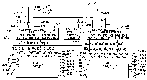
The gate and one side of the drain-source path of logic evaluation pre-
charge transistor 444 are electrically coupled to T5 signal line 436 and the
other
side of the drain-source path is electrically coupled to logic evaluation
signal line
474. The gate of evaluation prevention transistor 442a is electrically coupled
to
T3 signal line 434. The drain-source path of evaluation prevention transistor
442a is electrically coupled on one side to logic evaluation signal line 474
and
on the other side to the reference at 478. The gate of evaluation prevention
transistor 442b is electrically coupled to T4 signal line 422. The drain-
source
path of evaluation prevention transistor 442b is electrically coupled on one
side
to logic evaluation signal line 474 and on the other side to the reference at
478.
The drain-source paths of address transistor pairs 446, 448, ... 470 are
electrically coupled between address lines 472a-472g and evaluation lines
476a-476m. The gates of address transistor pairs 446, 448, ... 470 are driven
CA 02564111 2006-10-18
WO 2005/105455 PCT/US2005/011723
29
by shift register output signals S01-SO13 through shift register output signal
lines 410a-410m.
The gates of address one transistors 446a and 446b are electrically
coupled to shift register output signal line 410a. The drain-source path of
address one transistor 446a is electrically coupled on one side to address
line
472a and on the other side to evaluation line 476a. The drain-source path of
address one transistor 446b is electrically coupled one on side to address
line
472b and on the other side to evaluation line 476a. A high level shift
register
output signal SO1 on shift register output signal line 41 Oa turns on address
one
transistors 446a and 446b as address evaluation transistor 440a is turned on
by
a high voltage level evaluation signal LEVAL on logic evaluation signal line
474.
The address one transistor 446a and address evaluation transistor 440a
conduct to actively pull address line 472a to a low voltage level. The address
one transistor 446b and address evaluation transistor 440a conduct to actively
pull address line 472b to a low voltage level.
The gates of address two transistors 448a and 448b are electrically
coupled to shift register output line 41 Ob. The drain-source path of address
two
transistor 448a is electrically coupled on one side to address line 472a and
on
the other side to evaluation line 476b. The drain-source path of address two
transistor 448b is electrically coupled on one side to address line 472c and
on
the other side to evaluation line 476b. A high level shift register output
signal
S02 on shift register output signal line 410b turns on address two transistors
448a and 448b as address evaluation transistor 440b is turned on by a high
voltage level evaluation signal LEVAL on logic evaluation signal line 474. The
address two transistor 448a and address evaluation transistor 440b conduct to
actively pull address line 472a to a low voltage level. The address two
transistor
448b and address evaluation transistor 440b conduct to actively pull address
line 472c to a low voltage level.
The gates of address three transistors 450a and 450b are electrically
coupled to shift register output signal line 410c. The drain-source path of
address three transistor 450a is electrically coupled on one side to address
line
472a and on the other side to evaluation line 476c. The drain-source path of
CA 02564111 2006-10-18
WO 2005/105455 PCT/US2005/011723
address three transistor 450b is electrically coupled on one side to address
line
472d and on the other side to evaluation line 476c. A high level shift
register
output signal S03 on shift register output signal line 410c turns on address
three transistors 450a and 450b as address evaluation transistor 440c is
turned
5 on by a high voltage level evaluation signal LEVAL on logic evaluation
signal
line 474. The address three transistor 450a and address evaluation transistor
440c conduct to actively pull address line 472a to a low voltage level. The
address three transistor 450b and address evaluation transistor 440c conduct
to
actively pull address line 472d to a low voltage level.
10 The gates of address four transistors 452a and 452b are electrically
coupled to shift register output signal line 410d. The drain-source path of
address four transistor 452a is electrically coupled on one side to address
line
472a and on the other side to evaluation line 476d. The drain-source path of
address four transistor 452b is electrically coupled on one side to address
line
15. 472e and on the other side to evaluation line 476d. A high level shift
register
output signal S04 on shift register output signal line 410d turns on address
four
transistors 452a and 452b as address evaluation transistor 440d is turned on
by
a high voltage level evaluation signal LEVAL on logic evaluation signal line
474.
The address four transistor 452a and address evaluation transistor 440d
20 conduct to actively pull address line 472a to a low voltage level. The
address
four transistor 452b and address evaluation transistor 440d conduct to
actively
pull address line 472e to a low voltage level.
The gates of address five transistors 454a and 454b are electrically
coupled to shift register output signal line 410e. The drain-source path of
25 address five transistor 454a is electrically coupled on one side to address
line
472a and on the other side to evaluation line 476e. The drain-source path of
address five transistor 454b is electrically coupled on one side to address
line
472f and on the other side to evaluation line 476e. A high level shift
register
output signal S05 on shift register output signal line 410e turns on address
five
30 transistors 454a and 454b as address evaluation transistor 440e is turned
on by
a high voltage level evaluation signal LEVAL. The address five transistor 454a
and address evaluation transistor 440e conduct to actively pull address line
CA 02564111 2006-10-18
WO 2005/105455 PCT/US2005/011723
31
472a to a low voltage level. The address five transistor 454b and address
evaluation transistor 440e conduct to actively pull address line 472f to a low
voltage level.
The gates of address six transistors 456a and 456b are electrically
coupled to shift register output signal line 410f. The drain-source path of
address six transistor 456a is electrically coupled on one side to address
line
472a and on the other side to evaluation line 476f. The drain-source path of
address six transistor 456b is electrically coupled on one side to address
line
472g and on the other side to evaluation line 476f. A high level shift
register
output signal S06 on shift register output signal line 41 Of turns on address
six
transistors 456a and 456b to conduct as address evaluation transistor 440f is
turned on by a high voltage level evaluation signal LEVAL. The address six
transistor 456a and address evaluation transistor 440f conduct to actively
pull
address line 472a to a low voltage level. The address six transistor 456b and
address evaluation transistor 440f conduct to actively pull address line 472g
to a
low voltage level.
The gates of address seven transistors 458a and 458b are electrically
coupled to shift register output signal line 410g. The drain-source path of
address six transistor 458a is electrically coupled on one side to address
line
472b and on the other side to evaluation line 476g. The drain source path of
address six transistor 458b is electrically coupled on one side to address
line
472c and on the other side to evaluation line 476g. A high level shift
register
output signal S07 on shift register output signal line 41 Og turns on address
six
transistors 458a and 458b as address evaluation transistor 440g is turned on
by
a high voltage level evaluation signal LEVAL. The address seven transistor
458a and address evaluation transistor 440g conduct to actively pull address
line 472b to a low voltage level. The address seven transistor 458b and
address evaluation transistor 440g conduct to actively pull address line 472c
to
a low voltage level.
The gates of address eight transistors 460a and 460b are electrically
coupled to shift register output signal line 410h. The drain-source path of
address eight transistor 460a is electrically coupled on one side to address
line
CA 02564111 2006-10-18
WO 2005/105455 PCT/US2005/011723
32
472b and on the other side to evaluation line 476h. The drain-source path of
address eight transistor 460b is electrically coupled on one side to address
line
472d and on the other side to evaluation line 476h. A high level shift
register
output signal S08 on shift register output signal line 41 Oh turns on address
eight transistors 460a and 460b as address evaluation transistor 440h is
turned
on by a high voltage level evaluation signal LEVAL. The address eight
transistor 460a and address evaluation transistor 440h conduct to actively
pull
address line 472b to a low voltage level. The address eight transistor 460b
and
address evaluation transistor 440h conduct to actively pull address line 472d
to
a low voltage level.
The gates of address nine transistors 462a and 462b are electrically
coupled to shift register output signal line 4101. The drain-source path of
address nine transistor 462a is electrically coupled on one side to address
line
472b and on the other side to evaluation line 4761. The drain-source path of
address nine transistor 462b is electrically coupled on one side to address
line
472e and on the other side to evaluation line 476i. A high level shift
register
output signal S09 on shift register output signal line 410i turns on address
nine
transistors 462a and 462b to conduct as address evaluation transistor 440i is
turned on by a high voltage level evaluation signal LEVAL. The address nine
transistor 462a and address evaluation transistor 440i conduct to actively
pull
address line 472b to a low voltage level. The address nine transistor 462b and
address evaluation transistor 440i conduct to actively pull address line 472e
to a
low voltage level.
The gates of address ten transistors 464a and 464b are electrically
coupled to shift register output signal line 410j. The drain-source path of
address ten transistor 464a is electrically coupled on one side to address
line
472b and on the other side to evaluation line 476j. The drain-source path of
address ten transistor 464b is electrically coupled on one side to address
line
472f and on the other side to evaluation line 476j. A high level shift
register
output signal SO10 on shift register output signal line 41 Oj turns on address
ten
transistors 464a and 464b as address evaluation transistor 440j is turned on
by
a high voltage level evaluation signal LEVAL. The address ten transistor 464a
CA 02564111 2006-10-18
WO 2005/105455 PCT/US2005/011723
33
and address evaluation transistor 440j conduct to actively pull address line
472b
to a low voltage level. The address ten transistor 464b and address evaluation
transistor 440j conduct to actively pull address line 472f to a low voltage
level.
The gates of address eleven transistors 466a and 466b are electrically
coupled to shift register output signal line 410k. The drain-source path of
address eleven transistor 466a is electrically coupled on one side to address
line 472b and on the other side to evaluation line 476k. The drain-source path
of address eleven transistor 466b is electrically coupled on one side to
address
line 472g and on the other side to evaluation line 476k. A high level shift
register output signal S011 on shift register output signal line 410k turns on
address eleven transistors 466a and 466b as address evaluation transistor 440k
is turned on by a high voltage evaluation signal LEVAL. The address eleven
transistor 466a and address evaluation transistor 440k conduct to actively
pull
address line 472b to a low voltage level. The address eleven transistor 466b
and address evaluation transistor 440k conduct to actively pull address line
472g to a low voltage level.
The gates of address twelve transistors 468a and 468b are electrically
coupled to shift register output signal line 4101. The drain-source path of
address twelve transistor 468a is electrically coupled on one side to address
line
472c and on the other side to evaluation line 4761. The drain-source path of
address twelve transistor 468b is electrically coupled on one side to address
line
472d and on the other side to evaluation line 4761. A high level shift
register
output signal SO12 on shift register output signal line 4101 turns on address
twelve transistors 468a and 468b as address evaluation transistor 4401 is
turned
on by a high voltage level evaluation signal LEVAL. The address twelve
transistor 468a and address evaluation transistor 4401 conduct to actively
pull
address line 472c to a low voltage level. The address twelve transistor 468b
and address evaluation transistor 4401 conduct to actively pull address line
472d
to a low voltage level.
The gates of address thirteen transistors 470a and 470b are electrically
coupled to shift register output signal line 410m. The drain-source path of
address thirteen transistor 470a is electrically coupled on one side to
address
CA 02564111 2006-10-18
WO 2005/105455 PCT/US2005/011723
34
line 472c and on the other side to evaluation line 476m. The drain-source path
of address thirteen transistor 470b is electrically coupled on one side to
address
line 472e and on the other side to evaluation line 476m. A high level shift
register output signal S013 on shift register output signal line 410m turns on
address thirteen transistors 470a and 470b as address evaluation transistor
440m is turned on by a high voltage level evaluation signal LEVAL. The
address thirteen transistor 470a and address evaluation transistor 440m
conduct to actively pull address line 472c to a low voltage level. The address
thirteen transistor 470b and address evaluation transistor 440m conduct to
actively pull address line 472e to a low voltage level.
The shift register 402 shifts a single high voltage level output signal from
one shift register output signal line 410a-410m to the next shift register
output
signal line 410a-410m. Shift register 402 receives a control pulse in control
signal CSYNC on control line 430 and a series of timing pulses from timing
signals T1-T4 to shift the received control pulse into shift register 402. In
response, shift register 402 provides a single high voltage level shift
register
output signal S01 or S013. All of the other shift register output signals S01-
S013 are provided at low voltage levels. Shift register 402 receives another
series of timing pulses from timing signals T1-T4 and shifts the single high
voltage level output signal from one shift register output signal S01-SO13 to
the
next shift register output signal S01-S013, with all other shift register
output
signals S01-SO13 provided at low voltage levels. Shift register 402 receives a
repeating series of timing pulses and in response to each series of timing
pulses, shift register 402 shifts the single high voltage level output signal
to
provide a series of up to thirteen high voltage level shift register output
signals
S01-SO13. Each high voltage level shift register output signal S01-SO13 turns
on two address transistor pairs 446, 448, ... 470 to provide address signals
-Al, -A2, ... -A7 to firing cells 120. The address signals -Al, -A2, ... -A7
are
provided in thirteen address time slots that correspond to the thirteen shift
register output signals S01-SO13. In another embodiment, shift register 402
can include any suitable number of shift register output signals, such as
CA 02564111 2006-10-18
WO 2005/105455 PCT/US2005/011723
fourteen, to provide address signals -Al, -A2, ... -A7 in any suitable number
of
address time slots, such as fourteen address time slots.
The shift register 402 receives direction signals from direction circuit 404
through direction signal lines 408. The direction signals set up the direction
of
5 shifting in shift register 402. The shift register 402 can be set to shift
the high
voltage level output signal in a forward direction, from shift register output
signal
SO1 to shift register output signal SO13, or in a reverse direction, from
shift
register output signal SO 13 to shift register output signal SO1.
In the forward direction, shift register 402 receives the control pulse in
10 control signal CSYNC and provides a high voltage level shift register
output
signal SO1. All other shift register output signals S02-SO1 3 are provided at
low
voltage levels. Shift register 402 receives the next series of timing pulses
and
provides a high voltage level shift register output signal S02, with all other
shift
register output signals SO1 and S03-SO13 provided at low voltage levels. Shift
15 register 402 receives the next series of timing pulses and provides a high
voltage level shift register output signal S03, with all other shift register
output
signals 501, S02, and S04-S013 provided at low voltage levels. Shift register
402 continues to shift the high level output signal in response to each series
of
timing pulses up to and including providing a high voltage level shift
register
20 output signal S013, with all other shift register output signals S01-S012
provided at low voltage levels. After providing the high voltage level shift
register output signal S013, shift register 402 receives the next series of
timing
pulses and provides low voltage level signals for all shift register output
signals
S01-SO13. Another control pulse in control signal CSYNC is provided to start
25 or initiate shift register 402 shifting in the forward direction series of
high voltage
level output signals from shift register output signal S01 to shift register
output
.signal SO13.
In the reverse direction, shift register 402 receives a control pulse in
control signal CSYNC and provides a high level shift register output signal
30 S013. All other shift register output signals S01-SO12 are provided at low
voltage levels. Shift register 402 receives the next series of timing pulses
and
provides a high voltage level shift register output signal SO12, with all
other shift
CA 02564111 2006-10-18
WO 2005/105455 PCT/US2005/011723
36
register output signals SO1-SO11 and S013 provided at low voltage levels.
Shift register 402 receives the next series of timing pulses and provides a
high
voltage level shift register output signal S011, with all other shift register
output
signals S01-SO10, S012 and S013 provided at low voltage levels. Shift
register 402 continues to shift the high voltage level output signal in
response to
each series of timing pulses, up to and including providing a high voltage
level
shift register output signal SO1, with all other shift register output signals
S02-
S013 provided at low voltage levels. After providing the high voltage level
shift
register output signal SO1, shift register 402 receives the next series of
timing
pulses and provides low voltage level signals for all shift register output
signals
S01-S013. Another control pulse in control signal CSYNC is provided to start
or initiate shift register 402 shifting in the reverse direction series of
high voltage
output signals from shift register output signal 5013 to shift register output
signal SO1.
The direction circuit 404 provides two direction signals through direction
signal lines 408. The direction signals set the forward/reverse shifting
direction
in shift register 402. Also, the direction signals can be used to clear the
high
voltage level output signal from shift register 402.
The direction circuit 404 receives a repeating series of timing pulses from
timing signals T3-T6. In addition, direction circuit 404 receives control
pulses in
control signal CSYNC on control line 430. The direction circuit 404 provides
forward direction signals in response to receiving a control pulse coincident
with
a timing pulse from timing signal T4. The forward direction signals set shift
register 402 for shifting in the forward direction from shift register output
signal,,
S01 to shift register output signal S013. The direction circuit 404 provides
reverse direction signals in response to receiving a control pulse coincident
with
a timing pulse from timing signal T6. The reverse direction signals set shift
register 402 for shifting in the reverse direction, from shift register output
signal
SO13 to shift register output signal SO1. Direction circuit 404 provides
direction
signals that clear shift register 402 in response to direction circuit 404
receiving
control pulses coincident with both a timing pulse from timing signal T4 and a
timing pulse from timing signal T6.
CA 02564111 2006-10-18
WO 2005/105455 PCT/US2005/011723
37
The logic array 406 receives shift register output signals SO1-SO13 on
shift register output signal lines 410a-410m and timing pulses from timing
signals T3-T5 on timing signal lines 434, 422 and 436. In response to a single
high voltage level output signal in the shift register output signals S01-SO13
and the timing pulses from timing signals T3-T5, logic array 406 provides two
low voltage level address signals out of the seven address signals -Al, -A2,
...
-A7.
The logic array 406 receives a timing pulse from timing signal T3 that
turns on evaluation prevention transistor 442a to pull the evaluation signal
line
474 to a low voltage level and turn off address evaluation transistors 440.
Also,
the timing pulse from timing signal T3 charges address lines 472a-472g to high
voltage levels through address line pre-charge transistors 438. In one
embodiment, the timing pulse from timing signal T3 is replaced by the timing
pulse from timing signal T4 to charge address lines 472a-472g to high voltage
levels through address line pre-charge transistors 438.
The timing pulse from timing signal T4 turns on evaluation prevention
transistor 442b to pull evaluation signal line 474 to a low voltage level and
turn
off address evaluation transistors 440. The shift register output signals S01-
SO 13 settle to valid output signals during the timing pulse from timing
signal T4.
A single high voltage level output signal in the shift register output signals
S01-
SO 13 is provided to the gates of an address transistor pair 446, 448, ... 470
in
logic array 406. A timing pulse from timing signal T5 charges the evaluation
signal line 474 to a high voltage level to turn on address evaluation
transistors
440. As address evaluation transistors 440 are turned on, an address
transistor
pair 446, 448, ... or 470 in logic array 406 that receive the high voltage
level
shift register output signal SO1-SO13 conduct to discharge the corresponding
address lines 472. The corresponding address lines 472 are actively pulled low
through conducting address transistor pairs 446, 448, ... 470 and a conducting
address evaluation transistor 440. The other address lines 472 remain charged
to a high voltage level.
The logic array 406 provides two low voltage level address signals out of
the seven address signals -Al, -A2, ... -A7 in each address time slot. If
shift
CA 02564111 2006-10-18
WO 2005/105455 PCT/US2005/011723
38
register output signal SO1 is at a high voltage level, address one transistors
446a and 446b conduct to pull address lines 472a and 472b to low voltage
levels and provide active low address signals -Al and -A2. If shift register
output signal S02 is at a high voltage level, address two transistors 448a and
448b conduct to pull address lines 472a and 472c to low voltage levels and
provide active low address signals -Al and -A3. If shift register output
signal
S03 is at a high voltage level, address three transistors 450a and 450b
conduct
to pull address lines 472a and 472d to low voltage levels and provide active
low
address signals -Al and -A4, and so on for each shift register output signal
S04-SO13. The address signals -Al, -A2, ... -A7 for each of the thirteen
address time slots, which correlate to the shift register output signals 801-
S013, are set out in the following table:
Address Time Slot Active address signals
1 -Al and -A2
2 -Al and -A3
3 -Al and -A4
4 -Al and -A5
5 -Al and -A6
6 . -Al and -A7
7 -A2 and -A3
8 -A2 and -A4
9 -A2 and -A5
10 -A2 and-A6
11 -A2 and-A7
12 -A3 and-A4
13 -A3 and-A5
In another embodiment, logic array 406 can provide active address
signals -Al, -A2, ... -A7 for each of thirteen address time slots as set out
in the
following table:
CA 02564111 2006-10-18
WO 2005/105455 PCT/US2005/011723
39
Address Time Slot Active address signals
1 -Al and -A3
2 -Al and -A4
3 -Al and -A5
4 -Al and -A6
-A2 and -A4
6 -A2 and -A5
7 - -A2 and -A6
8 -A2 and -A7
9 -A3 and -A5
-A3 and-A6
11 -A3 and -A7
12 -A4 and-A6
13 -A4 and-A7
Also, in other embodiments, the logic array 406 can include address
transistors that provide any suitable number of low voltage level address
signals
-Al, -A2, ... -A7 for each high voltage level output signal SO1-SO13 and in
5 any suitable sequence of low voltage level address signals -Al, -A2, ... -
A7.
This can be done by, for example, appropriately locating each transistor pair
446, 448, ... 470 to discharge any two desired address lines 672a-g.
In addition, in other embodiments, logic array 406 can include any
suitable number of address lines to provide any suitable number of address
10 signals in any suitable number of address timeslots.
In operation, a repeating series of six timing pulses is provided from
timing signals T1-T6. Each of the timing signals T1-T6 provides one timing
pulse in each series of six timing pulses. The timing pulse from timing signal
T1
is followed by the timing pulse from timing signal T2, followed by the timing
pulse from timing signal T3, followed by the timing pulse from timing signal
T4,
followed by the timing pulse from timing signal T5, which is followed by the
timing pulse from timing signal T6. The series of six timing pulses is
repeated in
the repeating series of six timing pulses.
CA 02564111 2006-10-18
WO 2005/105455 PCT/US2005/011723
In one series of the six timing pulses, direction circuit 404 receives a
timing pulse from timing signal T3 in fourth pre-charge signal PRE4. The
timing
pulse in fourth pre-charge signal PRE4 charges a first one of the direction
lines
408 to a high voltage level. The direction circuit 404 receives a reduced
voltage
5 level timing pulse from timing signal T4 in fourth evaluation signal EVAL4.
If
direction circuit 404 receives a control pulse in control signal CSYNC
coincident
with (at the same time as) the fourth evaluation signal EVAL4, direction
circuit
404 discharges the first direction line 408. If direction 404 receives a low
voltage level control signal CSYNC coincident with the timing pulse in the
fourth
10 evaluation signal EVAL4, the first direction line 408 remains charged to a
high
voltage level.
Next, direction circuit 404 receives a timing pulse from timing signal T5 in
third pre-charge signal PRE3. The timing pulse in third pre-charge signal PRE3
charges a second one of the direction lines 408. The direction circuit 404
15 receives a reduced voltage level timing pulse from timing signal T6 in
third
evaluation signal EVAL3. If the direction circuit 404 receives a control pulse
in
control signal CSYNC coincident with a timing pulse in third evaluation signal
EVAL3, direction circuit 404 discharges the second direction line 408 to a low
voltage level. If direction circuit 404 receives a low voltage level control
signal
20 CSYNC coincident with the timing pulse in third evaluation signal EVAL3,
the
second direction line 408 remains charged to a high voltage level.
If the first direction line 408 is discharged to a low voltage level and the
second direction line 408 remains at a high voltage level, the signal levels
on
the first and second direction lines 408 set up shift register 402 to shift in
the
25 forward direction. If the first direction line 408 remains at a high
voltage level
and the second direction line 408 is discharged to a low voltage level, the
signal
levels on direction lines 408 set up shift register 402 to shift in the
reverse
direction. If both the first and second direction lines 408 are discharged to
low
voltage levels, shift register 402 is prevented from providing a high voltage
level
30 shift register output signal S01-SO13. The direction signals on direction
lines
408 are set during each series of six timing pulses.
CA 02564111 2006-10-18
WO 2005/105455 PCT/US2005/011723
41
To begin, the direction is set in one series of six timing pulses and shift
register 402 is initiated in the next series of six timing pulses. To initiate
shift
register 402, shift register 402 receives a timing pulse from timing signal T1
in
first pre-charge signal PREI. The timing pulse in first pre-charge signal PREI
pre-charges an internal node in each of the thirteen shift register cells,
indicated
at 403a-403m. The shift register 402 receives a reduced voltage level timing
pulse from timing signal T2 in first evaluation signal EVAL1. If a control
pulse in
control signal CSYNC is received by shift register 402 coincident with the
timing
pulse in first evaluation signal EVAL1, shift register 402 discharges the
internal
node of one of the thirteen shift register cells to provide a low voltage
level at
the discharged internal node. If the control signal CSYNC remains at a low
voltage level coincident with the timing pulse in first evaluation signal
EVAL1,
the internal node in each of the thirteen shift register cells remains at a
high
voltage level.
Shift register 402 receives a timing pulse from timing signal T3 in second
pre-charge signal PRE2. The timing pulse in second pre-charge signal PRE2
pre-charges each of the thirteen shift register output lines 410a-410m to
provide
high voltage level shift register output signals S01-SO13. Shift register 402
receives a reduced voltage level timing pulse from timing signal T4 in second
evaluation signal EVAL2. If the internal node in a shift register cell 403 is
at a
low voltage level, such as after receiving the control pulse from control
signal
CSYNC coincident with the timing pulse in first evaluation signal EVAL1, shift
register 402 maintains the shift register output signal SO1-SO13 at the high
voltage level. If the internal node in a shift register cell 403 is at a high
voltage
level, such as in all other shift register cells 403, shift register 402
discharges
the shift register output line 41 Oa-41 Om to provide low voltage level shift
register
output signals S01-SO13. The shift register 402 is initiated in one series of
the
six timing pulses. The shift register output signals S01-SO13 become valid
during the timing pulse from timing signal T4 in second evaluation signal
EVAL2
and remain valid until the timing pulse from timing signal T3 in the next
series of
six timing pulses. In each subsequent series of the six timing pulses, shift
CA 02564111 2006-10-18
WO 2005/105455 PCT/US2005/011723
42
register 402 shifts the high voltage level shift register output signal SO1-
SO13
from one shift register cell 403 to the next shift register cell 403.
The logic array 406 receives the shift register output signals S01-SO13.
In one embodiment, logic array 406 receives the timing pulse from timing
signal
T3 to pre-charge address lines 472 and turn off address evaluation transistors
440. In one embodiment, logic array 406 receives the timing pulse from timing
signal T3 to turn off address evaluation transistors 440 and a timing pulse
from
timing signal T4 to pre-charge address lines 472.
Logic array 406 receives the timing pulse from timing signal T4 to turn off
address evaluation transistors 440 as shift register output signals S01-SO13
settle to valid shift register output signals S01-SO13. If shift register 402
is
initiated, one shift register output signal SO1-SO13 remains at a high voltage
level after the timing pulse from timing signal T4. Logic array 406 receives
the
timing pulse from timing signal T5 to charge evaluation signal line 474 and
turn
on address evaluation transistor 440. The address transistor pair 446, 448,
...
470 that receives the high voltage level shift register output signal S01-SO13
are turned on to pull two of the seven address lines 472a-472g to low voltage
levels. The two low voltage level address signals in address signals -Al, -A2,
... -'A7 are used to enable firing cells 120 and firing cell subgroups for
activation.
The address signals -Al, -'A2, ... -A7 become valid during the timing pulse
from timing signal T5 and remain valid until the timing pulse from timing
signal
T3 in the next series of six timing pulses.
If shift register 402 is not initiated, all shift register output lines 410
are
discharged to provide low voltage level shift register output signals S01-
SO13.
The low voltage level shift register output signals SO1-SO13 turns off address
transistor pairs 446, 448, ... 470 and address lines 472 remain charged to
provide high voltage level address signals -Al, -A2, ... -'A7. The high
voltage
level address signals -Al, -A2, ... '-A7 prevent firing cells 120 and firing
cell
subgroups from being enabled for activation.
While Figure 9 describes one embodiment of an address circuit, other
embodiments employing different logic elements and components may be
utilized. For example, a controller that receives the above described input
CA 02564111 2006-10-18
WO 2005/105455 PCT/US2005/011723
43
signals, e.g. signal T1-T6 and that provides address signals -Al,. -A2, ... -
A7
may be utilized.
Figure I OA is a diagram illustrating one shift register cell 403a in shift
register 402. Shift register 402 includes thirteen shift register cells 403a-
403m
that provide the thirteen shift register output signals S01-SO13. Each shift
register cell 403a-403m provides one of the shift register output signals SO1-
SO13 and each shift register cell 403a-403m is similar to shift register cell
403a.
The thirteen shift register cells 403 are electrically coupled in series to
provide
shifting in the forward and reverse directions. In other embodiments, shift
register 402 can include any suitable number of shift register cells 403 to
provide any suitable number of shift register output signals.
The shift register cell 403a includes a first stage that is an input stage,
indicated with dashed lines at 500, and a second stage that is an output
stage,
indicated with dashed lines at 502. The first stage 500 includes a first pre-
charge transistor 504, a first evaluation transistor 506, a forward input
transistor
508, a reverse input transistor 510, a forward direction transistor 512 and a
reverse direction transistor 514. The second stage 502 includes a second pre-
charge transistor 516, a second evaluation transistor 518 and an internal node
transistor 520.
In the first stage 500, the gate and one side of the drain-source path of
first pre-charge transistor 504 is electrically coupled to timing signal line
432.
The timing signal line 432 provides timing signal T1 to shift register 402 as
first
pre-charge signal PREI. The other side of the drain-source path of first pre-
charge transistor 504 is electrically coupled to one side of the drain-source
path
of first evaluation transistor 506 and the gate of internal node transistor
520
through internal node 522. The internal node 522 provides shift register
internal
node signal SN1 between stages 500 and 502 to the gate of internal node
transistor 520.
The gate of first evaluation transistor 506 is electrically coupled to first
evaluation signal line 420. The first evaluation signal line 420 provides the
reduced voltage level T2 timing signal to shift register 402 as first
evaluation
signal EVAL1. The other side of the drain-source path of first evaluation
CA 02564111 2006-10-18
WO 2005/105455 PCT/US2005/011723
44
transistor 506 is electrically coupled to one side of the drain-source path of
forward input transistor 508 and one side of the drain-source path of reverse
input transistor 510 through internal path 524.
The other side of the drain-source path of forward input transistor 508 is
electrically coupled to one side of the drain-source path of forward direction
transistor 512 at 526, and the other side of the drain-source path of reverse
input transistor 510 is electrically coupled to one side of the drain-source
path of
reverse direction transistor 514 at 528. The drain-source paths of forward
direction transistor 512 and reverse direction transistor 514 are electrically
coupled to a reference, such as ground, at 530.
The gate of the forward direction transistor 512 is electrically coupled to
direction line 408a that receives the forward direction signal DIRF from
direction
circuit 404. The gate of the reverse direction transistor 514 is electrically
coupled to direction line 408b that receives the reverse direction signal DIRR
from direction circuit 404.
In the second stage 502, the gate and one side of the drain-source path
of second pre-charge transistor 516 are electrically coupled to timing signal
line
434. The timing signal line 434 provides timing signal T3 to shift register
402 as
second pre-charge signal PRE2. The other side of the drain-source path of
second pre-charge transistor 516 is electrically coupled to one side of the
drain-
source path of second evaluation transistor 518 and to shift register output
line
410a. The other side of the drain-source path of second evaluation transistor
518 is electrically coupled to one side of the drain-source path of internal
node
transistor 520 at 532. The gate of second evaluation transistor 518 is
electrically coupled to second evaluation signal line 424 to provide the
reduced
voltage level T4 timing signal to shift register 402 as second evaluation
signal
EVAL2. The gate of internal node transistor 520 is electrically coupled to
internal node 522 and the other side of the drain-source path of internal node
transistor 520 is electrically coupled to a reference, such as ground, at 534.
The
gate of the internal node transistor 520 includes a capacitance at 536 for
storing
the shift register cell internal node signal SN1. The shift register output
signal
CA 02564111 2006-10-18
WO 2005/105455 PCT/US2005/011723
line 41 Oa includes a capacitance at 538 for storing the shift register output
signal SO1.
Each shift register cell 403a-403m in the series of thirteen shift register
cells 403 is similar to shift register cell 403a. The gate of the forward
direction
5 transistor 508 in each shift register cell 403a-403m is electrically coupled
to the
control line 430 or one of the shift register output lines 41 Oa-41 01 to
shift in the
forward direction. The gate of the reverse direction transistor 510 in each
shift
register cell 403a-403m is electrically coupled to the control line 430 or one
of
the shift register output lines 410b-410m to shift in the reverse direction.
The
10 shift register output signal lines 410 are electrically coupled to one
forward
transistor 508 and one reverse transistor 510, except for shift register
output
signal lines 410a and 410m. Shift register output signal line 410a is
electrically
coupled to a forward direction transistor 508 in shift register cell 403b, but
not a
reverse direction transistor 510. Shift register output signal line 410m is
15 electrically coupled to a reverse direction transistor 510 in shift
register cell 4031,
but not a forward direction transistor 508.
The shift register cell 403a is the first shift register 403 in the series of
thirteen shift registers 403 as shift register 402 shifts in the forward
direction.
The gate of forward input transistor 508 in shift register cell 403a is
electrically
20 coupled to control signal line 430 to receive control signal CSYNC. The
second
shift register cell 403b includes the gate of the forward input transistor
electrically coupled to shift register output line 410a to receive shift
register
output signal S01. The third shift register cell 403c includes the gate of the
forward input transistor electrically coupled to shift register output line 41
Ob to
25 receive shift register output signal S02. The fourth shift register cell
403d
includes the gate of the forward input transistor electrically coupled to
shift
register output line 41 Oc to receive shift register output signal S03. The
fifth
shift register cell 403e includes the gate of the forward input transistor
electrically coupled to shift register output line 410d to receive shift
register
30 output signal S04. The sixth shift register cell 403f includes the gate of
the
forward input transistor electrically coupled to shift register output line
410e to
receive shift register output signal S05. The seventh shift register cell 403g
CA 02564111 2006-10-18
WO 2005/105455 PCT/US2005/011723
46
includes the gate of the forward input transistor electrically coupled to
shift
register output line 410f to receive shift register output signal 506. The
eighth
shift register cell 403h includes the gate of the forward input transistor
electrically coupled to shift register output line 410g to receive shift
register
output signal 507. The ninth shift register cell 403i includes the gate of the
forward input transistor electrically coupled to shift register output line
410h to
receive shift register output signal S08. The tenth shift register cell 403j
includes the gate of the forward input transistor electrically coupled to
shift
register output line 410i to receive shift register output signal 509. The
eleventh shift register cell 403k includes the gate of the forward input
transistor
electrically coupled to shift register output line 410j to receive shift
register
output signal S010. The twelfth shift register cell 4031 includes the gate of
the
forward input transistor electrically coupled to shift register output line
410k to
receive shift register output signal S011. The thirteenth shift register cell
403m
includes the gate of the forward input transistor electrically coupled to
shift
register output line 4101 to receive shift register output signal S012.
The shift register cell 403a is the last shift register cell 403 in the series
of
thirteen shift register cells 403 as shift register 402 shifts in the reverse
direction. The gate of reverse input transistor 510 in shift register cell
403a is
electrically coupled to the preceding shift register output line 41 Ob to
receive'
shift register output signal 502. The shift register cell 403b includes the
gate of
the reverse input transistor electrically coupled to shift register output
line 410c
to receive shift register output signal 503. The shift register cell 403c
includes
the gate of the reverse input transistor electrically coupled to shift
register output
line 41 Od to receive shift register output signal S04. The shift register
cell 403d
includes the gate of the reverse input transistor electrically coupled to
shift
register output line 410e to receive shift register output signal 505. The
shift
register cell 403e includes the gate of the reverse input transistor
electrically
coupled to shift register output line 41 Of to receive shift register output
signal
S06. The shift register cell 403f includes the gate of the reverse input
transistor
electrically coupled to shift register output line 410g to receive shift
register
output signal S07. The shift register cell 403g includes the gate of the
reverse
CA 02564111 2006-10-18
WO 2005/105455 PCT/US2005/011723
47
input transistor electrically coupled to shift register output line 410h to
receive
shift register output signal S08. The shift register cell 403h includes the
gate of
the reverse input transistor electrically coupled to shift register output
line 410i
to receive shift register output signal S09. The shift register cell 403i
includes
the gate of the reverse input transistor electrically coupled to shift
register output
line 410j to receive shift register output signal S01 0. The shift register
cell 403j
includes the gate of the reverse input transistor electrically coupled to
shift
register output line 410k to receive shift register output signal SO11. The
shift
register cell 403k includes the gate of the reverse input transistor
electrically
coupled to shift register output line 4101 to receive shift register output
signal
SO12. The shift register cell 4031 includes the gate of the reverse input
transistor electrically coupled to shift register output line 410m to receive
shift
register output signal SO13. The shift register cell 403m includes the gate of
the reverse input transistor electrically coupled to control signal line 430
to
receive control signal CSYNC. Shift register output lines 410a-410m are also
electrically coupled to logic array 406.
Shift register 402 receives a control pulse in control signal CSYNC and
provides a single high voltage level output signal. As described above and
described in detail below, the shifting direction of shift register 402 is set
in
response to direction signals DIRF and DIRR, which are generated during
timing pulses in timing signals T3-T6 based on the control signal CSYNC on
control signal line 430. If shift register 402 is shifting in the forward
direction,
shift register 402 sets shift register output line 410a and shift register
output
signal S01 to a high voltage level in response to the control pulse and timing
pulses on timing signals T1-T4. If shift register 402 is shifting in the
reverse
direction, shift register 402 sets shift register output line 410m and shift
register
output signal S013 to a high voltage level in response to the control pulse
and
timing pulses in timing signal T1-T4. The high voltage level output signal S01
or SO13 is shifted through shift register 402 from one shift register cell 403
to
the next shift register cell 403 in response to timing pulses in timing
signals T1-
T4.
CA 02564111 2006-10-18
WO 2005/105455 PCT/US2005/011723
48
The shift register 402 shifts in the control pulse and shifts the single high
level output signal from one shift register cell 403 to the next shift
register cell
403 using two pre-charge operations and two evaluate operations. The first
stage 500 of each shift register cell 403 receives forward direction signal
DIRF
and reverse direction signal DIRR. Also, the first stage 500 of each shift
register
403 receives a forward shift register input signal SIF and a reverse shift
register
input signal SIR. All shift register cells 403 in shift register 402 are set
to shift in
the same direction and at the same time as timing pulses are received in
timing
signals T1-T4.
The first stage 500 of each shift register cell 403 shifts in either the
forward shift register input signal SIF or the reverse shift register input
signal
SIR. The high or low voltage level of the selected shift register input signal
SIF
or SIR is provided as the shift register output signal S01-SO13. The first
stage
500 of each shift register cell 403 pre-charges internal node 522 during a
timing
pulse from timing signal T1 and evaluates the selected shift register input
signal
SIF or SIR during a timing pulse from timing signal T2. The second stage 502
in
each shift register cell 403 pre-charges shift register output lines 410a-410m
during a timing pulse from timing signal T3 and evaluates the internal node
signal SN (e.g., SN1) during a timing pulse from timing signal T4.
The direction signals DIRF and DIRR set the forward/reverse direction of
shifting in shift register cell 403a and all other shift register cells 403 in
shift
register 402. Shift register 402 shifts in the forward direction if forward
direction
signal DIRF is at a high voltage level and reverse direction signal DIRR is at
a
low voltage level. Shift register 402 shifts in the reverse direction if
reverse
direction signal DIRR is at a high voltage level and forward direction signal
DIRF
is at a low voltage level. If both direction signals DIRF and DIRR are at low
voltage levels, shift register 402 does not shift in either direction and all
shift
register output signals SO1-SO13 are cleared to inactive low voltage levels.
In operation of shifting shift register cell 403a in the forward direction,
forward direction signal DIRF is set to a high voltage level and reverse
direction
signal DIRR is set to a low voltage level. The high voltage level forward
direction signal DIRF turns on forward direction transistor 512 and the low
CA 02564111 2006-10-18
WO 2005/105455 PCT/US2005/011723
49
voltage level reverse direction signal DIRR turns off reverse direction
transistor
514. A timing pulse from timing signal T1 is provided to shift register 402 in
first
pre-charge signal PRE1 to charge internal node 522 to a high voltage level
through first pre-charge transistor 504. Next, a timing pulse from timing
signal
T2 is provided to resistor divide network 412 and a reduced voltage level T2
timing pulse is provided to shift register 402 in first evaluation signal
EVAL1.
The timing pulse in first evaluation signal EVALI turns on first evaluation
transistor 506. If the forward shift register input signal SIF is at a high
voltage
level, forward input transistor 508 is turned on and with forward direction
transistor 512 already turned on, internal node 522 is discharged to provide a
low voltage level internal node signal SN1. The internal node 522 is
discharged
through first evaluation transistor 506, forward input transistor 508 and
forward
direction transistor 512. If the forward shift register input signal SIF is at
a low
voltage level, forward input transistor 508 is turned off and internal node
522
remains charged to provide a high voltage level internal node signal SN1.
Reverse shift register input signal SIR controls reverse input transistor 510.
However, reverse direction transistor 514 is turned off such that internal
node
522 cannot be discharged through reverse input transistor 510.
The internal node signal SN1 on internal node 522 controls internal node
transistor 520. A low voltage level internal node signal SN1 turns off
internal
node transistor 520 and a high voltage level internal node signal SN1 turns on
internal node transistor 520.
A timing pulse from timing signal T3 is provided to shift register 402 as
second pre-charge signal PRE2. The timing pulse in second pre-charge signal
PRE2 charges shift register output line 410a to a high voltage level through
second pre-charge transistor 516. Next, a timing pulse from timing signal T4
is
provided to a resistor divide network 414 and a reduced voltage level T4
timing
pulse is provided to shift register 402 as second evaluation signal EVAL2. The
timing pulse in second evaluation signal EVAL2 turns on second evaluation
transistor 518. If internal node transistor 520 is off, shift register output
line
410a remains charged to a high voltage level. If internal node transistor 520
is
on, shift register output line 41 0a is discharged to a low voltage level. The
shift
CA 02564111 2006-10-18
WO 2005/105455 PCT/US2005/011723
register output signal SO1 is the high/low inverse of the internal node signal
SN1, which was the high/low inverse of the forward shift register input signal
SIF. The level of the forward shift register input signal SIF was shifted to
the
shift register output signal SO1.
5 In shift register cell 403a, the forward shift register input signal SIF is
control signal CSYNC on control line 430. To discharge internal node 522 to a
low voltage level, a control pulse in control signal CSYNC is provided at the
same time as a timing pulse in first evaluation signal EVAL1. The control
pulse
in control signal CSYNC that is coincident with the timing pulse from timing
10 signal T2 initiates shift register 402 for shifting in the forward
direction.
In operation of shifting shift register cell 403a in the reverse direction,
forward direction signal DIRF is set to a low voltage level and reverse
direction
signal DIRR is set to a high voltage level. The low voltage level forward
direction signal DIRF turns off forward direction transistor 512 and the high
15 voltage level reverse direction signal DIRR turns on reverse direction
transistor
514. A timing pulse from timing signal T1 is provided in first pre-charge
signal
PRE1 to charge internal node 522 to a high voltage level through first pre-
charge transistor 504. Next, a timing pulse from timing signal T2 is provided
to
resistor divide network 412 and a reduced voltage level T2 timing pulse is
20 provided in first evaluation signal EVAL1. The timing pulse in first
evaluation
signal EVAL1 turns on first evaluation transistor 506. If the reverse shift
register
input signal SIR is at a high voltage level, reverse input transistor 510 is
turned
on, and with reverse direction transistor 514 already turned on, internal node
522 is discharged to provide a low voltage level internal node signal SN1. The
25 internal node 522 is discharged through first evaluation transistor 506,
reverse
input transistor 510 and reverse direction transistor 514. If the reverse
shift
register input signal SIR is at a low voltage level, reverse input transistor
510 is
turned off and internal node 522 remains charged to provide a high voltage
level
internal node signal SN1. Forward shift register input signal SIF controls
30 forward input transistor 508. However, forward direction transistor 512 is
turned
off such that internal node 522 cannot be discharged through forward input
transistor 508.
CA 02564111 2006-10-18
WO 2005/105455 PCT/US2005/011723
51
A timing pulse from timing signal T3 is provided in second pre-charge
signal PRE2. The timing pulse in second pre-charge signal PRE2 charges shift
register output line 410a to a high voltage level through second pre-charge
resistor 516. Next a timing pulse from timing signal T4 is provided to
resistor
divide network 414 and a reduced voltage level T4 timing pulse is provided in
second evaluation signal EVAL2. The timing pulse in second evaluation signal
EVAL2 turns on second evaluation transistor 518. If internal node transistor
520
is off, shift register output line 410a remains charged to a high voltage
level. If
internal node transistor 520 is on, shift register output line 410a is
discharged to
a low voltage level. The shift register output signal S01 is the high/low
inverse
of the internal node signal SN1, which was the high/low inverse of the reverse
shift register input signal SIR. The level of the reverse shift register input
signal
SIR was shifted to the shift register output signal SO1.
In shift register cell 403a, the reverse shift register input signal SIR is
shift
register output signal S02 on shift register output line 410b. In shift
register cell
403m, the reverse shift register input signal SIR is control signal CSYNC on
control line 430. To discharge internal node 522 in shift register cell 403m
to a
low voltage level, a control pulse in control signal CSYNC is provided at the
same time as a timing pulse in the first evaluation signal EVAL1. The control
pulse in control signal CSYNC that is coincident with the timing pulse from
timing signal T2 initiates shift register 402 for shifting in the reverse
direction
from shift register cell 403m toward shift register cell 403a.
In operation of clearing shift register cell 403a and all shift register cells
403 in shift register 402, direction signals DIRF and DIRR are set to low
voltage
levels. A low voltage forward direction signal DIRF turns off forward
direction
transistor 512 and a low voltage level reverse direction signal DIRR turns off
reverse direction transistor 514. A timing pulse from timing signal T1 is
provided
in first pre-charge signal PRE1 to charge internal node 522 and provide a high
voltage level internal node signal SN1. A timing pulse from timing signal T2
is
provided as a reduced voltage level T2 timing pulse in first evaluation signal
EVAL1 to turn on first evaluation transistor 506. Both forward direction
transistor 512 and reverse direction transistor 514 are turned off such that
CA 02564111 2006-10-18
WO 2005/105455 PCT/US2005/011723
52
internal node 522 is not discharged through either forward input transistor
508
or reverse input transistor 510.
The high voltage level internal node signal SN1 turns on internal node
transistor 520. A timing pulse from timing signal T3 is provided in second pre-
charge signal PRE2 to charge shift register output signal line 410a and all
shift
register output signal lines 410. Next, a timing pulse from timing signal T4
is
provided as a reduced voltage level T4 timing pulse in second evaluation
signal
EVAL2 to turn on second evaluation transistor 518. The shift register output
line
410a is discharged through second evaluation transistor 518 and internal node
transistor 520 to provide a low voltage level shift register output signal
S01.
Also, all other shift register output lines 410 are discharged to provide
inactive
low voltage level shift register output signals S02-SO13.
Figure 1 OB is a diagram illustrating direction circuit 404. The direction
circuit 404 includes a forward direction signal circuit 550 and a reverse
direction
signal circuit 552. The forward direction signal circuit 550 includes a third
pre-
charge transistor 554, a third evaluation transistor 556 and a first control
transistor 558. The reverse direction signal circuit 552 includes a fourth pre-
charge transistor 560, a fourth evaluation transistor 562 and a second control
transistor 564.
The gate and one side of the drain-source path of third pre-charge
transistor 554 are electrically coupled to timing signal line 436. The timing
signal line 436 provides timing signal T5 to direction circuit 404 as third
pre-
charge signal PRES. The other side of the drain-source path of third pre-
charge
transistor 554 is electrically coupled to one side of the drain-source path of
third
evaluation transistor 556 through direction signal line 408a. The direction
signal
line 408a provides the forward direction signal DIRF to the gate of the
forward
direction transistor in each shift register cell 403 in shift register 402,
such as the
gate of forward direction transistor 512 in shift register cell 403a. The gate
of
third evaluation transistor 556 is electrically coupled to the third
evaluation
signal line 428 that provides the reduced voltage level T6 timing signal to
direction circuit 404. The other side of the drain-source path of third
evaluation
transistor 556 is electrically coupled to the drain-source path of control
transistor
CA 02564111 2006-10-18
WO 2005/105455 PCT/US2005/011723
53
558 at 566. The drain-source path of control transistor 558 is also
electrically
coupled to a reference, such as ground, at 568. The gate of control transistor
558 is electrically coupled to control line 430 to receive control signal
CSYNC.
The gate and one side of the drain-source path of fourth pre-charge
transistor 560 are electrically coupled to timing signal line 434. The timing
signal line 434 provides timing signal T3 to direction circuit 404 as fourth
pre-
charge signal PRE4. The other side of the drain-source path of fourth pre-
charge transistor 560 is electrically coupled to one side of the drain-source
path
of fourth evaluation transistor 562 through direction signal line 408b. The
direction signal line 408b provides the reverse direction signal DIRR to the
gate
of the reverse direction transistor in each shift register cell 403 in shift
register
402, such as the gate of reverse direction transistor 514 in shift register
cell
403a. The gate of fourth evaluation transistor 562 is electrically coupled to
the
fourth evaluation signal line 424 that provides the reduced voltage level T4
timing signal to direction circuit 404. The other side of the drain-source
path of
fourth evaluation transistor 562 is electrically coupled to the drain-source
path of
control transistor 564 at 570. The drain-source path of control transistor 564
is
also electrically coupled to a reference, such as ground, at 572. The gate of
control transistor 564 is electrically coupled to control line 430 to receive
control
signal CSYNC.
The direction signals DIRF and DIRR set the direction of shifting in shift
register 402. If forward direction signal DIRF is set to a high voltage level
and
reverse direction signal DIRR is set to a low voltage level, forward direction
transistors, such as forward direction transistor 512, are turned on and
reverse
direction transistors, such as reverse direction transistor 514, are turned
off.
Shift register 402 shifts in the forward direction. If forward direction
signal DIRF
is set to a low voltage level and reverse direction signal DIRR is set to a
high
voltage level, forward direction transistors, such as forward direction
transistor
512, are turned off and reverse direction transistors, such as reverse
direction
transistor 514 are turned on. Shift register 402 shifts in the reverse
direction.
The direction signals DIRF and DIRR are set during each series of timing
pulses
from timing signal T3-T6 as shift register 402 actively shifts in either the
forward
CA 02564111 2006-10-18
WO 2005/105455 PCT/US2005/011723
54
or reverse direction. To terminate shifting or prevent shifting of shift
register
402, direction signals DIRE and DIRR are set to low voltage levels. This
clears
the single high voltage level signal from the shift register output signals
SO1-
5013, such that all shift register output signals S01-SO13 are at low voltage
levels. The low voltage level shift register output signals SO1-SO13 turn off
all
address transistor pairs 446, 448, ... 470 and address signals -A1, -A2, ... -
A7
remain at high voltage levels that do not enable firing cells 120.
In operation, timing signal line 434 provides a timing pulse from timing
signal T3 to direction circuit 404 in fourth pre-charge signal PRE4. The
timing
pulse in fourth pre-charge signal PRE4 charges the reverse direction signal
line
408b to a high voltage level. A timing pulse from timing signal T4 is provided
to
the resistor divide network 414 that provides a reduced voltage level T4
timing
pulse to direction circuit 404 in fourth evaluation signal EVAL4. The timing
pulse in fourth evaluation signal EVAL4 turns on fourth evaluation transistor
562. If a control pulse from control signal CSYNC is provided to the gate of
control transistor 564 at the same time as the timing pulse in fourth
evaluation
signal EVAL4 is provided to fourth evaluation transistor 562, the reverse
direction signal line 408b discharges to a low voltage level. If the control
signal
CSYNC remains at a low voltage level as the timing pulse in the fourth
evaluation signal EVAL4 is provided to fourth evaluation transistor 562, the
reverse direction signal line 408b remains charged to a high voltage level.
Timing signal line 436 provides a timing pulse from timing signal T5 to
direction circuit 404 in third pre-charge signal PRES. The timing pulse in
third
pre-charge signal PRE3 charges the forward direction signal line 408a to a
high
voltage level. A timing pulse from timing signal T6 is provided to resistor
divide
network 416 that provides a reduced voltage level T6 timing pulse to direction
circuit 404 in third evaluation circuit EVAL3. The timing pulse in third
evaluation
signal EVAL3 turns on third evaluation transistor 556. If a control pulse from
control signal CSYNC is provided to the gate of control transistor 558 at the
same time as the timing pulse in third evaluation signal EVAL3 is provided to
third evaluation transistor 556, the forward direction signal line 408a
discharges
to a low voltage level. If the control signal CSYNC remains at a low voltage
CA 02564111 2006-10-18
WO 2005/105455 PCT/US2005/011723
level as the timing pulse in the third evaluation signal EVAL3 is provided to
third
evaluation transistor 556, the forward direction signal line 408a remains
charged
to a high voltage level.
Figure 11 is a timing diagram illustrating operation of address generator
5 400 in the forward direction. The timing signals T1-T6 provide a series of
six
repeating pulses. Each of the timing signals T1-T6 provides one pulse in the
series of six pulses.
In one series of six pulses, timing signal T1 at 600 includes timing pulse
602, timing signal T2 at 604 includes timing pulse 606, timing signal T3 at
608
10 includes timing pulse 610, timing signal T4 at 612 includes timing pulse
614,
timing signal T5 at 616 includes timing pulse 618 and timing signal T6 at 620
includes timing pulse 622. The control signal CSYNC at 624 includes control
pulses that set the direction of shifting in shift register 402 and initiate
shift
register 402 for generating address signals -Al, -'A2, ... -A7, indicated at
625.
15 The timing pulse 602 of timing signal T1 at 600 is provided to shift
register 402 in first pre-charge signal PRE1. During timing pulse 602,
internal
node 522, in each of the shift register cells 403a-403m, charges to provide
high
voltage level internal node signals SNI-SN13. All shift register internal node
signals SN, indicated at 626, are set to high voltage levels at 628. The high
20 voltage level internal node signals SN 626 turn on the internal node
transistor
520 in each of the shift register cells 403a-403m. In this example, the series
of
six timing pulses has been provided prior to timing pulse 602 and shift
register
402 has not been initiated, such that all shift register output signals SO,
indicated at 630, are discharged to low voltage levels, indicated at 632 and
all
25 address signals -Al, -A2, ... -A7 at 625 remain at high voltage levels,
indicated
at 633.
The timing pulse 606 of timing signal T2 at 604 is provided to shift
register 402 in first evaluation signal EVAL1. Timing pulse 606 turns on the
first
evaluation transistor 506 in each of the shift register cells 403a-403m. While
30 control signal CSYNC 624 remains at a low voltage level at 634 and all
shift
register output signals SO 630 remain at low voltage levels at 636, forward
input
transistor 508 and reverse input transistor 510 in each of the shift register
cells
CA 02564111 2006-10-18
WO 2005/105455 PCT/US2005/011723
56
403a-403m are off. The non-conducting forward input transistors 508 and non-
conducting reverse input transistors 510 prevent the internal node 522 in each
of the shift register cells 403a-403m from discharging to a low voltage level.
All
shift register internal node signals SN 626 remain at high voltage levels at
638.
The timing pulse 610 of timing signal T3 at 608 is provided to shift
register 402 in second pre-charge signal PRE2, to direction circuit 404 in
fourth
pre-charge signal PRE4 and to address line pre-charge transistors 438 and
evaluation prevention transistor 422a in logic array 406. During timing pulse
610 in second pre-charge signal PRE2, all shift register output signals SO 630
charge to high voltage levels at 640. Also, during timing pulse 610 in fourth
pre-
charge signal PRE4, reverse direction signal DIRR 642 charges to a high
voltage level at 644. In addition, timing pulse 610 charges all address
signals
625 to high voltage levels at 646 and turns on evaluation prevention
transistor
422a to pull logic evaluation signal LEVAL 648 to a low voltage level at 650.
Timing pulse 614 of timing signal T4 at 612 is provided to shift register
402 in second evaluation signal EVAL2, to direction circuit 404 in fourth
evaluation signal EVAL4 and to evaluation prevention transistor 422b in logic
array 406. The timing pulse 614 in second evaluation signal EVAL2 turns on
second evaluation transistor 518 in each of the shift register cells 403a-
403m.
With the internal node signals SN 626 at high voltage levels having turned on
internal node transistor 520 in each of the shift register cells 403a-403m,
all shift
register output signals SO 630 discharge to low voltage levels at 652. Also,
timing pulse 614 in fourth evaluation signal EVAL4 turns on fourth evaluation
transistor 562. A control pulse at 654 of control signal CSYNC 624 turns on
control transistor 564. With fourth evaluation transistor 562 and control
transistor 564 turned on, direction signal DIRR 642 is discharged to a low
voltage level at 656. In addition, timing pulse 614 turns on evaluation
prevention transistor 442b to hold logic evaluation signal LEVAL 648 at a low
voltage level at 658. The low voltage level logic evaluation signal LEVAL 648
turns off address evaluation transistors 440.
Timing pulse 618 of timing signal T5 at 616 is provided to direction circuit
404 in third pre-charge signal PRE3 and to logic evaluation pre-charge
CA 02564111 2006-10-18
WO 2005/105455 PCT/US2005/011723
57
transistor 444 in logic array 406. During timing pulse 618 in third pre-charge
signal PRE3, forward direction signal DIRF 658 charges to a high voltage level
at 660. The high voltage level forward direction signal DIRF 658 turns on
forward direction transistor 512 in each of the shift register cells 403a-403m
to
set up shift register 402 for shifting in the forward direction. Also, during
timing
pulse 618, logic evaluation signal LEVAL 648 charges to a high voltagelevel at
662, which turns on all logic evaluation transistors 440. With all shift
register
output signals SO 630 at low voltage levels, all address transistor pairs 446,
448, ... 470 are turned off and all address signals -Al, -A2, ... -A7 at 625
remain at high voltage levels.
Timing pulse 622 from timing signal T6 at 620 is provided to direction
circuit 404 as third evaluation signal EVAL3. The timing pulse 622 turns on
third
evaluation transistor 556. Since control signal CSYNC 624 remains at a low
voltage level at 664, control transistor 558 turns off and forward direction
signal
DIRF 658 remains at a high voltage level. The high voltage level forward
direction signal DIRF 658 and low voltage level reverse direction signal DIRR
642 set up each of the shift register cells 403a-403m for shifting in the
forward
direction.
In the next series of six timing pulses, timing pulse 666 charges all
internal node signals SN 626 to high voltage levels. Timing pulse 668 turns on
the first evaluation transistor 506 in each of the shift register cells 403a-
403m.
Control signal CSYNC 624 provides a control pulse at 670 to forward input
transistor 508 in shift register cell 403a. With forward direction transistor
512
already turned on, internal node signal SN1 in shift register cell 403a
discharges
to a low voltage level, indicated at 672. The shift register output signals SO
630
are at low voltage levels at 674, which turns off the forward input transistor
in
shift register cells 403b-403m. With the forward input transistors off, each
of the
other internal node signals SN2-SN13 in shift register cells 403b-403m remain
at high voltage levels, indicated at 676.
During timing pulse 678, all shift register output signals SO 630 are
charged to high voltage levels at 680 and reverse direction signal DIRR 642 is
charged to a high voltage level at 682. In addition, during timing pulse 678
all
CA 02564111 2006-10-18
WO 2005/105455 PCT/US2005/011723
58
address signals -Al, -A2, ... -A7 625 are charged to high voltage levels at
684
and logic evaluation signal LEVAL 648 is discharged to a low voltage level at
686. The low voltage level logic evaluation signal LEVAL 648 turns off address
evaluation transistors 440, which prevents address transistor pairs 446, 448,
...
470 from pulling address signals -Al, -A2, ... -A7 625 to low voltage levels.
During timing pulse 688, shift register output signals S02-SO13
discharge to low voltage levels at 690. Shift register output signal SO1
remains
at a high voltage level, indicated at 692, due to internal node signal SN1 at
672
turning off internal node transistor 520 of shift register cell 403a. Also,
timing
pulse 688 turns on second evaluation transistor 562 and control pulse 694
turns
on control transistor 564 to discharge reverse direction signal DIRR 642 to a
low
voltage level at 696. In addition, timing pulse 688 turns on evaluation
prevention transistor 442b to pull logic evaluation signal LEVAL 648 to a low
voltage level at 698 and keep evaluation transistors 440 turned off.
During timing pulse 700 forward direction signal DIRF 658 is maintained
at a high voltage level and logic evaluation signal LEVAL 648 to is charged to
a
high voltage level at 702. The high voltage level logic evaluation signal
LEVAL
648 at 702 turns on evaluation transistors 440. The high level shift register
output signal S01 at 692 turns on address transistor pairs 446a and 446b and
address signals -Al and -A2 at 625 are actively pulled to low voltage levels
at
704. The other shift register output signals S02-SO13 are pulled to low
voltage
levels at 690, such that address transistors 448, 450, ... 470 are turned off
and
address signals -A3--A7 remain at high voltage levels, indicated at 706. The
address signals -Al, -A2, ... -A7 at 625 become valid during timing pulse 700
in timing signal T5 at 616. Timing pulse 708 turns on third evaluation
transistor
556. However, control signal CSYNC 624 is at a low voltage level at 710 and
forward direction signal DIRF 658 remains at a high voltage level at 712.
In the next series of six timing pulses, timing pulse 714 charges all
internal node signals SN 626 to high voltage levels at 716. Timing pulse 718
turns on first evaluation transistor 506 in each of the shift register cells
403a-
403m to allow discharge of node 522, if the forward input signal SIF at each
of
the shift register cells 403a-403m is in a high voltage level. The forward
input
CA 02564111 2006-10-18
WO 2005/105455 PCT/US2005/011723
59
signal SIF at shift register cell 403a is the control signal CSYNC 624, which
is at
a low voltage level at 720. The forward input signal SIF at each of the other
shift register cells 403b-403m is the shift register output signal SO 630 of
the
preceding shift register cell 403. The shift register output signal SO1 is in
a high
voltage level at 692 and is the forward input signal SIF of second shift
register
cell 403b. The shift register output signals S02-SO13 are all at low voltage
levels at 690.
Shift register cells 403a and 403p-403m receive low voltage level forward
input signals SIF that turn off forward input transistor 508 in each of the
shift
register cells 403a and 403c-403m, such that internal node signals SN1 and
SN3-SN13 remain high at 722. Shift register cell 403b receives the high
voltage
level shift register output signal SO1 as a forward input signal SIF that
turns on
the forward input transistor to discharge internal node signal SN2 at 724.
During timing pulse 726 all shift register output signals SO 630 are
charged to high voltage levels at 728 and reverse direction signal DIRR 642 to
a
high voltage level at 730. Also, timing pulse 726 charges all address signals
-Al, -A2, ... -A7 625 toward a high voltage level at 732 and turns on
evaluation
prevention transistor 442a to pull LEVAL 648 to a low voltage level at 734.
The address signals -A1, -A2, ... -A7 625 were valid from the time
address signals -Al and -A2 were pulled low at 704, until all address signals
-Al, -A2, ... -A7 625 are pulled high at 732. The address signals -Al, -A2,
...
-A7 625 are valid during the timing pulse 708 from timing signal T6 at 620 of
the
preceding series of six timing pulses and the timing pulses 714 and 718 from
timing signals T1 at 600 and T2 at 604 of the present series of six timing
pulses.
Timing pulse 736 turns on second evaluation transistor 518 in each of the
shift register cells 403a-403m to evaluate internal node signals SN 626.
Internal
node signals SN1 and SN3-SN13 are at high voltage levels at 722 and
discharge shift register output signals SO1 and S03-SO13 to low voltage levels
at 738. Internal node signal SN2 is at a low voltage level at 724 that turns
off
the internal node transistor of shift register cell 403b and maintains shift
register
output signal S02 at a high voltage level at 740.
CA 02564111 2006-10-18
WO 2005/105455 PCT/US2005/011723
When fourth evaluation transistor 562 is turned on, by timing pulse 736,
and control pulse 742 in CSYNC 624 turns on control transistor 564, reverse
direction signal DIRR 642 discharges to a low voltage level at 744. The
direction signals DIRR 642 and DIRF 658 are set during each series of six
5 timing pulses. In addition, timing pulse 736 turns on evaluation prevention
transistor 442b to maintain LEVAL 648 at a low voltage level at 746.
During timing pulse 748 forward direction signal DIRF 658 is maintained
at a high voltage level at 750 and LEVAL 648 charges to a high voltage level
at
752. The high voltage level logic evaluation signal LEVAL 678 at 752 turns on
10 evaluation transistors 440. The high voltage level shift register output
signal
S02 at 740 turns on address transistors 448a and 448b to pull address signals
-Al and -A3 to low voltage levels at 754. The other address signals -A2 and
-A4---A7 are maintained at high voltage levels at 756.
Timing pulse 758 turns on third evaluation transistor 556. Control signal
15 CSYNC 624 remains at a low voltage level at 760 to turn off control
transistor
558 and maintain forward direction signal DIRF 642 at a high voltage level.
The next series of six timing pulses shifts the high voltage level shift
register output signal S02 to the next shift register cell 403c that provides
a high
voltage level shift register output signal S03. Shifting continues with each
20 series of six timing pulses until each shift register output signal S01-
S013 has
been high once. After shift register output signal SO13 has been high, the
series of high voltage level shift register output signals SO 630 stops. The
shift
register 402 can be initiated again by providing a control pulse in control
signal
CSYNC, such as control pulse 670, coincident with a timing pulse from timing
25 signal T2 at 604.
In forward direction operation, a control pulse in control signal CSYNC
624 is provided coincident with a timing pulse from timing signal T4 at 612 to
set
the direction of shifting to the forward direction. Also, a control pulse from
control signal CSYNC 624 is provided coincident with a timing pulse from
timing
30 signal T2 at 604 to start or initiate the shift register 402 shifting a
high voltage
signal through the shift register output signals S01-SO13.
CA 02564111 2006-10-18
WO 2005/105455 PCT/US2005/011723
61
Figure 12 is a timing diagram illustrating operation of address generator
400 in the reverse direction. The timing signals T1-T6 provide the repeating
series of six pulses. Each of the timing signals T1-T6 provides one pulse in a
series of six pulses. In one series of six pulses, timing signal T1 at 800
includes
timing pulse 802, timing signal T2 at 804 includes timing pulse 806, timing
signal
T3 at 808 includes timing pulse 810, timing signal T4 at 812 includes timing
pulse 814, timing signal T5 at 816 includes timing pulse 818 and timing signal
T6 at 820 includes timing pulse 822. The control signal CSYNC at 824 includes
control pulses that set the direction of shifting in shift register 402 and
initiate
shift register 402 for generating address signals -Al, -A2, ... -A7, indicated
at
825.
The timing pulse 802 is provided to shift register 402 in first pre-charge
signal PREI. During timing pulse 802, internal node 522 in each of the shift
register cells 403a-403m charges to provide corresponding high voltage level
internal node signals SN1-SN13. Shift register internal node signals SN 826
are
set to high voltage levels at 828. The high voltage level internal node
signals
SN 826 turn on the internal node transistors 520 in shift register cells 403.
In
this example, a series of six timing pulses has been provided prior to timing
pulse 802 and without initiating shift register 402, such that all shift
register
output signals SO 830 are discharged to low voltage levels, indicated at 832
and all address signals -Al, -A2, ... -'A7 at 825 remain at high voltage
levels,
indicated at 833.
The timing pulse 806 is provided to shift register 402 in first evaluation
signal EVAL1. Timing pulse 806 turns on the first evaluation transistor 506 in
each of the shift register cells 403a-403m. The control signal CSYNC 824
remains at a low voltage level at 834 and all shift register output signals SO
830
remain at low voltage levels at 836 to turn off the forward input transistor
508
and reverse input transistor 510 in each of the shift register cells 403a-
403m.
The non-conducting forward and reverse input transistors 508 and 510 prevent
the internal node 522 in each of the shift register cells 403a-403m from
discharging to a low voltage level. All shift register internal node signals
SN 826
remain at high voltage levels at 838.
CA 02564111 2006-10-18
WO 2005/105455 PCT/US2005/011723
62
The timing pulse 810 is provided to shift register 402 in second pre-
charge signal PRE2, to direction circuit 404 in fourth pre-charge signal PRE4
and to address line pre-charge transistors 438 and evaluation prevention
transistor 422a in logic array 406. During timing pulse 810, all shift
register
output signals SO 830 are charged to high voltage levels at 840. Also, during
timing pulse 810, reverse direction signal DIRR 842 charges to a high voltage
level at 844. In addition, timing pulse 810 maintains all address signals 825
at
high voltage levels and turns on evaluation prevention transistor 422a to pull
logic evaluation signal LEVAL 848 to a low voltage level at 850.
Timing pulse 814 is provided to shift register 402 in second evaluation
signal EVAL2, to direction circuit 404 in fourth evaluation signal EVAL4 and
to
evaluation prevention transistor 422b in logic array 406. Timing pulse 814
turns
on the second evaluation transistor 518 in each of the shift register cells
403a-
403m. With internal node signals SN 826 at high voltage levels that turn on
internal node transistor 520 in each of the shift register cells 403a-403m,
all shift
register output signals SO 830 discharge to low voltage levels at 852. Also,
timing pulse 814 turns on fourth evaluation transistor 562 and control signal
CSYNC 824 provides a low voltage to turn off control transistor 564. With
control transistor 564 turned off, reverse direction signal DIRR 842 remains
charged to a high voltage level. In addition, timing pulse 814 turns on
evaluation prevention transistor 442b to hold logic evaluation signal LEVAL
848
at a low voltage level at 858. The low voltage level logic evaluation signal
LEVAL 848 turns off address evaluation transistors 440.
Timing pulse 818 is provided to direction circuit 404 in third pre-charge
signal PRE3 and to logic evaluation pre-charge transistor 444 in logic array
406.
During timing pulse 818, forward direction signal DIRF 858 charges to a high
voltage level at 860. Also, during timing pulse 818 logic evaluation signal
LEVAL 848 charges to a high voltage level at 862 to turn on all logic
evaluation
transistors 440. With all shift register output signals SO 830 at low voltage
levels, all address transistor pairs 446, 448, ... 470 are turned off and all
address signals -Al, -A2, ... -A7 at 825 remain at high voltage levels.
CA 02564111 2006-10-18
WO 2005/105455 PCT/US2005/011723
63
Timing pulse 822 is provided to direction circuit 404 as third evaluation
signal EVAL3. The timing pulse 822 turns on third evaluation transistor 556.
The control signal CSYNC 824 provides a control pulse 864 to turn on control
transistor 558 and forward direction signal DIRF 858 is discharged to a low
voltage level at 865. The low voltage level forward direction signal DIRF 858
and high voltage level reverse direction signal DIRR 842 set each of the shift
register cells 403a-403m for shifting in the reverse direction.
In the next series of six timing pulses, during timing pulse 866, all internal
node signals SN 826 are charged to high voltage levels. Timing pulse 868 turns
on the first evaluation transistor 506 in each of the shift register cells
403a-
403m. A control pulse 870, which may be in control signal CSYNC, is provided
to turn on the reverse input transistor in shift register cell 403m and with
the
reverse direction transistor turned on, internal node signal SN13 discharges
to a
low voltage level, indicated at 872. The shift register output signals SO 830
are
at low voltage levels at 874, which turns off the reverse input transistor in
shift
register cells 403a-4031. With the reverse input transistors off, each of the
other
internal node signals SN1-SN12 remain at high voltage levels, indicated at
876.
During timing pulse 878, all shift register output signals SO 830 are
charged to high voltage levels at 880 and reverse direction signal DIRR 842 is
maintained at a high voltage level at 882. In addition, timing pulse 878
maintains all address signals -Al, 'A2, ... -A7 825 at high voltage levels at
884
and pulls logic evaluation signal LEVAL 848 to a low voltage level at 886. The
low voltage level logic evaluation signal LEVAL 848 turns off evaluation
transistors 440, which prevents address transistor pairs 446, 448, ... 470
from
pulling address signals -Al, -A2, ... -A7 825 to low voltage levels.
During timing pulse 888, shift register output signals S01-SO12 are
discharged to low voltage levels at 890. Shift register output signal SO13
remains at a high voltage level, indicated at 892, based on the low voltage
level
internal node signal SN13 at 872 that turns off internal node transistor 520
of
shift register cell 403m. Also, timing pulse 888 turns on second evaluation
transistor and control signal CSYNC 824 turns off control transistor 564 to
maintain reverse direction signal DIRR 842 at a high voltage level at 896. In
CA 02564111 2006-10-18
WO 2005/105455 PCT/US2005/011723
64
addition, timing pulse 888 turns on evaluation prevention transistor 442b to
hold
logic evaluation signal LEVAL 848 at a low voltage level at 898 and keep
evaluation transistors 440 turned off. Shift register output signals SO 830
settle
during timing pulse 888, such that one shift register output signal S013 is at
a
high voltage level and all other shift register output signals S01-SO12 are at
low
voltage levels.
During timing pulse 900, forward direction signal DIRF 858 charges to a
high voltage level at 901 and logic evaluation signal LEVAL 848 charges to a
high voltage level at 902. The high voltage level logic evaluation signal
LEVAL
848 at 902 turns on evaluation transistors 440. The high voltage level shift
register output signal S013 at 892 turns on address transistors 470a and 470b
and address signals -A3 and -A5 are actively pulled to low voltage levels,
indicated at 904. The other shift register output signals S01-SO12 are pulled
to
low voltage levels at 890, such that address transistor pairs 446, 448, ...
468
are turned off and address signals -Al, -A2, -A4, -A6 and -A7 remain at high
voltage levels, indicated at 906. The address signals -Al, -A2, ... -A7 825
become valid during timing pulse 900. Timing pulse 908 turns on third
evaluation transistor 556 and a control pulse 910 in control signal CSYNC 824
turns on control transistor 558 to discharge the forward direction signal DIRF
858 to a low voltage at 912.
In the next series of six timing pulses, during timing pulse 914 all internal
node signals SN 826 are charged to high voltage levels at 916. Timing pulse
918 turns on first evaluation transistor 506 in each of the shift register
cells
403a-403m to discharge node 522 if the reverse input signal SIR at each of the
shift register cells 403a-403m is at a high voltage level. The reverse input
signal
SIR at shift register cell 403m is the control signal CSYNC 824, which is at a
low
voltage level at 920. The reverse input signal SIR at each of the other shift
register cells 403a-4031 is the shift register output signal SO 830 of the
following
shift register cell 403. The shift register output signal S013 is at a high
voltage
level at 892 and is the reverse input signal SIR of shift register cell 4031.
The
shift register output signals SO1-SO12 are all at low voltage levels at 890.
Shift
register cells 403a-403k and 403m have low voltage level reverse input signals
CA 02564111 2006-10-18
WO 2005/105455 PCT/US2005/011723
SIR that turn off reverse input transistor 510, such that internal node
signals
SN1-SN11 and SN13 remain at high voltage levels at 922. Shift register cell
4031 receives the high voltage level shift register output signal S013 as the
reverse input signal SIR that turns on the reverse input transistor to
discharge
5 internal node signal SN12 at 924.
During timing pulse 926, all shift register output signals SO 830 are
charged to high voltage levels at 928 and reverse direction signal DIRR 842 is
maintained at a high voltage level at 930. Also, during timing pulse 926 all
address signals -Al, -A2, ... -A7 825 are charged to a high voltage level at
932
10 and evaluation prevention transistor 442a is turned on to pull LEVAL 848 to
a
low voltage level at 934. The address signals -Al, -A2, ... -A7 825 were valid
from the time address signals -A3 and -A5 were pulled low at 904 until all
address signals -Al, -A2, ... -A7 825 are pulled high at 932. The address
signals -Al, -A2, ... -A7 825 are valid during the timing pulses 908, 914 and
15 918.
Timing pulse 936 turns on second evaluation transistor 518 in each of the
shift register cells 403a-403m to evaluate the internal node signals SN 826.
Internal node signals SN1-SN11 and SN13 are at high voltage levels at 922 to
discharge shift register output signals S01-SO11 and S013 to low voltage
20 levels at 938. Internal node signal SN12 is at a low voltage level at 924
that
turns off the internal node transistor of shift register cell 4031 and
maintains shift
register output signal S012 at a high voltage level at 940.
Also, timing pulse 936 turns on fourth evaluation transistor 562 and
control signal CSYNC 824 is at a low voltage level to turn off control
transistor
25 564 to maintain reverse direction signal DIRR 842 at a high voltage level
at 944.
In addition, timing pulse 936 turns on evaluation prevention transistor 442b
to
maintain LEVAL 848 at a low voltage level at 946.
During timing pulse 948, forward direction signal DIRF 858 is charged to
a high voltage level at 950 and LEVAL 848 is charged to a high voltage level
at
30 952. The high voltage level logic evaluation signal LEVAL 848 at 952 turns
on
evaluation transistors 440. The high voltage level shift register output
signal
S012 at 940 turns on address transistors 468a and 468b to pull address signals
CA 02564111 2006-10-18
WO 2005/105455 PCT/US2005/011723
66
-A3 and -A4 to low voltage levels at 954. The other address signals -Al, -A2
and -A5--'A7 are maintained at high voltage levels at 956.
Timing pulse 958 turns on third evaluation transistor 556. A control pulse
960 in control signal CSYNC 824 turns on control transistor 558 and forward
direction signal DIRF 842 discharges to a low voltage level at 962.
The next series of six timing pulses shifts the high voltage level shift
register output signal S012 to the next shift register cell 403k that provides
a
high voltage level shift register output signal S011. Shifting continues with
each
series of six timing pulses until each shift register output signal S01-SO13
has
been high once. After shift register output signal S01 is high, the series of
high
voltage level shift register output signals SO 830 stops. The shift register
402
can be initiated again by providing a control pulse, such as control pulse
870,
coincident with a timing pulse from timing signal T2 804.
In reverse direction operation, a control pulse from CSYNC 824 is
provided coincident with a timing pulse from timing signal T6 at 820 to set
the
direction of shifting to the reverse direction. Also, a control pulse from
CSYNC
824 is provided coincident with a timing pulse from timing signal T2 804 to
start
or initiate the shift register 402 shifting a high voltage level signal
through the
shift register output signals S01-SO13.
Figure 13 is a block diagram illustrating one embodiment of two address
generators 1000 and 1002 and six fire groups 1004a-1004f. Each of the
address generators 1000 and 1002 is similar to address generator 400 of Figure
9 and fire groups 1004a-1004f are similar to fire groups 202a-202f illustrated
in
Figure 7. The address generator 1000 is electrically coupled to fire groups
1004a-1004c through first address lines 1006. The address lines 1006 provide
address signals -Al, -A2, ... 'A7 from address generator 1000 to each of the
fire groups 1004a-1004c. Also, address generator 1000 is electrically coupled
to control line 1010. Control line 1010 receives conducts control signal CSYNC
to address generator 1000. In one embodiment, the CSYNC signal is provided
by an external controller to a printhead die on which two address generators
1000 and 1002 and six fire groups 1004a-1004f are fabricated. In addition,
address generator 1000 is electrically coupled to select lines 1008a-1008f.
The
CA 02564111 2006-10-18
WO 2005/105455 PCT/US2005/011723
67
select lines 1008a-1 008f are similar to select lines 212a-212f illustrated in
Figure 7. The select lines 1008a-1008f conduct select signals SEL1, SEL2, ...
SEL6 to address generator 1000, as well as to the corresponding fire groups
1004a-1004f (not shown).
The select line 1008a conducts select signal SEL1 to address generator
1000, in one embodiment is timing signal T3 timing signal T6. The select line
1008b conducts select signal SEL2 to address generator 1000, in one
embodiment is timing signal T3 timing signal T1. The select line 1008c
conducts select signal SEL3 to address generator 1000 in one embodiment is
timing signal T3 timing signal T2. The select line 1008d conducts select
signal
SEL4 to address generator 1000, in one embodiment is timing signal T3 timing
signal T3. The select line 1008e conducts select signal SEL5 to address
generator 1000, in one embodiment is timing signal T3 timing signal T4, and
the
select line 1008f conducts select signal SEL6 to address generator 1000, in
one
embodiment is timing signal T3 timing signal T5.
The address generator 1002 is electrically coupled to fire groups 1004d-
1004f through second address lines 1012. The address lines 1012 provide
address signals -131, -B2, ... -137 from address generator 1002 to each of the
fire groups 1004d-1004f. Also, address generator 1002 is electrically coupled
to
control line 1010 that conducts control signal CSYNC to address generator
1002. In addition, address generator 1002 is electrically coupled to select
lines
1008a-1008f. The select lines 1008a-1008f conduct select signals SEL1, SEL2,
... SEL6 to address generator 1002, as well as to the corresponding fire
groups
1004a-1004f (not shown).
The select line 1008a conducts select signal SEL1 to address generator
1002, which in one embodiment is timing signal T3. The select line 1008b
conducts select signal SEL2 to address generator 1002 , which in one
embodiment is timing signal T4. The select line 1008c conducts select signal
SEL3 to address generator 1002, which in one embodiment is timing signal T5.
The select line 1008d conducts select signal SEL4 to address generator 1002,
which in one embodiment is timing signal T6. The select line 1008e conducts
select signal SEL5 to address generator 1002, which in one embodiment is
CA 02564111 2006-10-18
WO 2005/105455 PCT/US2005/011723
68
timing signal T1, and the select line 1008f conducts select signal SEL6 to
address generator 1002, which in one embodiment is timing signal T2.
The select signals SEL1, SEL2, ... SEL 6 include a series of six pulses
that repeats in a repeating series of six pulses. Each of the select signals
SEL1,
SEL2, ... SEL6 includes one pulse in the series of six pulses. In one
embodiment, a pulse in select signal SEL1 is followed by a pulse in select
signal
SEL2, that is followed by a pulse in select signal SEL3, that is followed by a
pulse in select signal SEL4, that is followed by a pulse in select signal
SEL5,
that is followed by a pulse in select signal SEL6. After the pulse in select
signal
SEL6, the series repeats beginning with a pulse in select signal SEL1. The
control signal CSYNC includes pulses coincident with pulses in select signals
SEL1, SEL2, ... SEL6 to initiate address generators 1000 and 1002 and to set
up the direction of shifting or address generation in address generators 1000
and 1002, for example as discussed with respect to Figures 11 and 12. To
initiate address generation from address generator 1000, control signal CSYNC
includes a control pulse coincident with a timing pulse in timing signal T2
that
corresponds to the timing pulse in select signal SEL3.
The address generator 1000 generates address signals -Al, -A2, ... -A7
in response to select signals SEL1, SEL2, ... SEL6 and control signal CSYNC.
The address signals -Al, -A2, ... -A7 are provided through first address lines
1006 to fire groups 1004a-1004c.
In address generator 1000, address signals -Al, -A2, ... -A7 are valid
during timing pulses in timing signals T6, T1 and T2 that correspond to timing
pulses in select signals SEL1, SEL2 and SEL3. The control signal CSYNC
includes a control pulse coincident with a timing pulse in timing signal T4
that
corresponds to the timing pulse in select signal SEL5 to set up address
generator 1000 for shifting in the forward direction. The control signal CSYNC
includes a control pulse coincident with a timing pulse in timing signal T6
that
corresponds to the timing pulse in select signal SEL1 to set up address
generator 1000 for shifting in the reverse direction.
The fire groups 1004a-1004c receive valid address signals -Al, -A2, ...
-A7 during the pulses in select signals SEL1, SEL2 and SEL3. When fire group
CA 02564111 2006-10-18
WO 2005/105455 PCT/US2005/011723
69
one (FG1) at 1004a receives the address signals -Al, -A2, ... -A7 and the
pulse in select signal SEL1, firing cells 120 in selected row subgroups SG1
are
enabled for activation by fire signal FIRE1. When fire group two (FG2) at
1004b
receives the address signals -Al, -A2, ... -A7 and the pulse in select signal
SEL2, firing cells 120 in selected row subgroups SG2 are enabled for
activation
by fire signal FIRE2. When fire group three (FG3) at 1004c receives the
address
signals -Al, -A2, ... -A7 and the pulse in select signal SEL3, firing cells
120 in
selected row subgroups SG3 are enabled for activation by fire signal FIRE3.
The address generator 1002 generates address signals -B1, -B2, ... -B7
in response to the select signals SEL1, SEL2, ... SEL6 and control signal
CSYNC. The address signals -B1, -B2, ... -B7 are provided through second
address lines 1012 to fire groups 1004d-1004f. In address generator 1002, the
address signals -B1, -B2, ... -B7 are valid during timing pulses in timing
signals
T6, T1 and T2 that correspond to timing pulses in select signals SEL4, SEL5
and SEL6. The control signal CSYNC includes a control pulse coincident with a
timing pulse in timing signal T4 that corresponds to the timing pulse in
select
signal SEL2 to set up address generator 1002 for shifting in the forward
direction. The control signal CSYNC includes a control pulse coincident with a
timing pulse in timing signal T6 that corresponds to the timing pulse in
select
signal SEL4 to set up address generator 1002 for shifting in the reverse
direction. To initiate address generation from address generator 1002, control
signal CSYNC includes a control pulse coincident with a timing pulse in timing
signal T2 that corresponds to the timing pulse in select signal SEL6.
The fire groups 1004d-1004f receive valid address signals -81, -B2, ...
-B7 during the pulses in select signals SEL4, SEL5 and SEL6. When fire group
four (FG4) at 1004d receives the address signals -B1, -B2, ... -B7 and the
pulse in select signal SEL4, firing cells 120 in selected row subgroups SG4
are
enabled for activation by fire signal FIRE4. When fire group five (FG5) at
1004e
receives the address signals -B1, -B2, ... -B7 and the pulse in select signal
SEL5, firing cells 120 in selected row subgroups SG5 are enabled for
activation
by fire signal FIRES. When fire group six (FG6) at 1004f receives the address
CA 02564111 2006-10-18
WO 2005/105455 PCT/US2005/011723
signals -B1, -B2, ... -B7 and the pulse in select signal SEL6, firing cells
120 in
selected row subgroups SG6 are enabled for activation by fire signal FIRE6.
In one example operation, during one series of six pulses, control signal
CSYNC includes control pulses coincident with the timing pulses in select
5 signals SEL2 and SEL5 to set up address generators 1000 and 1002 for
shifting
in the forward direction. The control pulse coincident with the timing pulse
in
select signal SEL2 sets up address generator 1002 for shifting in the forward
direction. The control pulse coincident with the timing pulse in select signal
SEL5 sets up address generator 1000 for shifting in the forward direction.
10 In the next series of six pulses, control signal CSYNC includes control
pulses coincident with timing pulses in select signals SEL2, SEL3, SEL5 and
SEL6. The control pulses coincident with timing pulses in select signals SEL2
and SEL5 set the direction of shifting to the forward direction in address
generators 1000 and 1002. The control pulses coincident with timing pulses in
15 select signals SEL3 and SEL6 initiate the address generators 1000 and 1002
for generating address signals -Al, -A2, ... -A7 and -B1, -B2, ... -B7. The
control pulse coincident with the timing pulse in select signal SEL3 initiates
the
address generator 1000 and the control pulse coincident with the timing pulse
in
select signal SEL6 initiates the address generator 1002.
20 During the third series of timing pulses, address generator 1000
generates address signals -Al, -A2, ... -A7 that are valid during timing
pulses
in select signals SEL1, SEL2 and SEL3. The valid address signals -Al, -A2, ...
-A7 are used for enabling firing cells 120 in row subgroups SG1, SG2 and SG3
in fire groups FG1, FG2 and FG3 at 1004a-1004c for activation. During the
third
25 series of timing pulses, address generator 1002 generates address signals -
B1,
-B2, ... -B7 that are valid during timing pulses in select signals SEL4, SEL5
and
SEL6. The valid address signals -B1, -B2, ... -B7 are used for enabling firing
cells 120 in row subgroups SG4, SG5 and SG6 in fire groups FG4, FG5 and
FG6 at 1004d-1004f for activation.
30 During the third series of timing pulses in select signals SEL1, SEL2, ...
SEL6, address signals -Al, -A2, ... -A7 include low voltage level signals that
correspond to one of thirteen addresses and address signals -B1, -B2, ... -B7
CA 02564111 2006-10-18
WO 2005/105455 PCT/US2005/011723
71
include low voltage level signals that correspond to the same one of thirteen
addresses. During each subsequent series of timing pulses from select signals
SEL1, SEL2, ... SEL6, address signals -Al, -A2, ... -A7 and address signals
-B1, -B2, ... -B7 include low voltage level signals that correspond to the
same
one of thirteen addresses. Each series of timing pulses is an address time
slot,
such that one of the thirteen addresses is provided during each series of
timing
pulses.
In forward direction operation, address one is provided first by address
generators 1000 and 1002, followed by address two and so on through address
thirteen. After address thirteen, address generators 1000 and 1002 provide all
high voltage level address signals -Al, -A2, ... -A7 and -B1, -B2, ... -B7.
Also, during each series of timing pulses from select signals SEL1, SEL2 ,...
SEL6, control pulses are provided coincident with timing pulses in select
signals
SEL2 and SEL5 to continue shifting in the forward direction.
In another example operation, during one series of six pulses, control
signal CSYNC includes control pulses coincident with timing pulses in select
signals SEL1 and SEL4 to set up address generators 1000 and 1002 for shifting
in the reverse direction. The control pulse coincident with the timing pulse
in
select signal SEL1 sets up address generator 1000 for shifting in the reverse
direction. The control pulse coincident with the timing pulse in select signal
SEL4 sets up address generator 1002 for shifting in the reverse direction.
In the next series of six pulses, control signal CSYNC includes control
pulses coincident with the timing pulses in select signals SEL1, SEL3, SEL4
and
SEL6. The control pulses coincident with timing pulses in select signals SEL1
and SEL4 set the direction of shifting to the reverse direction in address
generators 1000 and 1002. The control pulses coincident with timing pulses in
select signals SEL3 and SEL6 initiate the address generators 1000 and 1002
for generating address signals -Al, -A2, ... -A7 and -B1, '-B2, ... -B7. The
control pulses coincident with the timing pulse in select signal SEL3
initiates
address generator 1000 and the control pulse coincident with the timing pulse
in
select signal SEL6 initiates address generator 1002.
CA 02564111 2006-10-18
WO 2005/105455 PCT/US2005/011723
72
During the third series of timing pulses, address generator 1000
generates address signals -Al, -A2, ... -A7 that are valid during timing
pulses
in select signals SEL1, SEL2 and SEL3. The valid address signals -Al, -A2, ...
-A7 are used for enabling firing cells 120 in row subgroups SG1, SG2 and SG3
in fire groups FG1, FG2 and FG3 at 1004a-1004c for activation. Address
generator 1002 generates address signals -B1, -B2, ... -B7 that are valid
during timing pulses in select signals SEL4, SEL5 and.SEL6 during the third
series of timing pulses. The valid address signals -B1, -B2, ... -B7 are used
for enabling firing cells 120 in row subgroups SG4, SG5 and SG6 in fire groups
FG4, FG5 and FG6 at 1004d-1004f for activation.
During the third series of timing pulses in select signals SEL1, SEL2, ...
SEL6 in reverse direction operation, address signals -Al, -A2, ... -A7 include
low voltage level signals that correspond to one of thirteen addresses and
address signals -B1, -B2, ... -B7 include low voltage level signals that
correspond to the same one of thirteen addresses. During each subsequent
series of timing pulses from select signals SEL1, SEL2, ... SEL6, address
signals -Al, -A2, ... -A7 and -B1, -B2, ... -B7 include low voltage level
signals
that correspond to the same one of thirteen addresses. Each series of timing
pulses is an address time slot, such that one of the thirteen addresses is
provided during each series of timing pulses.
In reverse direction operation, address thirteen is provided first by
address generator 1000 and 1002, followed by address twelve and so on
through address one. After address one, address generators 1000 and 1002
provide all high voltage level address signals -Al, -A2, ... -A7 and -B1, -B2,
...
-B7. Also, during each series of timing pulses from select signals SEL1, SEL2
... SEL6 control pulses are provided coincident with timing pulses in select
signals SEL1 and SEL4 to continue shifting in the reverse direction.
To terminate or prevent address generation, control signal CSYNC
includes control pulses coincident with timing pulses in select signals SEL1,
SEL2, SEL4 and SEL5. This clears the shift registers, such as shift register
402, in address generators 1000 and 1002. A constant high voltage level, or a
series of high voltage pulses, in control signal CSYNC also terminates or
CA 02564111 2006-10-18
WO 2005/105455 PCT/US2005/011723
73
prevents address generation and a constant low voltage level in control signal
CSYNC will not initiate address generators 1000 and 1002.
Figure 14 is a timing diagram illustrating forward and reverse operation of
address generators 1000 and 1002. The control signal used for shifting in the
forward direction is CSYNC(FWD) at 1124 and the control signal used for
shifting in the reverse direction is CSYNC(REV) at 1126. The address signals
-Al, -A2, ... -A7 at 1128 are provided by address generator 1000 and include
both forward and reverse operation address references. The address signals
-B1, -B2, ... -B7 at 1130 are provided by address generator 1002 and include
both forward and reverse operation address references.
The select signals SEL1, SEL2, ... SEL6 provide a repeating series of six
pulses. Each of the select signals SEL1, SEL2, SEL6 includes one pulse in the
series of six pulses. In one series of the repeating series of six pulses,
select
signal SEL1 at 1100 includes timing pulse 1102, select signal SEL2 at 1104
includes timing pulse 1106, select signal SEL3 at 1108 includes timing pulse
1110, select signal SEL4 at 1112 includes timing pulse 1114, select signal
SEL5
at 1116 includes timing pulse 1118 and select signal SEL6 at 1120 includes
timing pulse 1122.
In forward direction operation, control signal CSYNC(FWD) 1124
includes control pulse 1132 coincident with timing pulse 1106 in select signal
SEL2 at 1104. The control pulse 1132 sets up address generator 1002 for
shifting in the forward direction. Also, control signal CSYNC(FWD) 1124
includes control pulse 1134 coincident with timing pulse 1118 in select signal
SEL5 at 1116. The control pulse 1134 sets up address generator 1000 for
shifting in the forward direction.
In the next repeating series of six pulses, the select signal SEL1 at 1100
includes timing pulse 1136, select signal SEL2 at 1104 includes timing pulse
1138, select signal SEL3 at 1108 includes timing pulse 1140, select signal
SEL4
at 1112 includes timing pulse 1142, select signal SEL5 at 1116 includes timing
pulse 1144 and select signal SEL6 at 1120 includes timing pulse 1146.
Control signal CSYNC(FWD) 1124 includes control pulse 1148 coincident
with timing pulse 1138 to continue setting address generator 1002 for shifting
in
CA 02564111 2006-10-18
WO 2005/105455 PCT/US2005/011723
74
the forward direction and control pulse 1152 coincident with timing pulse 1144
to continue setting address generator 1000 for shifting in the forward
direction.
Also, control signal CSYNC(FWD) 1124 includes control pulse 1150 coincident
with timing pulse 1140 in select signal SEL3 at 1108. The control pulse 1150
initiates address generator 1000 for generating address signals -Al, -A2, ...
-A7 at 1128. In addition, control signal CSYNC(FWD) 1124 includes control
pulse 1154 coincident with timing pulse 1146 in select signal SEL6 at 1120.
The control pulse 1154 initiates address generator 1002 for generating address
signals -B1, -B2, ... -B7 at 1130.
In the next or third series of six pulses, select signal SEL1 at 1100
includes timing pulse 1156, select signal SEL2 at 1104 includes timing pulse
1158, select signal SEL3 at 1108 includes timing pulse 1160, select signal
SEL4
at 1112 includes timing pulse 1162, select signal SEL5 at 1116 includes timing
pulse 1164 and select signal SEL6 at 1120 includes timing pulse 1166. The
control signal CSYNC(FWD) 1124 includes control pulse 1168 coincident with
timing pulse 1158 to continue setting address generator 1002 for shifting in
the
forward direction and control pulse 1170 coincident with timing pulse 1164 to
continue setting address generator 1000 for shifting in the forward direction.
The address generator 1000 provides address signals -Al, -A2, ... -A7
at 1128. After being initiated in forward direction operation, address
generator
1000 and address signals -Al, -A2, ... -A7 at 1128 provide address one at
1172. Address one at 1172 becomes valid during timing pulse 1146 in select
signal SEL6 at 1120 and remains valid until timing pulse 1162 in select signal
SEL4 at 1112. Address one at 1172 is valid during timing pulses 1156, 1158
and 1160 in select signals SEL1, SEL2 and SEL3 at 1100, 1104 and 1108.
The address generator 1002 provides address signals -B1, -B2, ... -B7
at 1130. After being initiated in forward direction operation, address
generator
1002 and address signals -B1, -B2, ... -B7 at 1130 provide address one at
1174. Address one at 1174 becomes valid during timing pulse 1160 in select
signal SEL3 at 1108 and remains valid until timing pulse 1176 in select signal
SEL1 at 1100. Address one at 1174 is valid during timing pulses 1162, 1164
and 1166 in select signals SEL4, SEL5 and SEL6 at 1112, 1116 and 1120.
CA 02564111 2006-10-18
WO 2005/105455 PCT/US2005/011723
The address signals -Al, -A2, ... -A7 at 1128 and -B1, -B2, ... -B7 at
1130 provide the same address, address one at 1172 and 1174. Address one
is provided during the series of six timing pulses beginning with timing pulse
1156 and ending with timing pulse 1166, which is the address time slot for
5 address one. During the next series of six pulses, beginning with timing
pulse
1176, address signals -Al, -A2, ... -A7 at 1128 provide address two at 1178
and address signals -B1, -B2, ... -B7 at 1130 provide address two also. In
this way, address generators 1000 and 1002 provide addresses from address
one through address thirteen in the forward direction. After address thirteen,
10 address generators 1000 and 1002 are reinitiated to cycle through the valid
addresses again in the same way.
In reverse direction operation, control signal CSYNC(REV) 1126 includes
control pulse 1180 coincident with timing pulse 1102 in select signal SEL1 at
1100. The control pulse 1180 sets up address generator 1000 for shifting in
the
15 reverse direction. Also, control signal CSYNC(REV) 1126 includes control
pulse
1182 coincident with timing pulse 1114 in select signal SEL4 at 1112. The
control pulse 1182 sets up address generator 1002 for shifting in the reverse
direction.
Control signal CSYNC(REV) 1126 includes control pulse 1184 coincident
20 with timing pulse 1136 to continue setting address generator 1000 for
shifting in
the reverse direction and control pulse 1188 coincident with timing pulse 1142
to continue setting address generator 1002 for shifting in the reverse
direction.
Also, control signal CSYNC(REV) 1126 includes control pulse 1186 coincident
with timing pulse 1140 in select signal SEL3 at 1108. The control pulse 1186
25 initiates address generator 1000 for generating address signals -Al, -A2,
...
-A7 at 1128. In addition, control signal CSYNC(REV) 1126 includes control
pulse 1190 coincident with timing pulse 1146 in select signal SEL6 at 1120.
The control pulse 1190 initiates address generator 1002 for generating address
signals -B1, -B2, ... -B7 at 1130.
30 The control signal CSYNC(REV) 1126 includes control pulse 1192
coincident with timing pulse 1156 to continue setting address generator 1000
for
shifting in the reverse direction and control pulse 1194 coincident with
timing
CA 02564111 2006-10-18
WO 2005/105455 PCT/US2005/011723
76
i
pulse 1162 to continue setting address generator 1002 for shifting in the
reverse
direction.
The address generator 1000 provides address signals -A1-A7 at 1128.
After being initiated in reverse direction operation, address generator 1000
and
address signals -Al, -A2, ... -A7 at 1128 provide address thirteen at 1172.
Address thirteen at 1172 becomes valid during timing pulse 1146 and remains
valid until timing pulse 1162. Address thirteen at 1172 is valid during timing
pulses 1156, 1158 and 1160 in select signals SEL1, SEL2 and SEL3 at 1100,
1104 and 1108.
The address generator 1002 provides address signals -B1, -B2, ... -B7
at 1130. After being initiated in reverse direction operation, address
generator
1002 and address signals -B1, -B2, ... -B7 at 1130 provide address thirteen at
1174. Address thirteen at 1174 becomes valid during timing pulse 1160 and
remains valid until timing pulse 1176. Address thirteen at 1174 is valid
during
timing pulses 1162, 1164 and 1166 in select signals SEL4, SEL5 and SEL6 at
1112, 1116 and 1120.
The address signals -Al, -A2, ... -A7 at 1128 and -B1, -B2, ... -B7 at
1130 provide the same address, address thirteen at 1172 and 1174. Address
thirteen is provided during the series of six timing pulses beginning with
timing
pulse 1156 and ending with timing pulse 1166, which is the address time slot
for
address thirteen. During the next series of six pulses, beginning with timing
pulse 1176, address signals -Al, -A2, ... -A7 at 1128 provide address twelve
at 1178 and address signals -B1, -B2, ... -B7 at 1130 provide address twelve
also. Address generators 1000 and 1002 provide addresses from address
thirteen through address one in the reverse direction. After address one,
address generators 1000 and 1002 are reinitiated to provide valid addresses
again.
Figure 15 is a diagram illustrating one embodiment of a bank select
address generator 1200 in a printhead die 40. The bank select address
generator 1200 is one embodiment of control circuitry in printhead die 40. The
bank select address generator 1200 is configured to provide twenty six address
signal combinations, referred to as addresses 1-26, in eight address signals
CA 02564111 2006-10-18
WO 2005/105455 PCT/US2005/011723
77
-Al, -A2 ... ~A8. Lower number addresses 1-13, referred to as lower bank
addresses 1-13, are provided to enable firing cells in a first group of firing
cells,
referred to as the lower bank of firing cells. Higher number addresses 14-26,
referred to as higher bank addresses 14-26, are provided to enable firing
cells in
a second group of firing cells, referred to as the higher bank of firing
cells. In
one embodiment, two of eight address signals -Al, -A2 ... -A8 are active at a
time to provide twenty six addresses 1-26.
The bank select address generator 1200 includes a lower bank shift
register 1202, a higher bank shift register 1204, a lower bank logic circuit
1206,
a higher bank logic circuit 1208 and a direction circuit 1210. The lower bank
shift register 1202 is similar to shift register 402 (shown in Figure 9) and,
also,
higher bank shift register 1204 is similar to shift register 402. The lower
bank
shift register 1202 receives different timing signals than shift register 402
and
higher bank shift register 1204 receives different timing signals than shift
register 402. The lower bank logic circuit 1206 includes transistor logic,
similar
to logic circuit 406 (shown in Figure 9), to provide lower bank addresses 1-13
and the higher bank logic circuit 1208 includes transistor logic, similar to
logic
circuit 406, to provide higher bank addresses 14-26.
The lower bank shift register 1202 is electrically coupled to lower bank
logic circuit 1206 through shift register output lines 1212a-1212m. The shift
register output lines 1212a-1212m provide shift register output signals S01-
S013 to logic circuit 1206 as logic circuit input signals All-AI13,
respectively.
Also, lower bank shift register 1202 is electrically coupled to control signal
line
1214 that provides control signal CSYNC to lower bank shift register 1202. In
addition, lower bank shift register 1202 receives timing pulses in bank timing
signals BT1, BT4, BT5 and BT6.
Lower bank shift register 1202 is electrically coupled to timing signal line
1216 that provides bank timing signal BT6 to lower bank shift register 1202 as
first pre-charge signal PRE1. Lower bank shift register 1202 is electrically
coupled to first resistor divide network 1218 through first evaluation signal
line
1220. The first resistor divide network 1218 is electrically coupled to timing
signal line 1222 that provides bank timing signal BT1 to first resistor divide
CA 02564111 2006-10-18
WO 2005/105455 PCT/US2005/011723
78
network 1218. The first resistor divide network 1218 provides a reduced
voltage
level BT1 timing signal to lower bank shift register 1202 on first evaluation
signal
line 1220 as first evaluation signal EVALI. Lower bank shift register 1202 'is
electrically coupled to timing signal line 1224 that provides bank timing
signal
BT4 to lower bank shift register 1202 as second pre-charge signal PRE2 and
lower bank shift register 1202 is electrically coupled to second resistor
divide
network 1226 through second evaluation signal line 1228. The second resistor
divide network 1226 is electrically coupled to timing signal line 1230 that
provides bank timing signal BT5 to second resistor divide network 1226. The
second resistor divide network 1226 provides a reduced voltage level BT5
timing signal to lower bank shift register 1202 through second evaluation
signal
line 1228 as second evaluation signal EVAL2.
The higher bank shift register 1204 is electrically coupled to higher bank
logic circuit 1208 through shift register output lines 1232a-1232m. The shift
register output lines 1232a-1232m provide shift register output signals SO1-
S013 to logic circuit 1208 as logic circuit input signals A114-AI26,
respectively.
Also, higher bank shift register 1204 is electrically coupled to control
signal line
1214 that provides control signal CSYNC to higher bank shift register 1204. In
addition, higher bank shift register 1204 receives timing pulses in timing
signals
BT3, BT4, BT5 and BT6.
Higher bank shift register 1204 is electrically coupled to timing signal line
1216 that provides bank timing signal BT6 to higher bank shift register 1204
as
first pre-charge signal PRE1. Higher bank shift register 1204 is electrically
coupled to third resistor divide network 1227 through first evaluation signal
line
1221. The third resistor divide network 1227 is electrically coupled to timing
signal line 1229 that provides bank timing signal BT3 to third resistor divide
network 1227. The third resistor divide network 1227 provides a reduced
voltage level BT3 timing signal to higher bank shift register 1204 through
first
evaluation signal line 1221 as first evaluation signal EVAL1. Higher bank
shift
register 1204 is electrically coupled to timing signal line 1224 that provides
bank
timing signal BT4 to higher bank shift register 1204 as second pre-charge
signal
PRE2. Higher bank shift register 1204 is electrically coupled to second
CA 02564111 2006-10-18
WO 2005/105455 PCT/US2005/011723
79
evaluation signal line 1228 that provides a reduced voltage level BT5 timing
signal to higher bank shift register 1204 as second evaluation signal EVAL2.
Direction circuit 1210 is electrically coupled to lower bank shift register
1202 and to higher bank shift register 1204 through direction signal lines
1240.
Direction signal lines 1240 provide direction signals DIRR and DIRF from
direction circuit 1210 to lower bank shift register 1202 and higher bank shift
register 1204. Also, direction circuit 1210 is electrically coupled to control
signal
line 1214 that provides control signal CSYNC to direction circuit 1210. In
addition, direction circuit 1210 receives timing pulses in timing signals BT4-
BT6.
Direction circuit 1210 is electrically coupled to timing signal line 1224 that
provides timing signal BT4 to direction circuit 1210 as third pre-charge
signal
PRE3. Direction circuit 1210 is electrically coupled to second evaluation
signal
line 1228 that provides the reduced voltage BT5 timing signal to direction
circuit
1210 as third evaluation signal EVAL3. Also, direction circuit 1210 is
electrically
coupled to fourth resistor divide network 1246 through evaluation signal line
1248. The fourth resistor divide network 1246 is electrically coupled to
timing
signal line 1216 that provides bank timing signal BT6 to fourth resistor
divide
network 1246. The fourth resistor divide network 1246 provides a reduced
voltage BT6 timing signal to direction circuit 1210 as fourth evaluation
signal
EVAL4.
The lower bank logic circuit 1206 is electrically coupled to shift register
output lines 1212a-1212m to receive shift register output signals SO1-SO13 as
input signals All-AI13, respectively. Also, lower bank logic circuit 1206 is
electrically coupled to address lines 1252a-1252h to provide address signals
-Al, -A2 ... -A8, respectively. In addition, lower bank logic circuit 1206 is
electrically coupled to timing signal line 1224 that provides timing signal
BT4 to
lower bank logic circuit 1206 as timing signal T3, to timing signal line 1230
that
provides timing signal BT5 to lower bank logic circuit 1206 as timing signal
T4
and to timing signal line 1216 that provides timing signal BT6 to lower bank
logic
circuit 1206 as timing signal T5.
The higher bank logic circuit 1208 is electrically coupled to shift register
output lines 1232a-1232m to receive shift register output signals S01-SO13 as
CA 02564111 2006-10-18
WO 2005/105455 PCT/US2005/011723
input signals A114-AI26, respectively. Also, higher bank logic circuit 1208 is
electrically coupled to address lines 1252a-1252h to provide address signals
-Al, -A2 ... -A8, respectively. In addition, higher bank logic circuit 1208 is
electrically coupled to timing signal line 1224 that provides timing signal
BT4 to
5 higher bank logic circuit 1208 as timing signal T3, to timing signal line
1230 that
provides timing signal BT5 to higher bank logic circuit 1208 as timing signal
T4
and to timing signal line 1216 that provides timing signal BT6 to higher bank
logic circuit 1206 as timing signal T5.
The lower bank shift register 1202 and lower bank logic circuit 1206
10 provide low voltage level signals in address signals -Al, -A2 ... -A8 to
provide
the thirteen lower bank addresses 1-13. The lower bank shift register 1202 and
lower bank logic circuit 1206 provide the lower bank addresses 1-13 in a
forward direction from address one to address thirteen and a reverse direction
from address thirteen to address one. The higher bank shift register 1204 and
15 higher bank logic circuit 1208 provide low voltage level signals in address
signals -Al, -A2 ... -A8 to provide the thirteen higher bank addresses 14-26.
The higher bank shift register 1204 and higher bank logic circuit 1208 provide
the higher bank addresses 14-26 in a forward direction from address fourteen
to
address twenty six and a reverse direction from address twenty six to address
20 fourteen. The direction circuit 1210 provides direction signals DIRF and
DIRR
that set the forward or reverse direction of operation in lower bank shift
register
1202 and higher bank shift register 1204.
Each of the thirteen shift register cells is electrically coupled to receive
first pre-charge signal PRE1, first evaluation signal EVAL1, second pre-charge
25 signal PRE2 and second evaluation signal EVAL2. Lower bank shift register
1202 is initiated by receiving a control pulse in control signal CSYNC
substantially coincident with a timing pulse in timing signal BT1. In
response, a
high voltage level signal is provided at SO1 or S013. During each subsequent
series of six timing pulses, lower bank shift register 1202 shifts the high
voltage
30 level signal to the next shift register cell 403 and high voltage level
signal as one
of the shift register output signals S01-SO13. In the forward direction, the
high
voltage level signal is shifted from shift register output signal S01 to shift
CA 02564111 2006-10-18
WO 2005/105455 PCT/US2005/011723
81
register output signal S02 and so on, up to and including shift register
output
signal SO13. In the reverse direction, the high voltage level signal is
shifted
from shift register output signal S013 to shift register output signal S012
and so
on, up to and including shift register output signal SO1. After each of the
shift
register output signals SO1-SO13 has been set to a high voltage level during a-
sequence, all shift register output signals SO1-SO13 are set to low voltage
levels.
The lower bank logic circuit 1206 includes transistor logic provides low
voltage level address signals in address signals -Al, -A2 ... -A8. The lower
bank logic circuit 1206 receives a high voltage level signal at one of the
lower
bank input signals All-All3 and provides a corresponding set of low voltage
level address signals in address signals -Al, -A2 ... -A8. The lower bank
input
signals All-All 3 correspond to lower bank addresses 1-13, respectively. In
one
embodiment, in response to a high voltage level input signal All, lower bank
logic circuit 1206 provides two low voltage level address signals, such as -Al
and -A2, in address signals -Al, -A2 ... -A8 as lower bank address 1. In
response to a high voltage level input signal A12, lower bank logic circuit
1206
provides two low voltage level address signals, such as -Al and -A3, in
address signals -Al, -A2 ... -A8 as lower bank address 2. This continues up
to lower bank logic circuit 1206 receiving a high voltage level input signal
All3
and providing two low voltage level address signals in address signals -Al, -
A2
-A8 as lower bank address 13.
The higher bank shift register 1204 includes thirteen shift register cells
403 that provide the thirteen shift register output signals S01-SO13. Each of
the thirteen shift register cells are electrically coupled to receive first
pre-charge
signal PRE1, first evaluation signal EVAL1, second pre-charge signal PRE2 and
second evaluation signal EVAL2. Higher bank shift register 1204 is initiated
by
receiving a control pulse in control signal CSYNC substantially coincident
with a
timing pulse in timing signal BT3. In response, a high voltage level signal is
provided at SO1 or S01 3. During each subsequent series of six timing pulses,
higher bank shift register 1204 shifts the high voltage level signal to the
next
shift register cell 403 and one of the shift register output signals S01-SO13.
In
CA 02564111 2006-10-18
WO 2005/105455 PCT/US2005/011723
82
the forward direction, the high voltage level signal is shifted from shift
register
output signal S01 to shift register output signal S02 and so on, up to and
including shift register output signal S013. In the reverse direction, the
high
voltage level signal is shifted from shift register output signal S013 to
shift
register output signal SO12 and so on, up to and including shift register
output
signal SO1. After each of the shift register output signals S01-SO13 has been
set to a high voltage level, all shift register output signals S01-SO13 are
set to
low voltage levels.
The higher bank logic circuit 1208 includes transistor logic provides low
voltage level address signals in address signals -Al, -A2 ... -A8. The higher
bank logic circuit 1208 receives a high voltage level signal at one of the
higher
bank input signals A114-AI26 and provides a corresponding set of low voltage
level address signals in address signals -Al, -A2 ... -A8. The higher bank
input signals A114-AI26 correspond to higher bank addresses 14-26,
respectively. In one embodiment, in response to a high voltage level input
signal A114, higher bank logic circuit 1208 provides two low voltage level
address signals in address signals -Al, -A2 ... -A8 as higher bank address 14.
In response to a high voltage level input signal Al15, higher bank logic
circuit
1208 provides two low voltage level address signals in address signals -Al,
'-A2 ... -A8 as higher bank address 15. This continues up to higher bank logic
circuit 1208 receiving a high voltage level input signal A126 and providing
two
low voltage level address signals in address signals -Al, -A2 ... -A8 as
higher
bank address 26.
The direction circuit 1210 provides direction signals DIRF and DIRR to
lower bank shift register 1202 and higher bank shift register 1204 to set the
direction of shifting. If direction circuit 1210 receives a control pulse in
control
signal CSYNC substantially coincident with a timing pulse in timing signal
BT5,
direction circuit 1210 provides a low voltage level direction signal DIRR and
a
high voltage level direction signal DIRF to shift and provide addresses in the
forward direction. If direction circuit 1210 does not receive a control pulse
substantially coincident with a timing pulse in timing signal BT5, direction
circuit
CA 02564111 2006-10-18
WO 2005/105455 PCT/US2005/011723
83
1210 provides a low voltage level direction signal DIRF and a high voltage
level
direction signal DIRR to shift and provide addresses in the reverse direction.
Bank timing signals BT1-BT6 provide a repeating series of six pulses.
Each timing signal BTI-BT6 provides one pulse in the series of six pulses and
timing signals BT1-BT6 provide pulses in order from timing signal BT1 to
timing
signal BT6.
In forward operation of lower bank shift register 1202 direction circuit
1210 receives a timing pulse in timing signal BT4 to pre-charge direction
signals
DIRR and DIRF to high voltage levels. Direction circuit 1210 receives a
control
pulse in control' signal CSYNC substantially coincident with a timing pulse in
timing signal BT5 to discharge direction signal DIRR to a low voltage level.
The high voltage level direction signal DIRF and low voltage level direction
signal DIRR set lower bank shift register 1202 and higher bank shift register
1204 for shifting in the forward direction. The direction of operation is set
during
each series of timing pulses in timing signals BT1-BT6. Also, during the
timing
pulse in timing signal BT6 all internal nodes SN in shift register cells 403
are
pre-charged to high voltage levels in lower bank shift register 1202 and
higher
bank shift register 1204.
To initiate lower bank shift register 1202 in the next series of six pulses in
timing signals BT1-BT6, a control pulse in control signal CSYNC is provided
substantially coincident with the timing pulse in timing signal BT1. During,
the
control pulse in control signal CSYNC substantially coincident with the timing
pulse in timing signal BT1 the internal node SN1 in lower bank shift register
1202 discharge to a low voltage level. Internal nodes SN2-SN13 in lower bank
shift register 1202 remain at high voltage levels and internal nodes SN1-SN13
in
higher bank shift register 1204 remain at high voltage levels. Higher bank
shift
register 1204 is not initiated.
Lower bank shift register 1202 and higher bank shift register 1204
receive a timing pulse in timing signal BT4, during which all shift register
output
signals S01-SO13 are pre-charged to high voltage levels in lower bank shift
register 1202 and higher bank shift register 1204. Lower bank shift register
1202 and higher bank shift register 1204 receive a timing pulse in timing
signal
CA 02564111 2006-10-18
WO 2005/105455 PCT/US2005/011723
84
BT5, during which shift register output signals S02-SO13 in both lower bank
shift register 1202 and shift register output signals SO1-SO13 in higher bank
shift register 1204 discharge. Shift register output signal SO1 in lower bank
shift
register 1202 remains at a high voltage level, as internal node signal SN1 is
at a
low voltage level. Lower bank shift register 1202 provides the high voltage
level output signal S01 to lower bank logic circuit 1206.
The lower bank logic circuit 1206 and higher bank logic circuit 1208
receive the timing pulse in timing signal BT4 to pre-charge address lines
1252a-
1252h. The timing pulse in timing signal BT5 prevents logic evaluation
transistors from turning on in lower bank logic circuit 1206 and higher bank
logic
circuit 1208. In one embodiment, it is during the timing pulse in timing
signal
BT5, and not the timing pulse in timing signal BT4, that address lines 1252a-
1252h are pre-charged.
Next, lower bank logic circuit 1206 and higher bank logic circuit 1208
receive the timing pulse in timing signal BT6 to turn on logic evaluation
transistors. The lower bank logic circuit 1206 receives one high voltage level
shift register output signal SO1 as lower bank input signal All and low
voltage
level shift register output signals S02-SO13 as lower bank input signals A12-
A113, respectively. In response, lower bank logic circuit 1206 actively pulls
address lines, corresponding to low voltage level address signals in lower
bank
address 1, to low voltage levels. The higher bank logic circuit 1208 receives
low
voltage level shift register output signals S01-SO13 as higher bank input
signals A114-AI26 and does not discharge any of the address lines 1252a-
1252h.
Each subsequent series of six pulses, shifts the high voltage level signal
from one of the shift register output signals S01-SO13 to an adjacent one of
the
shift register output signals S01-SO13 in lower bank shift register 1202.
Lower
bank logic circuit 1206 receives each high voltage level output signal S01-
SO13
and provides the corresponding lower bank address 1-13, from lower bank
address I to lower bank address 13, in address signals -Al, -A2 ... -A8. After
shift register output signal S013 has been high, all shift register output
signals
S01-SO13 are set to low voltage levels and address signals -Al, -A2 ... -A8
CA 02564111 2006-10-18
WO 2005/105455 PCT/US2005/011723
remain charged to high voltage levels unless the logic circuit is initiated
again or
address lines are discharged by logic circuit of the other bank.
In forward operation of higher bank shift register 1204 direction circuit
1210 receives a timing pulse in timing signal BT4 to pre-charge direction
signals
5 DIRR and DIRF to high voltage levels. Direction circuit 1210 receives a
control
pulse in control signal CSYNC substantially coincident with a timing pulse in
timing signal BT5 to discharge direction signal DIRR to a low voltage level.
Direction circuit 1210 receives a timing pulse in timing signal BT6 and with
direction signal DIRR at a low voltage level, direction signal DIRF remains at
a
10 high voltage level. The high voltage level direction signal DIRF and low
voltage
level direction signal DIRR set lower bank shift register 1202 and higher bank
shift register 1204 for shifting in the forward direction. The direction of
operation
is set during each series of timing pulses in timing signals BT1-BT6. Also,
during the timing pulse in timing signal BT6 all internal nodes SN in shift
register
15 cells 403 are pre-charged to high voltage levels in lower bank shift
register 1202
and higher bank shift register 1204.
To initiate higher bank shift register 1204 in the next series of six pulses
in timing signals BT1-BT6, a control pulse in control signal CSYNC is provided
substantially coincident with the timing pulse in timing signal BT3. The
control
20 pulse in control signal CSYNC substantially coincident with the timing
pulse in
timing signal BT3 during which the internal node SNI discharges to a low
voltage level in higher bank shift register 1204. Internal nodes SN2-SN13 in
higher bank shift register 1204 remain at high voltage levels and internal
nodes
SN1-SN13 in lower bank shift register 1202 remain at high voltage levels.
25 Lower bank shift register 1202 is not initiated.
Lower bank shift register 1202 and higher bank shift register 1204
receive a timing pulse in timing signal BT4, during which shift register
output
signals S01-SO13 are charged to high voltage levels in lower bank shift
register
1202 and higher bank shift register 1204. Lower bank shift register 1202 and
30 higher bank shift register 1204 receive a timing pulse in timing signal
BT5,
during which all shift register output signals S01-SO13 in lower bank shift
register 1202 and shift register output signals S02-S013 in higher bank shift
CA 02564111 2006-10-18
WO 2005/105455 PCT/US2005/011723
86
register 1204 discharge. Shift register output signal SO1 in higher bank shift
register 1204 remains at a high voltage level, since internal node signal SN1
is
at a low voltage level. Higher bank shift register 1204 provides the high
voltage
level output signal SO1 to higher bank logic circuit 1208.
The lower bank logic circuit 1206 and higher bank logic circuit 1208
receive the timing pulse in timing signal BT4 to pre-charge address lines
1252a-
1252h. The timing pulse in timing signal BT5 prevents logic evaluation
transistors from turning on in lower bank logic circuit 1206 and higher bank
logic
circuit 1208. In one embodiment it is during, the timing pulse in timing
signal
BT5, and not the timing pulse in timing signal BT4, that address lines 1252a-
1252h are pre-charged.
Next, lower bank logic circuit 1206 and higher bank logic circuit 1208
receive the timing pulse in timing signal BT6 to turn on logic evaluation
transistors. The higher bank logic circuit 1208 receives one high voltage
level
shift register output signal SO1 as higher bank input signal A114 and low
voltage
level shift register output signals S02-SO13 as higher bank input signals Al15-
A126, respectively. In response, higher bank logic circuit 1208 actively pulls
address lines, corresponding to low voltage level address signals in higher
bank
address 14, to low voltage levels. The lower bank logic circuit 1206 receives
low voltage level shift register output signals S01-SO13 as lower bank input
signals All-AI13 and does not discharge any of the address lines 1252a-1252h.
Each subsequent series of six pulses, shifts the high voltage level signal
from one of the shift register output signals SO1-SOl3 to the next one of the
shift register output signals S01-SO13 in higher bank shift register 1204.
Higher bank logic circuit 1208 receives each high voltage level output signal
S01-SO13 and provides the corresponding higher bank address 14-26, from
higher bank address 14 to higher bank address 26, in address signals -Al, -A2
... -A8. After shift register output signal S013 in higher bank shift register
1204
has been high, all shift register output signals S01-SO13 are set to low
voltage
levels and address signals -Al, -A2 ... -A8 remain charged to high voltage
levels, unless the logic circuit is initiated again or address lines are
discharged
by logic circuit of the other bank.
CA 02564111 2006-10-18
WO 2005/105455 PCT/US2005/011723
87
In reverse operation of lower bank shift register 1202, in one series of six
pulses in timing signals BT1-BT6, direction circuit 1210 receives a timing
pulse
in timing signal BT4 to pre-charge direction signals DIRR and DIRF to high
voltage levels. Direction circuit 1210 receives a low voltage level control
signal
CSYNC substantially coincident with a timing pulse in timing signal BT5 to
maintain direction signal DIRR at a high voltage level. Direction circuit 1210
receives a timing pulse in timing signal BT6 and with direction signal DIRR at
a
high voltage level, and then direction signal DIRF discharges to a low voltage
level. The low voltage level direction signal DIRF and high voltage level
direction signal DIRR set lower bank shift register 1202 and higher bank shift
register 1204 for shifting in the reverse direction. The direction of
operation is
set during each series of timing pulses in timing signals BTI-BT6. Also,
during
the timing pulse in timing signal BT6 all internal nodes SN in shift register
cells
403 is pre-charged to high voltage levels in lower bank shift register 1202
and
higher bank shift register 1204.
To initiate lower bank shift register 1202 in the next series of six pulses in
timing signals BT1-BT6, a control pulse in control signal CSYNC is provided
substantially coincident with the timing pulse in timing signal BT1. The
control
pulse in control signal CSYNC substantially coincident with the timing pulse
in
timing signal BT1 the internal node SN13 in lower bank shift register 1202
discharges to a low voltage level. Internal nodes SN1-SN12 in lower bank shift
register 1202 remain at high voltage levels and internal nodes SN1-SN13 in
higher bank shift register 1204 remain at high voltage levels. Higher bank
shift
register 1204 is not initiated.
Lower bank shift register 1202 and higher bank shift register 1204
receive a timing pulse in timing signal BT4, during which all shift register
output
signals S01-SO13 pre-charge to high voltage levels in lower bank shift
register
1202 and higher bank shift register 1204. Lower bank shift register 1202 and
higher bank shift register 1204 receive a timing pulse in timing signal BT5,
during which shift register output signals S01-SO12 discharge in lower bank
shift register 1202 and all shift register output signals SO1-S013 in higher
bank
shift register 1204. Shift register output signal SO13 in lower bank shift
register
CA 02564111 2006-10-18
WO 2005/105455 PCT/US2005/011723
88
1202 remains at a high voltage level, since internal node signal SN13 is at a
low
voltage level. Lower bank shift register 1202 provides the high voltage level
output signal S013 to lower bank logic circuit 1206.
The lower bank logic circuit 1206 and higher bank logic circuit 1208
receive the timing pulse in timing signal BT4 to pre-charge address lines
1252a-
1252h. The timing. pulse in timing signal BT5 prevents logic evaluation
transistors from turning on in lower bank logic circuit 1206 and higher bank
logic
circuit 1208. In one embodiment, the timing pulse in timing signal BT5, and
not
the timing pulse in timing signal BT4, during which address lines 1252a-1252h
10, pre-charge.
Next, lower bank logic circuit 1206 and higher bank logic circuit 1208
receive the timing pulse in timing signal BT6 to turn on logic evaluation
transistors. The lower bank logic circuit 1206 receives one high voltage level
shift register output signal S013 as lower bank input signal All3 and low
voltage level shift register output signals S01-SO12 as lower bank input
signals
All-Al12, respectively. In response, lower bank logic circuit 1206 actively
pulls
address lines, corresponding to low voltage level address signals in lower
bank
address 13, to low voltage levels. The higher bank logic circuit 1208 receives
low voltage level shift register output signals SO1-SO13 as higher bank input
signals A114-AI26 and does not discharge any of the address lines 1252a-
1252h.
Each subsequent series of six pulses, shifts the high voltage level signal
from one of the shift register output signals S01-SO13 to the next one of the
shift register output signals S01-SO13 in lower bank shift register 1202.
Lower
bank logic circuit 1206 receives each high voltage level output signal SO1-
SO13
and provides the corresponding lower bank address 1-13, from lower bank
address 13 to lower bank address 1, in address signals -Al, -A2 ... -A8. After
shift register output signal SO1 has been high, all shift register output
signals
SO1-SO13 are set to low voltage levels and address signals -Al, -A2 ... -A8
remain charged to high voltage levels, unless the logic circuit is initiated
again or
address lines are discharged by logic circuit of the other bank.
CA 02564111 2006-10-18
WO 2005/105455 PCT/US2005/011723
89
In reverse operation of higher bank shift register 1204, in one series of
six pulses in timing signals BT1-BT6, direction circuit 1210 receives a timing
pulse in timing signal BT4 to pre-charge direction signals DIRR and DIRF to
high voltage levels. Direction circuit 1210 receives a low voltage level
control
signal CSYNC substantially coincident with a timing pulse in timing signal BT5
to maintain direction signal DIRR at a high voltage level. Direction, circuit
1210
receives a timing pulse in timing signal BT6 and with direction signal DIRR at
a
high voltage level, and direction signal DIRF discharges to a low voltage
level.
The low voltage level direction signal DIRF and high voltage level direction
signal DIRR set lower bank shift register 1202 and higher bank shift register
1204 for shifting in the reverse direction. The direction of operation is set
during
each series of timing pulses in timing signals BT1-BT6. Also, the timing pulse
in
timing signal BT6 all internal nodes SN in shift register cells 403 are pre-
charged to high voltage levels in lower bank shift register 1202 and higher
bank
shift register 1204.
To initiate higher bank shift register 1204 in the next series of six pulses
in timing signals BT1-BT6, a control pulse in control signal CSYNC is provided
substantially coincident with the timing pulse in timing signal BT3. The
control
pulse in control signal CSYNC substantially coincident with the timing pulse
in
timing signal BT3 the internal node SN13 in higher bank shift register 1204
discharges to a low voltage level. Internal nodes SN1-SN12 in higher bank
shift
register 1204 remain at high voltage levels and internal nodes SN1-SN13 in
lower bank shift register 1202 remain at high voltage levels. Lower bank shift
register 1202 is not initiated.
Lower bank shift register 1202 and higher bank shift register 1204
receive a timing pulse in timing signal BT4, during which all shift register
output
signals S01-SO13 discharge to high voltage levels in lower bank shift register
1202 and higher bank shift register 1204. Lower bank shift register 1202 and
higher bank shift register 1204 receive a timing pulse in timing signal BT5,
all
shift register output signals SO1-SO13 in lower bank shift register 1202 and
shift
register output signals S01-SO12 in higher bank shift register 1204 discharge.
Shift register output signal S013 in higher bank shift register 1204 remains
at a
CA 02564111 2006-10-18
WO 2005/105455 PCT/US2005/011723
high voltage level, since internal node signal SN13 is at a low voltage level.
Higher bank shift register 1204 provides the high voltage level output signal
S013 to higher bank logic circuit 1208.
The lower bank logic circuit 1206 and higher bank logic circuit 1208
5 receive the timing pulse in timing signal BT4 to pre-charge address lines
1252a-
1252h. The timing pulse in timing signal BT5 prevents logic evaluation
transistors from turning on in lower bank logic circuit 1206 and higher bank
logic
circuit 1208. In one embodiment, it is during the timing pulse in timing
signal
BT5, and not the timing pulse in timing signal BT4, address lines 1252a-1252h
10 are pre-charged.
Next, lower bank logic circuit 1206 and higher bank logic circuit 1208
receive the timing pulse in timing signal BT6 to turn on logic evaluation
transistors. The higher bank logic circuit 1208 receives one high voltage
level
shift register output signal SO13 as higher bank input signal AI26 and low
15 voltage level shift register output signals S01-SO12 as higher bank input
signals A114-AI25, respectively. In response, higher bank logic circuit 1208
actively pulls address lines, corresponding to low voltage level address
signals
in higher bank address 26, to low voltage levels. The lower bank logic circuit
1206 receives low voltage level shift register output signals SO1-SO13 as
lower
20 bank input signals All-Al13 and does not discharge any of the address lines
1252a-1252h.
Each subsequent series of six pulses, shifts the high voltage level signal
from one of the shift register output signals S01-SO13 to the next one of the
shift register output signals SO1-SO13 in higher bank shift register 1204.
25 Higher bank logic circuit 1208 receives each high voltage level output
signal
SO1-SO13 and provides the corresponding higher bank address 14-26, from
higher bank address 26 to higher bank address 14, in address signals -Al, -A2
... ~A8. After shift register output signal SO1 in higher bank shift register
1204
has been high, all shift register output signals SO1-SO13 are set to low
voltage
30 levels and address signals -Al, -A2 ... -A8 remain charged to high voltage
levels, unless the logic circuit is initiated again or address lines are
discharged
by logic circuit of the other bank.
CA 02564111 2006-10-18
WO 2005/105455 PCT/US2005/011723
91
In operation, lower bank shift register 1202 is initiated independently of
higher bank shift register 1204 to provide lower bank addresses 1-13 in
address
signals -Al, -A2 ... -A8 in either the forward or reverse direction, and
higher
bank shift register 1204 is initiated independently of lower bank shift
register
1202 to provide higher bank addresses 14-26 in address signals -Al, -A2 ...
-A8 in either the forward or reverse direction. Also, lower bank shift
register
1202 can be initiated one time after another to repeatedly generate lower bank
addresses 1-13 in address signals -Al, -A2 ... -A8 and higher bank shift
register 1204 can be initiated one time after another to repeatedly generate
higher bank addresses 14-26 in address signals -Al, -A2 ... -A8. In addition,
lower bank shift register 1202 can be initiated to generate lower bank
addresses
1-13, which can be followed by initiating higher bank shift register 1204 to
generate higher bank addresses 14-26, or vice-versa.
It should be noted that in certain embodiments, lower bank shift register
1202 and lower bank logic circuit 1206, and higher bank shift register 1204
and
higher bank logic circuit 1208, are located near each other on printhead die
40.
In other embodiments, lower bank shift register 1202 and lower bank logic
circuit 1206, and higher bank shift register 1204 and higher bank logic
circuit
1208, are not be located near each other on printhead die 40. In these latter
embodiments, two direction circuits 1210 are provided, one near each of lower
bank shift register 1202 and lower bank logic circuit 1206, and higher bank
shift
register 1204 and higher bank logic circuit 1208.
Figure 16 is a diagram illustrating direction circuit 1210. The direction
circuit 1210 includes a reverse direction signal stage 1260 and a forward
direction signal stage 1262. The reverse direction signal stage 1260 includes
a
pre-charge transistor 1264, an evaluation transistor 1266 and a control
transistor 1268. The forward direction signal stage 1262 includes a pre-charge
transistor 1270, an evaluation transistor 1272 and a control transistor 1274.
The gate and one side of the drain-source path of pre-charge transistor
1264 are electrically coupled to timing signal line 1224. The timing signal
line
1224 provides timing signal BT4 to direction circuit 1210 as third pre-charge
signal PRES. The other side of the drain-source path of pre-charge transistor
CA 02564111 2006-10-18
WO 2005/105455 PCT/US2005/011723
92
1264 is electrically coupled to one side of the drain-source path of
evaluation
transistor 1266 via direction signal line 1240b. The direction signal line
1240b
provides the reverse direction signal DIRR to the gate of the reverse
direction
transistor in each shift register cell in lower bank shift register 1202 and
higher
bank shift register 1204. The gate of evaluation transistor 1266 is
electrically
coupled to the evaluation signal line 1228 that provides the reduced voltage
level BT5 timing signal to direction circuit 1210 as third evaluation signal
EVAL3.
The other side of the drain-source path of evaluation transistor 1266 is
electrically coupled to the drain-source path of control transistor 1268 at
1276.
The drain-source path of control transistor 1268 is also electrically coupled
to a
reference, such as ground, at 1278. The gate of control transistor 1268 is
electrically coupled to control line 1214 to receive control signal CSYNC.
The gate and one side of the drain-source path of pre-charge transistor
1270 are electrically coupled to timing signal line 1224. The other side of
the
drain-source path pre-charge transistor 1270 is electrically coupled to one
side
of the drain-source path of evaluation transistor 1272 via direction signal
line
1240a. The direction signal line 1240a provides the forward direction signal
DIRF to the gate of the forward direction transistor in each shift register in
lower
bank shift register 1202 and higher bank shift register 1204. The gate of
evaluation transistor 1272 is electrically coupled to evaluation signal line
1248
that provides the reduced voltage level BT6 timing signal to direction circuit
1210 as fourth evaluation signal EVAL4. The other side of the drain-source
path of evaluation transistor 1272 is electrically coupled to the drain-source
path
of control transistor 1274 at 1280. The drain-source path of control
transistor
1274 is electrically coupled to a reference, such as ground, at 1282. The gate
of control transistor 1274 is electrically coupled to direction signal line
1240b to
receive reverse direction signal DIRR.
The direction signals DIRF and DIRR set the direction of shifting in lower
bank shift register 1202 and higher bank shift register 1204. If forward
direction
signal DIRF is set to a high voltage level and reverse direction signal DIRR
is
set to a low voltage level, forward direction transistors, such as forward
direction
transistor 512, are turned on and reverse direction transistors, such as
reverse
CA 02564111 2006-10-18
WO 2005/105455 PCT/US2005/011723
93
direction transistor 514, are turned off. Lower bank shift register 1202 and
higher bank shift register 1204 shift in the forward direction. If forward
direction
signal DIRF is set to a low voltage level and reverse direction signal DIRR is
set
to a high voltage level, forward direction transistors, such as forward
direction
transistor 512, are turned off and reverse direction transistors, such as
reverse
direction transistor 514 are turned on. Lower bank shift register 1202 and
higher bank shift register 1204 shift in the reverse direction. The direction
signals DIRF and DIRR are set during timing pulses in timing signals BT4, BT5
and BT6.
In operation, timing signal line 1224 provides a timing pulse in timing
signal BT4 to direction circuit 1210 in third pre-charge signal PRE3. During
the
timing pulse in third pre-charge signal PRE3, the forward direction signal
line
1240a and reverse direction signal line 1240b charges to high voltage levels.
A
timing pulse in timing signal BT5 is provided to resistor divide network 1226
that
provides a reduced voltage level BT5 timing pulse to direction circuit 1210 in
third evaluation signal EVAL3. The timing pulse in third evaluation signal
EVAL3 turns on evaluation transistor 1266. If a control pulse in control
signal
CSYNC is provided to the gate of control transistor 1268 at the same time as
the timing pulse in third evaluation signal EVAL3 is provided to evaluation
transistor 1266, reverse direction signal line 1240b discharges to a low
voltage
level. If the control signal CSYNC remains at a low voltage level as the
timing
pulse in the third evaluation signal EVAL3 is provided to evaluation
transistor
1266, reverse direction signal line 1240b remains charged to a high voltage
level.
A timing pulse in timing signal BT6 is provided to resistor divide network
1246 that provides a reduced voltage level BT6 timing pulse to direction
circuit
1210 in fourth evaluation signal EVAL4. The timing pulse in fourth evaluation
signal EVAL4 turns on evaluation transistor 1272. If reverse direction signal
DIRR is at a high voltage level, forward direction signal line 1240a
discharges to
a low voltage level. If reverse direction signal DIRR is at a low voltage
level,
forward direction signal line 1240a remains charged to a high voltage level.
CA 02564111 2006-10-18
WO 2005/105455 PCT/US2005/011723
94
Figure 17 is a timing diagram illustrating operation of bank select address
generator 1200 in the forward direction. The timing signals BT1-BT6 provide a
series of six pulses that repeat in a repeating series of six pulses. Each of
the
timing signals BT1-BT6 provides one pulse in the series of six pulses.
In one series of six pulses, timing signal BT1 at 1300 includes timing
pulse 1302, timing signal BT2 at 1304 includes timing pulse 1306, timing
signal
BT3 at 1308 includes timing pulse 1310, timing signal BT4 at 1312 includes
timing pulse 1314, timing signal BT5 at 1316 includes timing pulse 1318 and
timing signal BT6 at 1320 includes timing pulse 1322. The control signal
CSYNC at 1324 includes control pulses that set the direction of shifting in
bank
select address generator 1200 and initiate lower bank shift register 1202 and
higher bank shift register 1204 to generate addresses 1-26.
To begin neither lower bank shift register 1202 nor higher bank shift
register 1204 is shifting and direction circuit 1210 has not been set by a
control
pulse in control signal CSYNC 1324. Reverse direction signal DIRR at 1326
has been charged to a high voltage level that turns on control transistor
1274,
which has previously discharged forward direction signal DIRF 1328 to a low
voltage level. Internal node signals SN at 1330 in shift register cells in
lower
bank shift register 1202 and higher bank shift register 1204 remain charged to
high voltage levels, which discharge all shift register output signals SO at
1332
to low voltage levels. The logic evaluation signals LEVAL 1334 in lower bank
logic circuit 1206 and higher bank logic circuit 1208 remain charged to high
voltage levels from the previous pulse in timing signal BT6 at 1320. Also,
with
shift register output signals SO 1332 at low voltage levels, address signals -
Al,
-A2 ... -A8 at 1336 remain charged to high voltage levels, unless the logic
circuit is initiated again or address lines are discharged by logic circuit of
the
other bank.
The timing pulse 1302 in timing signal BT1 at 1300 is provided to lower
bank shift register 1202 in first evaluation signal EVAL1. Timing pulse 1302
turns on each of the first evaluation transistors in the shift register cells
in lower
bank shift register 1202. The control signal CSYNC 1324 remains at a low
voltage level and all shift register output signals SO 1332 are at low voltage
CA 02564111 2006-10-18
WO 2005/105455 PCT/US2005/011723
levels, which turn off each of the forward input transistors and each of the
reverse input transistors in the shift register cells in lower bank shift
register
1202 and higher bank shift register 1204. The non-conducting forward and
reverse input transistors prevent the internal node signals SN 1330 in the
shift
5 register cells in lower bank shift register 1202 and higher bank shift
register
1204 from discharging to a low voltage level. All shift register internal node
signals SN 1330 remain at high voltage levels. The timing pulse 1306 in timing
signal BT2 at 1304 is not provided to bank select address generator 1200 and
each signal remains unchanged during timing pulse 1306.
10 Next, timing pulse 1310 in timing signal BT3 at 1308 is provided to higher
bank shift register 1204 in first evaluation signal EVAL1 to turn on each of
the
first evaluation transistors in higher bank shift register 1204. The control
signal
CSYNC 1324 remains at a low voltage level and all shift register output
signals
SO 1332 are at low voltage levels, which turn off each of the forward input
15 transistors and each of the reverse input transistors in the shift register
cells in
lower bank shift register 1202 and higher bank shift register 1204. The non-
conducting forward and reverse input transistors prevent the internal node
signals SN 1330 in the shift register cells in lower bank shift register 1202
and
higher bank shift register 1204 from discharging to a low voltage level. All
shift
20 register internal node signals SN 1330 remain at high voltage levels.
The timing pulse 1314 in timing signal BT4 at 1312 is provided to lower
bank shift register 1202 and higher bank shift register 1204 in second pre-
charge signals PRE2, to direction circuit 1210 in third pre-charge signal PRE3
and to lower bank logic circuit 1206 and higher bank logic circuit 1208.
During
25 the timing pulse 1314 in the second pre-charge signals PRE2, all shift
register
output signals SO 1332 charge to high voltage levels at 1338 in lower bank
shift
register 1202 and higher bank shift register 1204. Also, during timing pulse
1314 in third pre-charge signal PRE3, forward direction signal DIRF 1328
charges to a high voltage level at 1340 and maintains reverse direction signal
30 DIRR 1326 at a high voltage level. The timing pulse 1314 is provided to
each of
the address line pre-charge transistors and evaluation prevention transistors
in
lower bank logic circuit 1206 and higher bank logic circuit 1208. Timing pulse
CA 02564111 2006-10-18
WO 2005/105455 PCT/US2005/011723
96
1314 maintains address signals -Al, -A2 ... -A8 at 1336 at high voltage levels
and turns on evaluation prevention transistors to pull logic evaluation
signals
LEVAL 1334 to low voltage levels at 1342.
Timing pulse 1318 in timing signal BT5 at 1316 is provided to lower bank
shift register 1202 and higher bank shift register 1204 in second evaluation
signals EVAL2, to direction circuit 1210 in third evaluation signal EVAL3 and
to
lower bank logic circuit 1206 and higher bank logic circuit 1208. The timing
pulse 1318 in second evaluation signals EVAL2 turns on each of the second
evaluation transistors in the shift register cells in lower bank shift
register 1202
and higher bank shift register 1204. With the internal node signals SN 1330 at
high voltage levels to turn on each of the internal node transistors in the
shift
register cells in lower bank shift register 1202 and higher bank shift
register
1204, all shift register output signals SO 1332 discharge to low voltage
levels at
1344. Also, timing pulse 1318 in third evaluation signal EVAL3 turns on
evaluation transistor 1266. A control pulse 1346 in control signal CSYNC 1324
turns on control transistor 1268. With evaluation transistor 1266 and control
transistor 1268 turned on, direction signal DIRR 1326 is discharged to a low
voltage level at 1348. The timing pulse 1318 is provided to each of the
evaluation prevention transistors in lower bank logic circuit 1206 and higher
bank logic circuit 1208. The timing pulse 1318 turns on each of the evaluation
prevention transistors to hold logic evaluation signals LEVAL 1334 at low
voltage levels. The low voltage level logic evaluation signals LEVAL 1334 turn
off address evaluation transistors.
Timing pulse 1322 in timing signal BT6 at 1320 is provided to lower bank
shift register 1202 and higher bank shift register 1204 in first pre-charge
signals
PRE1, to direction circuit 1210 in fourth evaluation signal EVAL4 and to logic
evaluation pre-charge transistors in lower bank logic circuit 1206 and higher
bank logic circuit 1208. The timing pulse 1322 in first pre-charge signals
PRE1
maintains all internal node signals SN 1330 at high voltage levels in lower
bank
shift register 1202 and higher bank shift register 1204. Timing pulse 1322 in
fourth evaluation signal EVAL4 turns on evaluation transistor 1272 in
direction
circuit 1210. The low voltage level reverse direction signal DIRR 1326 turns
off
CA 02564111 2006-10-18
WO 2005/105455 PCT/US2005/011723
97
control transistor 1274. With control transistor 1274 off, direction signal
DIRF
1328 remains charged to a high voltage level. During, timing pulse 1322 each
of the logic evaluation signals LEVAL 1334 charges to high voltage levels at
1350 in lower bank logic circuit 1206 and higher bank logic circuit 1208. With
all
shift register output signals SO 1332 at low voltage levels, all address
transistors in lower bank logic circuit 1206 and higher bank logic circuit
1208 are
turned off and address signals -Al, -A2 ... -A8 remain at high voltage levels.
The high voltage level forward direction signal DIRF 1328 and low voltage
level
reverse direction signal DIRR 1326 set lower bank shift register 1202 and
higher
bank shift register 1204 for shifting in the forward direction.
In the next series of six timing pulses, timing signal BT1 at 1300 includes
timing pulse 1352, timing signal BT2 at 1304 includes timing pulse 1354,
timing
signal BT3 at 1308 includes timing pulse 1356, timing signal BT4 at 1312
includes timing pulse 1358, timing signal,BT5 at 1316 includes timing pulse
1396 and timing signal BT6 at 1320 includes timing pulse 1362.
The timing pulse 1352 turns on each of the first evaluation transistors in
the shift register cells in lower bank shift register 1202. A control pulse at
1364
in control signal CSYNC 1324 turns on each of the forward input transistors in
the first shift register cell in lower bank shift register 1202 and higher
bank shift
register 1204. Also, the forward direction transistors are turned on by
forward
direction signal DIRF 1328. With the first evaluation transistors in lower
bank
shift register 1202 turned on, the forward input transistors in the first
shift
register cells turned on, and the forward direction transistors turned on,
internal
node signal SNI in the first shift register cell in lower bank shift register
1202
discharges to a low voltage level, indicated at 1366.
The first evaluation transistors in the shift register cells in higher bank
shift register 1204 are not turned on by timing pulse 1352 and all internal
node
signals SN 1330 remain at high voltage levels in higher bank shift register
1204.
Also, shift register output signals SO 1332 are at low voltage levels, which
turns
off the forward input transistors in all other shift register cells. With the
forward
input transistors off, each of the other internal node signals SN2-SN13 in
lower
bank shift register 1202 remain at high voltage levels. Timing pulse 1354 in
CA 02564111 2006-10-18
WO 2005/105455 PCT/US2005/011723
98
timing signal BT2 at 1304 is not provided to bank select address generator
1200
and each signal remains unchanged during timing pulse 1354.
Next, timing pulse 1356 in timing signal BT3 at 1308 is provided to higher
bank shift register 1204 in first evaluation signal EVAL1 to turn on each of
the
first evaluation transistors in higher bank shift register 1204. The control
signal
CSYNC 1324 remains at a low voltage level and shift register output signals SO
1332 are at low voltage levels in higher bank shift register 1204, which turns
off
each of the forward input transistors and each of the reverse input
transistors in
higher bank shift register 1204. The non-conducting forward and reverse input
transistors prevent internal node signals SN 1330 in higher bank shift
register
1204 from discharging to a low voltage level. All shift register internal node
signals SN 1330 in higher bank shift register 1204 remain at high voltage
levels.
During timing pulse 1358 in timing signal BT4 at 1312, all shift register
output signals SO 1332 charge to high voltage levels at 1368. Also, during
timing pulse 1358, reverse direction signal DIRR 1326 charges to a high
voltage
level at 1370 and maintains forward direction signal DIRF 1328 at a high
voltage
level. In addition, timing pulse 1358 maintains all address signals -Al, -A2
...
-A8 1336 at high voltage levels and pulls logic evaluation signals LEVAL 1334
to a low voltage level at 1372. The low voltage level logic evaluation signals
LEVAL 1334 turn off address evaluation transistors to prevent address
transistors from pulling address signals -Al, -A2 ... -A8 1336 to low voltage
levels.
Timing pulse 1360 in timing signal BT5 at 1316 turns on second
evaluation transistors in lower bank shift register 1202 and higher bank shift
register 1204. With internal node signals SN2-SN13 at high voltage levels in
lower bank shift register 1202 and with internal node signals SN1-SN13 at high
voltage levels in higher bank shift register 1204, and during timing pulse
1360
shift register output signals S02-SO13 in lower bank shift register 1202 and
shift
register output signals SO1-SO13 in higher bank shift register 1204 discharge
to
low voltage levels at 1374. With internal node signal SN1 at a low voltage
level
in lower bank shift register 1202, shift register output signal S01 remains at
a
high voltage level in lower bank shift register 1202, indicated at 1376.
CA 02564111 2006-10-18
WO 2005/105455 PCT/US2005/011723
99
Timing pulse 1360 also turns on evaluation transistor 1266 and control
pulse 1378 in control signal CSYNC 1324 turns on control transistor 1268 to
discharge reverse direction signal DIRR 1326 to a low voltage level at 1380.
In
addition, timing pulse 1360 turns on evaluation prevention transistors in
lower
bank logic circuit 1206 and higher bank logic circuit 1208 to maintain logic
evaluation signals LEVAL 1334 at a low voltage level that turns off evaluation
transistors. Shift register output signals SO 1332 settle during timing pulse
1360, such that one shift register output signal S01 in lower bank shift
register
1202 settles to a high voltage level and all other shift register output
signals
S02-SO13 in lower bank shift register 1202 and all shift register output
signals
SO1-SO13 in higher bank shift register 1204 settle to low voltage levels.
Timing pulse 1362 in timing signal BT6 at 1320 is provided to lower bank
shift register 1202 and higher bank shift register 1204 in first pre-charge
signals
PRE1, to direction circuit 1210 in fourth evaluation signal EVAL4 and to logic
evaluation pre-charge transistors in lower bank logic circuit 1206 and higher
bank logic circuit 1208. During the timing pulse 1362 in first pre-charge
signals
PREI, internal node signal SN1 in lower bank shift register 1202 charges to a
high voltage level at 1382 and maintains all other internal node signals SN
1330
at high voltage levels in lower bank shift register 1202 and higher bank shift
register 1204. Timing pulse 1362 in fourth evaluation signal EVAL4 turns on
evaluation transistor 1272 in direction circuit 1210. The low voltage level
reverse direction signal DIRR 1326 turns off control transistor 1274 and
direction signal DIRF 1328 remains charged to a high voltage level. Also,
during timing pulse 1362 each of the logic evaluation signals LEVAL 1334
charges to high voltage levels at 1384 in lower bank logic circuit 1206 and
higher bank logic circuit 1208. The high level shift register output signal
SO1 in
lower bank shift register 1202 is received as input signal All in lower bank
logic
circuit 1206. The high voltage level input signal All turns on address
transistors
in lower bank logic circuit 1206 to actively pull low address signals in
address
signals -Al, -A2 ... -A8 to provide lower bank address 1 at 1386. The other
shift register output signals S02-SO13 in lower bank shift register 1202 and
all
shift register output signals S01-SO13 in higher bank shift register 1204 are
at
CA 02564111 2006-10-18
WO 2005/105455 PCT/US2005/011723
100
low voltage levels that turn off address transistors in lower bank logic
circuit
1206 and higher bank logic circuit 1208 to not discharge address signals -Al,
-A2 ... -A8. The address signals -Al, -A2 ... -A8 settle to valid values
during
timing pulse 1362.
In the next series of six timing pulses, timing signal BT1 at 1300 includes
timing pulse 1388, timing signal BT2 at 1304 includes timing pulse 1390,
timing
signal BT3 at 1308 includes timing pulse 1392, timing signal BT4 at 1312
includes timing pulse 1394, timing signal BT5 at 1316 includes timing pulse
1396 and timing signal BT6 at 1320 includes timing pulse 1398.
The timing pulse 1388 turns on each of the first evaluation transistors in
the shift register cells in lower bank shift register 1202 to evaluate each of
the
forward input signals SIF (shown in Figure 10A) in the shift register cells in
lower
bank shift register 1202. The forward input signal SIF of the first shift
register
cell is control signal CSYNC 1324, which is at a low voltage level. The
forward
input signal SIF at each of the other shift register cells is the preceding
shift
register output signal SO 1332. The shift register output signal S01 in lower
bank shift register 1202 is at a high voltage level and is the forward input
signal
SIF of the second shift register cell in lower bank shift register 1202.
Shift register output signal SO1 in lower bank shift register 1202 turns on
the forward input transistor in the second shift register cell in lower bank
shift
register 1202. Also, the forward direction transistors are turned on by
forward
direction signal DIRF 1328. With the first evaluation transistors in lower
bank
shift register 1202 turned on, the forward input transistor in the second
shift
register cell turned on, and the forward direction transistor turned on,
internal
node signal SN2 in the second shift register cell in lower bank shift register
1202
discharges to a low voltage level, indicated at 1400.
.The first evaluation transistors in the shift register cells in higher bank
shift register 1204 are not turned on by timing pulse 1388 and all internal
node
signals SN 1330 in higher bank shift register 1204 remain at high voltage
levels.
Also, control signal CSYNC 1324 and shift register output signals S02-SO13 in
lower bank shift register 1202 are at low voltage levels, which turns off the
forward input transistors in the other shift register cells in lower bank
shift
CA 02564111 2006-10-18
WO 2005/105455 PCT/US2005/011723
101
register 1202. With the forward input transistors off, each of the other
internal
node signals SN1 and SN3-SN13 in lower bank shift register 1202 remain at
high voltage levels. Timing pulse 1390 in timing signal BT2 1304 is not
provided
to bank select address generator 1200 and each signal remains unchanged
during timing pulse 1390.
Next, timing pulse 1392 in timing signal BT3 at 1308 is provided to higher
bank shift register 1204 in first evaluation signal EVAL1 to turn on each of
the
first evaluation transistors in higher bank shift register 1204. The control
signal
CSYNC 1324 remains at a low voltage level and shift register output signals SO
1332 in higher bank shift register 1204 are at low voltage levels, which turns
off
each of the forward input transistors and each of the reverse input
transistors in
higher bank shift register 1204. The non-conducting forward and reverse input
transistors prevent internal node signals SN 1330 in higher bank shift
register
1204 from discharging to low voltage levels. All shift register internal node
signals SN 1330 in higher bank shift register 1204 remain at high voltage
levels.
During timing pulse 1394 in timing signal BT4 at 1312, shift register
output signals SO 1332 are charged to and/or maintained at high voltage levels
at 1402. Also, during timing pulse 1394 reverse direction signal DIRR 1326
charges to a high voltage level at 1404 and forward direction signal DIRF 1328
is maintained at a high voltage level. In addition, during timing pulse 1394
address signals -Al, -A2 ... -A8 1336 are charged and/or maintained to high
voltage levels at 1406 and logic evaluation signals LEVAL 1334 is pulled to a
low voltage level at 1408. The low voltage level logic evaluation signals
LEVAL
1334 turn off address evaluation transistors to prevent address transistors
from
pulling address signals -Al, -A2 ... -A8 1336 to low voltage levels. Lower
bank address 1 address signals in address signals -Al, -A2 ... -A8 1336 were
valid during timing pulses 1388, 1390 and 1392.
The timing pulse 1396 in timing signal BT5 at 1316 turns on second
evaluation transistors in lower bank shift register 1202 and higher bank shift
register 1204. With internal node signals SN1 and SN3-SN13 at high voltage
levels in lower bank shift register 1202 and with internal node signals SN1-
SN13
at high voltage levels in higher bank shift register 1204, timing pulse 1396
CA 02564111 2006-10-18
WO 2005/105455 PCT/US2005/011723
102
discharges shift register output signals SO1 and S03-SO13 in lower bank shift
register 1202 and shift register output signals S01-SO13 in higher bank shift
register 1204 to low voltage levels at 1410. With internal node signal SN2 at
a
low voltage level in lower bank shift register 1202, shift register output
signal
S02 remains at a high voltage level in lower bank shift register 1202,
indicated
at 1412.
Timing pulse 1396 also turns on evaluation transistor 1266 and control
pulse 1414 in control signal CSYNC 1324 turns on control transistor 1268 to
discharge reverse direction signal DIRR 1326 to a low voltage level at 1416.
In
addition, timing pulse 1360 turns on evaluation prevention transistors in
lower
bank logic circuit 1206 and higher bank logic circuit 1208 to maintain logic
evaluation signals LEVAL 1334 at a low voltage level that turns off evaluation
transistors. Shift register output signals SO 1332 settle during timing pulse
1396, such that one shift register output signal S02 in lower bank shift
register
1202 settles to a high voltage level and all other shift register output
signals
S01 and S03-SO13 in lower bank shift register 1202 and all shift register
output
signals S01-SO13 in higher bank shift register 1204 settle to low voltage
levels.
Timing pulse 1398 in timing signal BT6 at 1320 is provided to lower bank
shift register 1202 and higher bank shift register 1204 in first pre-charge
signals
PRE1, to direction circuit 1210 in fourth evaluation signal EVAL4 and to logic
evaluation pre-charge transistors in lower bank logic circuit 1206 and higher
bank logic circuit 1208. During the timing pulse 1398 in first pre-charge
signals
PREI, internal node signal SN2 in lower bank shift register 1202 charge to a
high voltage level at 1418 and all other internal node signals SN 1330 are
maintained at high voltage levels in lower bank shift register 1202 and higher
bank shift register 1204. Timing pulse 1398 in fourth evaluation signal EVAL4
turns on evaluation transistor 1272 in direction circuit 1210. The low voltage
level reverse direction signal DIRR 1326 turns off control transistor 1274 and
direction signal DIRF 1328 remains charged to a high voltage level. During
timing pulse 1398, each of the logic evaluation signals LEVAL 1334 charges to
high voltage levels at 1420 in lower bank logic circuit 1206 and higher bank
logic circuit 1208. The high level shift register output signal S02 in lower
bank
CA 02564111 2006-10-18
WO 2005/105455 PCT/US2005/011723
103
shift register 1202 is received as input signal A12 in lower bank logic
circuit
1206. The high voltage level input signal A12 turns on address transistors in
lower bank logic circuit 1206 to actively pull low address signals in address
signals -Al, -A2 ... -A8 to provide lower bank address 2 at 1422. The other
shift register output signals SO1 and S03-SO13 in lower bank shift register
1202 and all shift register output signals S01-SO13 in higher bank shift
register
1204 are at low voltage levels that turn off address transistors in lower bank
logic circuit 1206 and higher bank logic circuit 1208 to not discharge address
signals -Al, -A2 ... -A8. The address signals -Al, -A2 ... -A8 settle to valid
values during timing pulse 1398.
The next series of six timing pulses in timing signals BT1-BT6 shifts the
high voltage level shift register output signal S02 to the next shift register
cell in
lower bank shift register 1202 to provide a high voltage level shift register
output
signal S03 in lower bank shift register 1202 and lower bank address 3 in
address signals -Al, -A2 ... -A8 at 1336. Shifting continues with each series
of six timing pulses until each shift register output signal S01-SO13 in lower
bank shift register 1202 has been high once. The series stops after shift
register output signal S013 in lower bank shift register 1202 has been high
and
lower bank address 13 has been provided in address signals -Al, -A2 ... -A8
at 1336. To begin the next series, lower bank shift register 1202 or higher
bank
shift register 1204 can be initiated to provide lower bank addresses 1-13 or
higher bank address 14-26, respectively, in either the forward or reverse
direction. In this example operation, as lower bank address 13 is provided at
1424 in address signals -Al, -A2 ... -A8 at 1336, higher bank shift register
1204 is initiated to provide higher bank addresses 14-26 in the forward
direction.
In the series of six timing pulses, timing signal BT1 at 1300 includes
timing pulse 1426, timing signal BT2 at 1304 includes timing pulse 1428,
timing
signal BT3 at 1308 includes timing pulse 1430, timing signal BT4 at 1312
includes timing pulse 1432, timing signal BT5 at 1316 includes timing pulse
1434 and timing signal BT6 at 1320 includes timing pulse 1436.
CA 02564111 2006-10-18
WO 2005/105455 PCT/US2005/011723
104
The timing pulse 1426 turns on each of the first evaluation transistors in
the shift register cells in lower bank shift register 1202, and forward
direction
signal DIRF 1328 turns on each of the forward direction transistors in lower
bank shift register 1202 and higher bank shift register 1204. Control signal
CSYNC 1324 is at a low voltage level to turn off each of the forward input
transistors in the first shift register cells in lower bank shift register
1202 and
higher bank shift register 1204. Also, shift register output signals S01-SO12
in
lower bank shift register 1202 are at low voltage levels, which turn off the
forward input transistors in all other shift register cells in lower bank
shift register
1202. With the forward input transistors turned off, each of the internal node
signals SN1-SN13 in lower bank shift register 1202 remain at a high voltage
level. In addition, the first evaluation transistors in the shift register
cells in
higher bank shift register 1204 are not turned on by timing pulse 1352 and all
internal node signals SNI-SN13 in higher bank shift register 1204 remain at
high voltage levels. Timing pulse 1428 in timing signal BT2 at 1304 is not
provided to bank select address generator 1200 and each signal remains
unchanged during timing pulse 1428.
Next, timing pulse 1430 in timing signal BT3 at 1308 is provided to higher
bank shift register 1204 in first evaluation signal EVAL1 to turn on each of
the
first evaluation transistors in higher bank shift register 1204. A control
pulse at
1438 in control signal CSYNC 1324 turns on each of the forward input
transistors in the first shift register cells in lower bank shift register
1202 and
higher bank shift register 1204. Also, the forward direction transistors are
turned on by forward direction signal DIRF 1328. With the first evaluation
transistors in higher bank shift register 1204 turned on, the forward input
transistors in the first shift register cells turned on, and the forward
direction
transistors turned on, internal node signal SN1 in the first shift register
cell in
higher bank shift register 1204 discharges to a low voltage level, indicated
at
1440.
The first evaluation transistors in the shift register cells in lower bank
shift
register 1202 are not turned on by timing pulse 1430 and all internal node
signals SN1-SN13 in lower bank shift register 1202 remain at high voltage
CA 02564111 2006-10-18
WO 2005/105455 PCT/US2005/011723
105
levels. Also, shift register output signals S01-SO12 in higher bank shift
register
1204 are at low voltage levels, which turn off the forward input transistors
in all
other shift register cells. With the forward input transistors off, each of
the other
internal node signals SN2-SN13 in higher bank shift register 1204 remain at
high voltage levels.
During timing pulse 1432 in timing signal BT4 at 1312, all shift register
output signals SO 1332 charge to high voltage levels at 1442. Also, during
timing pulse 1432, reverse direction signal DIRR 1326 charges to a high
voltage
level at 1444 and maintains forward direction signal DIRF 1328 at a high
voltage
level. In addition, during timing pulse 1432, address signals -A1,'-A2 ... -A8
1336 charge to and/or are maintained at high voltage levels at 1446 and logic
evaluation signals LEVAL 1334 is pulled to low voltage levels at 1448. The low
voltage level logic evaluation signals LEVAL 1334 turn off address evaluation
transistors to prevent address transistors from pulling address signals -Al, -
A2
... -A8 1336 to low voltage levels.
The timing pulse 1434 in timing signal BT5 at 1316 turns on second
evaluation transistors in lower bank shift register 1202 and higher bank shift
register 1204. With internal node signals SN2-SN13 at high voltage levels in
higher bank shift register 1204 and with internal node signals SN1-SN13 at
high
voltage levels in lower bank shift register 1202, during timing pulse 1434
shift
register output signals S02-SO13 in higher bank shift register 1204 and shift
register output signals S01-SO13 in lower bank shift register 1202 discharge
to
low voltage levels at 1450. With internal node signal SN1 at a low voltage
level
in higher bank shift register 1204, shift register output signal SO1 in higher
bank
shift register 1204 remains at a high voltage level, indicated at 1452.
Timing pulse 1434 also turns on evaluation transistor 1266 and control
pulse 1454 in control signal CSYNC 1324 turns on control transistor 1268 to
discharge reverse direction signal DIRR 1326 to a low voltage level at 1456.
In
addition, timing pulse 1434 turns on evaluation prevention transistors in
lower
bank logic circuit 1206 and higher bank logic circuit 1208 to maintain logic
evaluation signals LEVAL 1334 at low voltage levels that turn off evaluation
transistors. Shift register output signals SO 1332 settle during timing pulse
CA 02564111 2006-10-18
WO 2005/105455 PCT/US2005/011723
106
1434, such that one shift register output signal S01 in higher bank shift
register
1204 settles to a high voltage level and all other shift register output
signals
S02-SO13 in higher bank shift register 1204 and all shift register output
signals
SO1-SO13 in lower bank shift register 1202 settle to low voltage levels.
Timing pulse 1436 in timing signal BT6 at 1320 is provided to lower bank
shift register 1202 and higher bank shift register 1204 in first pre-charge
signals
PRE1, to direction circuit 1210 in fourth evaluation signal EVAL4 and to logic
evaluation pre-charge transistors in lower bank logic circuit 1206 and higher
bank logic circuit 1208. During the timing pulse 1436 in first pre-charge
signals
PRE1, internal node signal SN1 in higher bank shift register 1204 charge to a
high voltage level at 1458 and all other internal node signals SN 1330 are
maintained at high voltage levels in lower bank shift register 1202 and higher
bank shift register 1204. Timing pulse 1436 in fourth evaluation signal EVAL4
turns on evaluation transistor 1272 in direction circuit 1210. The low voltage
level reverse direction signal DIRR 1326 turns off control transistor 1274 and
direction signal DIRF 1328 remains charged to a high voltage level. Also,
during timing pulse 1436, each of the logic evaluation signals LEVAL 1334
charges to high voltage levels at 1460 in lower bank logic circuit 1206 and
higher bank logic circuit 1208. The high level shift register output signal
SO1 in
higher bank shift register 1204 is received as input signal AI14 in higher
bank
logic circuit 1208. The high voltage level input signal A114 turns on address
transistors in higher bank logic circuit 1208 to actively pull low address
signals in
address signals -Al, -A2 ... -A8 to provide higher bank address 14 at 1462.
The other shift register output signals S02-SO13 in higher bank shift register
1204 and all shift register output signals SO1-SO13 in lower bank shift
register
1202 are at low voltage levels that turn off address transistors in lower bank
logic circuit 1206 and higher bank logic circuit 1208 to not discharge address
signals -Al, -A2 ... -A8. The address signals -Al, -A2 ... -A8 are at valid
values during timing pulse 1436.
The timing pulse 1464 turns on each of the first evaluation transistors in
the shift register cells in lower bank shift register 1202 to evaluate each of
the
forward input signals SIF (shown in Figure 1 OA) at the shift register cells
in
CA 02564111 2006-10-18
WO 2005/105455 PCT/US2005/011723
107
lower bank shift register 1202. The forward input signal SIF of the first
shift
register cell is control signal CSYNC 1324, which is at a low voltage level.
The
forward input signal SIF at each of the other shift register cells is one of
the
preceding shift register output signals SO1-SO12, which are at low voltage
levels. With control signal CSYNC 1324 and shift register output signals SO1-
S013 in lower bank shift register 1202 at low voltage levels, the forward
input
transistors in lower bank shift register 1202 are turned off and each of the
internal node signals SN1-SN13 in lower bank shift register 1202 remain at
high
voltage levels. The first evaluation transistors in the shift register cells
in higher
bank shift register 1204 are not turned on by timing pulse 1464 and internal
node signals SN1-SN13 in higher bank shift register 1204 remain at high
voltage levels. Timing pulse 1466 in timing signal BT2 at 1304 is not provided
to bank select address generator 1200 and each signal remains unchanged
during timing pulse 1466.
Next, timing pulse 1468 in timing signal BT3 at 1308 is provided to higher
bank shift register 1204 in first evaluation signal EVALI to turn on each of
the
first evaluation transistors in higher bank shift register 1204 to evaluate
each of
the forward input signals SIF (shown in Figure 1 OA) at the shift register
cells in
higher bank shift register 1204. The forward input signal SIF of the first
shift
register cell is control signal CSYNC 1324, which is at a low voltage level.
The
forward input signal SIF at each of the other shift register cells is the
preceding
shift register output signal S01-SO12. The shift register output signal S01 in
higher bank shift register 1204 is at a high voltage level and is the forward
input
signal SIF of the second shift register cell in higher bank shift register
1204.
Shift register output signal S01 in higher bank shift register 1204 turns on
the forward input transistor in the second shift register cell in higher bank
shift
register 1204. Also, the forward direction transistors are turned on by
forward
direction signal DIRF 1328. With the first evaluation transistors in higher
bank
shift register 1204 turned on, the forward input transistor in the second
shift
register cell turned on, and the forward direction transistor turned on,
internal
node signal SN2 in the second shift register cell in higher bank shift
register
1204 discharges to a low voltage level, indicated at 1476.
CA 02564111 2006-10-18
WO 2005/105455 PCT/US2005/011723
108
The first evaluation transistors in the shift register cells in lower bank
shift
register 1202 are not turned on by timing pulse 1468 and all internal node
signals SNI-SN13 in lower bank shift register 1202 remain at high voltage
levels
at 1478. Also, control signal CSYNC 1324 and shift register output signals
S02-SO13 in higher bank shift register 1204 are at low voltage levels, which
turns off the forward input transistors in the other shift register cells in
higher
bank shift register 1204. With the forward input transistors off, each of the
other
internal node signals SN1 and SN3-SN13 in higher bank shift register 1204
remain at high voltage levels at 1478.
During timing pulse 1470 in timing signal BT4 at 1312, shift register
output. signals SO 1332 are charged to and/or maintained at high voltage
levels
at 1480. Also, during timing pulse 1470, reverse direction signal DIRR 1326
charges to a high voltage level at 1482 and forward direction signal DIRF 1328
is maintained at a high voltage level. In addition, during timing pulse 1470,
address signals -Al, -A2 ... -A8 1336 are charged to and/or maintained at to
high voltage levels at 1484 and logic evaluation signals LEVAL 1334 is pulled
to
a low voltage level at 1486. The low voltage level logic evaluation signals
LEVAL 1334 turn off address evaluation transistors to prevent address
transistors from pulling address signals -Al, -A2 ... -A8 1336 to low voltage
levels. Higher bank address 14 address signals in address signals -Al, -A2 ...
-A8 1336 were valid during timing pulses 1464, 1466 and 1468.
The timing pulse 1472 in timing signal BT5 at 1316 turns on second
evaluation transistors in lower bank shift register 1202 and higher bank shift
register 1204. With internal node signals SN1 and SN3-SN13 at high voltage
levels in higher bank shift register 1204 and with internal node signals SN1-
SN13 at high voltage levels in lower bank shift register 1202, during timing
pulse
1472 shift register output signals S01 and S03-S013 in higher bank shift
register 1204 and shift register output signals SO1-SO13 in lower bank shift
register 1202 discharge to low voltage levels at 1488. With internal node
signal
SN2 at a low voltage level in higher bank shift register 1204, shift register
output
signal S02 remains at a high voltage level in higher bank shift register 1204,
indicated at 1490.
CA 02564111 2006-10-18
WO 2005/105455 PCT/US2005/011723
109
Timing pulse 1472 also turns on evaluation transistor 1266 and control
pulse 1492 in control signal CSYNC 1324 turns on control transistor 1268 to
discharge reverse direction signal DIRR 1326 to a low voltage level at 1494.
In
addition, timing pulse 1472 turns on evaluation prevention transistors in
lower
bank logic circuit 1206 and higher bank logic circuit 1208 to maintain logic
evaluation signals LEVAL 1334 at a low voltage level that turns off evaluation
transistors. Shift register output signals SO 1332 during timing pulse 1472,
are
such that one shift register output signal S02 in higher bank shift register
1204
is at a high voltage level and all other shift register output signals SO1 and
503-
SO13 in higher bank shift register 1204 and all shift register output signals
S01-
S013 in lower bank shift register 1202 are at low voltage levels.
Timing pulse 1474 in timing signal BT6 at 1320 is provided to lower bank
shift register 1202 and higher bank shift register 1204 in first pre-charge
signals
PRE1, to direction circuit 1210 in fourth evaluation signal EVAL4 and to logic
evaluation pre-charge transistors in lower bank logic circuit 1206 and higher
bank logic circuit 1208. During the timing pulse 1474 in first pre-charge
signals
PRE1, internal node signal SN2 in higher bank shift register 1204 charges to a
high voltage level at 1496 and all other internal node signals SN 1330 are
maintained at high voltage levels in lower bank shift register 1202 and higher
bank shift register 1204. Timing pulse 1474 in fourth evaluation signal EVAL4
turns on evaluation transistor 1272 in direction circuit 1210. The low voltage
level reverse direction signal DIRR 1326 turns off control transistor 1274 and
direction signal DIRF 1328 remains charged to a high voltage level. During
timing pulse 1474, each of the logic evaluation signals LEVAL 1334 charges to
high voltage levels at 1497 in lower bank logic circuit 1206 and higher bank
logic circuit 1208. The high level shift register output signal S02 in higher
bank
shift register 1204 is received as input signal Al15 in higher bank logic
circuit
1208. The high voltage level input signal A115 turns on address transistors in
higher bank logic circuit 1208 to actively pull address signals to a low
voltage
level in address signals -Al, -A2 ... -A8 and provide higher bank address 15
at
1498. The other shift register output signals SO1 and S03-SO13 in higher bank
shift register 1204 and all shift register output signals S01-SO13 in lower
bank
CA 02564111 2006-10-18
WO 2005/105455 PCT/US2005/011723
110
shift register 1202 are at low voltage levels that turn off address
transistors in
lower bank logic circuit 1206 and higher bank logic circuit 1208 to not
discharge
address signals -Al, -A2 ... -A8 at 1336. The address signals -Al, -A2 ...
-A8 at 1336 settle to valid values during timing pulse 1474.
The next series of six timing pulses in timing signals BT1-BT6 shifts the
high voltage level shift register output signal S02 to the next shift register
cell in
higher bank shift register 1204 to provide a high voltage level shift register
output signal S03 in higher bank shift register 1204 and higher bank address
16
in address signals -Al, -A2 ... -A8 at 1336. Shifting continues with each
series of six timing pulses until each shift register output signal SO1-SO13
in
higher bank shift register 1204 has been high once. The series stops after
shift
register output signal S013 in higher bank shift register 1204 has been high
and
higher bank address 26 has been provided in address signals -Al, -A2 ... -A8
at 1336. To begin the next series of addresses, lower bank shift register 1202
or higher bank shift register 1204 can be initiated to provide lower bank
addresses 1-13 or higher bank address 14-26, respectively, in either the
forward
or reverse direction.
In forward direction operation of lower bank shift register 1202 and
providing lower bank addresses 1-13, a control pulse in control signal CSYNC
1324 is provided substantially coincident with a timing pulse in timing signal
BT5
at 1316 to set the direction of shifting to the forward direction. Also, a
control
pulse in control signal CSYNC 1324 is provided substantially coincident with a
timing pulse in timing signal BT1 at 1300 to start or initiate lower bank
shift
register 1202 shifting a high voltage signal through the shift register output
signals S01-SO13.
In forward direction operation of higher bank shift register 1204 and
providing higher bank addresses 14-26, a control pulse in control signal CSYNC
1324 is provided substantially coincident with a timing pulse in timing signal
BT5
at 1316 to set the direction of shifting to the forward direction. Also, a
control
pulse in control signal CSYNC 1324 is provided substantially coincident with a
timing pulse in timing signal BT3 at 1308 to start or initiate higher bank
shift
CA 02564111 2006-10-18
WO 2005/105455 PCT/US2005/011723
111
register 1204 shifting a high voltage signal through the shift register output
signals S01-SO13.
Figure 18 is a timing diagram illustrating operation of bank select address
generator 1200 in the reverse direction. The timing signals BT1-BT6 provide a
series of six pulses that repeat in a repeating series of six pulses. Each of
the
timing signals BT1-BT6 provides one pulse in the series of six pulses.
In one series of six pulses, timing signal BT1 at 1500 includes timing
pulse 1502, timing signal BT2 at 1504 includes timing pulse 1506, timing
signal
BT3 at 1508 includes timing pulse 1510, timing signal BT4 at 1512 includes
timing pulse 1514, timing signal BT5 at 1516 includes timing pulse 1518 and
timing signal BT6 at 1520 includes timing pulse 1522. The control signal
CSYNC at 1524 includes control pulses that set the direction of shifting in
bank
select address generator 1200 and initiate lower bank shift register 1202 and
higher bank shift register 1204 to generate addresses 1-26.
To begin, neither lower bank shift register 1202 nor higher bank shift
register 1204 is shifting and direction circuit 1210 has not been set by a
control
pulse in control signal CSYNC 1524. Reverse direction signal DIRR at 1526
has been charged to a high voltage level that turns on control transistor
1274,
which has previously discharged forward direction signal DIRF at 1528 to a low
voltage level. Internal node signals SN at 1530 in shift register cells in
lower
bank shift register 1202 and higher bank shift register 1204 remain charged to
high voltage levels, which discharge all shift register output signals SO at
1532
to low voltage levels. The logic evaluation signals LEVAL 1534 in lower bank
logic circuit 1206 and higher bank logic circuit 1208 remain charged to high
voltage levels from the previous pulse in timing signal BT6 at 1520. Also,
with
shift register output signals SO 1532 at low voltage levels, address signals -
Al,
-A2 ... -A8 at 1536 remain charged to high voltage levels, unless the logic
circuit is initiated again or address lines are discharged by logic circuit of
the
other bank.
The timing pulse 1502 in timing signal BT1 at 1500 is provided to lower
bank shift register 1202 in first evaluation signal EVALI. Timing pulse 1502
turns on each of the first evaluation transistors in the shift register cells
in lower
CA 02564111 2006-10-18
WO 2005/105455 PCT/US2005/011723
112
bank shift register 1202. The control signal CSYNC 1524 remains at a low
voltage level and all shift register output signals SO 1532 are at low voltage
levels, which turn off each of the forward input transistors and each of the
reverse input transistors in the shift register cells in lower bank shift
register
1202 and higher bank shift register 1204. The non-conducting forward and
reverse input transistors prevent the internal node signals SN 1530 in the
shift
register cells in lower bank shift register 1202 and higher bank shift
register
1204 from discharging to a low voltage level. All shift register internal node
signals SN 1530 remain at high voltage levels. The timing pulse 1506 in timing
signal BT2 at 1504 is not provided to bank select address generator 1200 and
each signal remains unchanged during timing pulse 1506.
Next, timing pulse 1510 in timing signal BT3 at 1508 is provided to higher
bank shift register 1204 in first evaluation signal EVALI to turn on each of
the
first evaluation transistors in higher bank shift register 1204. The control
signal
CSYNC 1524 remains at a low voltage level and all shift register output
signals
SO 1532 are at low voltage levels, which turn off each of the forward input
transistors and each of the reverse input transistors in the shift register
cells in
lower bank shift register 1202 and higher bank shift register 1204. The non-
conducting forward and reverse input transistors prevent the internal node
signals SN 1530 in the shift register cells in lower bank shift register 1202
and
higher bank shift register 1204 from discharging to a low voltage level. All
shift
register internal node signals SN 1530 remain at high voltage levels.
The timing pulse 1514 in timing signal BT4 at 1512 is provided to lower
bank shift register 1202 and higher bank shift register 1204 in second pre-
charge signals PRE2, to direction circuit 1210 in third pre-charge signal PRE3
and to lower bank logic circuit 1206 and higher bank logic circuit 1208.
During
the timing pulse 1514 in the second pre-charge signals PRE2, all shift
register
output signals SO 1532 charge to high voltage levels at 1538 in lower bank
shift
register 1202 and higher bank shift register 1204. Also, during the timing
pulse
1514 in third pre-charge signal PRE3, forward direction signal DIRF 1528 is
charged to a high voltage level at 1540 and reverse direction signal DIRR 1526
is maintained at a high voltage level. The timing pulse 1514 is provided to
each
CA 02564111 2006-10-18
WO 2005/105455 PCT/US2005/011723
113
of the address line pre-charge transistors and evaluation prevention
transistors
in lower bank logic circuit 1206 and higher bank logic circuit 1208. Timing
pulse
1514 maintains address signals -A1, -A2 ... -A8 at 1536 at high voltage levels
and turns on evaluation prevention transistors to pull logic evaluation
signals
LEVAL 1534 to low voltage levels at 1542.
Timing pulse 1518 in timing signal BT5 at 1516 is provided to lower bank
shift register 1202 and higher bank shift register 1204 in second evaluation
signals EVAL2, to direction circuit 1210 in third evaluation signal EVAL3 and
to
lower bank logic circuit 1206 and higher bank logic circuit 1208. The timing
pulse 1518 in second evaluation signals EVAL2 turns on each of the second
evaluation transistors in the shift register cells in lower bank shift
register 1202
and higher bank shift register 1204. With the internal node signals SN 1530 at
high voltage levels to turn on each of the internal node transistors in the
shift
register cells in lower bank shift register 1202 and higher bank shift
register
1204, all shift register output signals SO 1532 discharge to low voltage
levels at
1544. Also, timing pulse 1518 in third evaluation signal EVAL3 turns on
evaluation transistor 1266. Control signal CSYNC 1524 is at a low voltage
level
to turn off control transistor 1268 and direction signal DIRR 1526 remains
charged to a high voltage level. The timing pulse 1518 is provided to each of
the evaluation prevention transistors in lower bank logic circuit 1206 and
higher
bank logic circuit 1208. The timing pulse 1518 turns on each of the evaluation
prevention transistors to hold logic evaluation signals LEVAL 1534 at low
voltage levels. The low voltage level logic evaluation signals LEVAL 1534 turn
off address evaluation transistors.
Timing pulse 1522 in timing signal BT6 at 1520 is provided to lower bank
shift register 1202 and higher bank shift register 1204 in first pre-charge
signals
PRE1, to direction circuit 1210 in fourth evaluation signal EVAL4 and to logic
evaluation pre-charge transistors in lower bank logic circuit 1206 and higher
bank logic circuit 1208. The timing pulse 1522 in first pre-charge signals
PRE1
maintains all internal node signals SN 1530 at high voltage levels in lower
bank
shift register 1202 and higher bank shift register 1204. Timing pulse 1522 in
fourth evaluation signal EVAL4 turns on evaluation transistor 1272 in
direction
CA 02564111 2006-10-18
WO 2005/105455 PCT/US2005/011723
114
circuit 1210. The high voltage level reverse direction signal DIRR 1526 turns
on
control transistor 1274 to discharge direction signal DIRF 1528 to a low
voltage
level at 1548. During timing pulse 1522, each of the logic evaluation signals
LEVAL 1534 charges to high voltage levels at 1550 in lower bank logic circuit
1206 and higher bank logic circuit 1208. With all shift register output
signals SO
1532 at low voltage levels, all address transistors in lower bank logic
circuit
1206 and higher bank logic circuit 1208 are turned off and address signals -
Al,
-A2 ... -A8 remain at high voltage levels. The low voltage level forward
direction signal DIRF 1528 and high voltage level reverse direction signal
DIRR
1526 set lower bank shift register 1202 and higher bank shift register 1204
for
shifting in the reverse direction.
In the next series of six timing pulses, timing signal BT1 at 1500 includes
timing pulse 1552, timing signal BT2 at 1504 includes timing pulse 1554,
timing
signal BT3 at 1508 includes timing pulse 1556, timing signal BT4 at 1512
includes timing pulse 1558, timing signal BT5 at 1516 includes timing pulse
1596 and timing signal BT6 at 1520 includes timing pulse 1562.
The timing pulse 1552 turns on each of the first evaluation transistors in
the shift register cells in lower bank shift register 1202. A control pulse at
1564
in control signal CSYNC 1524 turns on each of the reverse input transistors in
the last or thirteenth shift register cells in lower bank shift register 1202
and
higher bank shift register 1204. Also, the reverse direction transistors are
turned on by reverse direction signal DIRR 1526. With the first evaluation
transistors in lower bank shift register 1202 turned on, the reverse input
transistors in the last shift register cells turned on, and the reverse
direction
transistors turned on, internal node signal SN13 in the thirteenth shift
register
cell in lower bank shift register 1202 discharges to a low voltage level,
indicated
at 1566.
The first evaluation transistors in the shift register cells in higher bank
shift register 1204 are not turned on by timing pulse 1552 and all internal
node
signals SN1-SN13 in higher bank shift register 1204 remain at high voltage
levels. Also, shift register output signals SO 1532 are at low voltage levels,
which turns off the reverse input transistors in all other shift register
cells, e.g.
CA 02564111 2006-10-18
WO 2005/105455 PCT/US2005/011723
115
shift register cells 403a-4031, in lower bank shift register 1202. With the
reverse
input transistors off, each of the internal node signals SN1-SN12 in lower
bank
shift register 1202 remain at high voltage levels. Timing pulse 1554 in timing
signal BT2 at 1504 is not provided to bank select address generator 1200 and
each signal remains unchanged during timing pulse 1554.
Next, timing pulse 1556 in timing signal BT3 at 1508 is provided to higher
bank shift register 1204 in first evaluation signal EVAL1 to turn on each of
the
first evaluation transistors in higher bank shift register 1204. The control
signal
CSYNC 1524 remains at a low voltage level and shift register output signals SO
1532 are at low voltage levels in higher bank shift register 1204, which turns
off
each of the forward input transistors and each of the reverse input
transistors in
higher bank shift register 1204. The non-conducting forward and reverse input
transistors prevent internal node signals SN1-SN13 in higher bank shift
register
1204 from discharging to a low voltage level. All shift register internal node
signals SNI-SN13 in higher bank shift register 1204 remain at high voltage
levels.
During timing pulse 1558 in timing signal BT4 at 1512, all shift register
output signals SO 1532 are charged to high voltage levels at 1568. Also,
during
timing pulse 1558 reverse direction signal DIRR 1526 is maintained at a high
voltage level and forward direction signal DIRF 1528 charges to a high voltage
level at 1570. In addition, during timing pulse 1558 all address signals -Al,
-A2 ... -A8 1536 are maintained at high voltage levels and logic evaluation
signals LEVAL 1534 is pulled to a low voltage level at 1572. The low voltage
level logic evaluation signals LEVAL 1534 turn off address evaluation
transistors
to prevent address transistors from pulling address signals -Al, -A2 ... -A8
1536 to low voltage levels.
The timing pulse 1560 in timing signal BT5 at 1516 turns on second
evaluation transistors in lower bank shift register 1202 and higher bank shift
register 1204. With internal node signals SN1-SN12 in lower bank shift
register
1202 at high voltage levels and with internal node signals SN1-SN13 in higher
bank shift register 1204 at high voltage levels, during timing pulse 1560
shift
register output signals S01-SO12 in lower bank shift register 1202 and shift
CA 02564111 2006-10-18
WO 2005/105455 PCT/US2005/011723
116
register output signals S01-SO13 in higher bank shift register 1204 discharge
to
low voltage levels at 1574. With internal node signal SN13 at a low voltage
level in lower bank shift register 1202, shift register output signal SO13
remains
at a high voltage level in lower bank shift register 1202, indicated at 1576.
Timing pulse 1560 also turns on evaluation transistor 1266 in direction
circuit 1210. Control signal CSYNC 1524 is at a low voltage level to turn off
control transistor 1268 and reverse direction signal DIRR 1526 remains charged
to a high voltage level. In addition, timing pulse 1560 turns on evaluation
prevention transistors in lower bank logic circuit 1206 and higher bank logic
circuit 1208 to maintain logic evaluation signals LEVAL 1534 at low voltage
levels to turn off evaluation transistors. Shift register output signals SO
1532
settle during timing pulse 1560, such that one shift register output signal
S013
in lower bank shift register 1202 settles to a high voltage level and all
other shift
register output signals S01-SO12 in lower bank shift register 1202 and all
shift
register output signals S01-SO13 in higher bank shift register 1204 settle to
low
voltage levels.
Timing pulse 1562 in timing signal BT6 at 1520 is provided to lower bank
shift register 1202 and higher bank shift register 1204 in first pre-charge
signals
PRE1, to direction circuit 1210 in fourth evaluation signal EVAL4 and to logic
evaluation pre-charge transistors in lower bank logic circuit 1206 and higher
bank logic circuit 1208. During the timing pulse 1562 in first pre-charge
signals
PRE1, internal node signal SN13 in lower bank shift register 1202 charges to a
high voltage level at 1582 and maintains all other internal node signals SN
1530
at high voltage levels in lower bank shift register 1202 and higher bank shift
register 1204. Timing pulse 1562 in fourth evaluation signal EVAL4 turns on
evaluation transistor 1272 in direction circuit 1210. The high voltage level
reverse direction signal DIRR 1526 turns on control transistor 1274 and at
this
time direction signal DIRF 1528 discharges to a low voltage level at 1580.
Also,
during timing pulse 1562 each of the logic evaluation signals LEVAL 1534
charge to a high voltage level at 1584 in lower bank logic circuit 1206 and
higher bank logic circuit 1208. The high level shift register output signal
S013
in lower bank shift register 1202 is received as input signal Al13 in lower
bank
CA 02564111 2006-10-18
WO 2005/105455 PCT/US2005/011723
117
logic circuit 1206. The high voltage level input signal A113 turns on address
transistors in lower bank logic circuit 1206 to actively pull low address
signals in
address signals -Al, -A2 ... -A8 at 1536 to provide lower bank address 13 at
1586. The other shift register output signals SO1-SO12 in lower bank shift
register 1202 and shift register output signals S01-SO13 in higher bank shift
register 1204 are at low voltage levels that turn off address transistors in
lower
bank logic circuit 1206 and higher bank logic circuit 1208 to not discharge
address signals -Al, -A2 ... -A8 at 1536. The address signals -Al, -A2 ...
-A8 at 1536 settle to valid values during timing pulse 1562.
In the next series of six timing pulses, timing signal BT1 at 1500 includes
timing pulse 1588, timing signal BT2 at 1504 includes timing pulse 1590,
timing
signal BT3 at 1508 includes timing pulse 1592, timing signal BT4 at 1512
includes timing pulse 1594, timing signal BT5 at 1516 includes timing pulse
1596 and timing signal BT6 at 1520 includes timing pulse 1598.
The timing pulse 1588 turns on each of the first evaluation transistors in
the shift register cells in lower bank shift register 1202 to evaluate each of
the
reverse input signals SIR (shown in Figure 1 OA) in the shift register cells
in
lower bank shift register 1202. The reverse input signal SIR of the last shift
register cell is control signal CSYNC 1524, which is at a low voltage level.
The
reverse input signal SIR at each of the other shift register cells is the next-
in-line
shift register output signal S02-S013. The shift register output signal S013
in
lower bank shift register 1202 is at a high voltage level and is the reverse
input
signal SIR of the next to last or twelfth shift register cell in lower bank
shift
register 1202.
Shift register output signal S013 in lower bank shift register 1202 turns
on the reverse input transistor in the twelfth shift register cell in lower
bank shift
register 1202. Also, the reverse direction transistors are turned on by
reverse
direction signal DIRR 1526. With the first evaluation transistors in lower
bank
shift register 1202 turned on, the reverse input transistor in the twelfth
shift
register cell turned on, and the reverse direction transistor turned on,
internal
node signal SN12 in the twelfth shift register cell in lower bank shift
register
1202 discharges to a low voltage level, indicated at 1600.
CA 02564111 2006-10-18
WO 2005/105455 PCT/US2005/011723
118
The first evaluation transistors in the shift register cells in higher bank
shift register 1204 are not turned on by timing pulse 1588 and all internal
node
signals SN1-SN13 in higher bank shift register 1204 remain at high voltage
levels. Also, control signal CSYNC 1524 and shift register output signals SO1-
S012 in lower bank shift register 1202 are at low voltage levels, which turn
off
the reverse input transistors in the other shift register cells in lower bank
shift
register 1202. With the reverse input transistors off, each of the other
internal
node signals SN1-SN11 and SN13 in lower bank shift register 1202 remain at
high voltage levels. Timing pulse 1590 in timing signal BT2 1504 is not
provided
to bank select address generator 1200 and each signal remains unchanged
during timing pulse 1590.
Next, timing pulse 1592 in timing signal BT3 at 1508 is provided to higher
bank shift register 1204 in first evaluation signal EVAL1 to turn on each of
the
first evaluation transistors in higher bank shift register 1204. The control
signal
CSYNC 1524 remains at a low voltage level and shift register output signals
S01-SO13 in higher bank shift register 1204 are at low voltage levels, which
turn off each of the forward input transistors and each of the reverse input
transistors in higher bank shift register 1204. The non-conducting forward and
reverse input transistors prevent internal node signals SN1-SN13 in higher
bank
shift register 1204 from discharging to low voltage levels. All shift register
internal node signals SN1-SN13 in higher bank shift register 1204 remain at
high voltage levels.
During timing pulse 1594 in timing signal BT4 at 1512, shift register
output signals SO 1532 charge to and/or are maintained at high voltage levels
at 1602. Also, during timing pulse 1594 reverse direction signal DIRR 1526 is
maintained at a high voltage level and forward direction signal DIRF 1528
charges to a high voltage level at 1604. In addition, during timing pulse 1594
address signals -Al, -A2 ... -A8 at 1536 charge to and/or are maintained at
high voltage levels at 1606 and pulls logic evaluation signals LEVAL 1534 to a
low voltage level at 1608. The low voltage level logic evaluation signals
LEVAL
1534 turn off address evaluation transistors to prevent address transistors
from
pulling address signals -Al, -A2 -A8 at 1536 to low voltage levels. Lower
CA 02564111 2006-10-18
WO 2005/105455 PCT/US2005/011723
119
bank address 13 address signals in address signals -Al, ~A2 ... -A8 at 1536
were valid during timing pulses 1588, 1590 and 1592.
The timing pulse 1596 in timing signal BT5 at 1516 turns on second
evaluation transistors in lower bank shift register 1202 and higher bank shift
register 1204. With internal node signals SN1-SN11 and SN13 in lower bank
shift register 1202 at high voltage levels and with internal node signals SN1-
SN13 in higher bank shift register 1204 at high voltage levels, during timing
pulse 1596 shift register output signals SO1-SO11 and SO13 in lower bank shift
register 1202 and shift register output signals SO1-SO13 in higher bank shift
register 1204 discharge to low voltage levels at 1610. With internal node
signal
SN12 at a low voltage level in lower bank shift register 1202, shift register
output
signal S012 remains at a high voltage level in lower bank shift register 1202,
indicated at 1612.
Timing pulse 1596 also turns on evaluation transistor 1266 in direction
circuit 1210. Control signal CSYNC 1524 is at a low voltage level to turn off
control transistor 1268 and reverse direction signal DIRR 1526 remains at a
high voltage level. In addition, timing pulse 1560 turns on evaluation
prevention
transistors in lower bank logic circuit 1206 and higher bank logic circuit
1208 to
maintain logic evaluation signals LEVAL 1534 at low voltage levels that turn
off
evaluation transistors. Shift register output signals SO 1532 settle during
timing
pulse 1596, such that one shift register output signal S012 in lower bank
shift
register 1202 settles to a high voltage level and all other shift register
output
signals SO1-SO11 and S013 in lower bank shift register 1202 and all shift
register output signals SO1-SO13 in higher bank shift register 1204 settle to
low
voltage levels.
Timing pulse 1598 in timing signal BT6 at 1520 is provided to lower bank
shift register 1202 and higher bank shift register 1204 in first pre-charge
signals
PRE1, to direction circuit 1210 in fourth evaluation signal EVAL4 and to logic
evaluation pre-charge transistors in lower bank logic circuit 1206 and higher
bank logic circuit 1208. During the timing pulse 1598 in first pre-charge
signal
PRE1, internal node signal SN12 in lower bank shift register 1202 charges to a
high voltage level at 1618 and maintains all other internal node signals SN
1530
CA 02564111 2006-10-18
WO 2005/105455 PCT/US2005/011723
120
at high voltage levels in lower bank shift register 1202 and higher bank shift
register 1204. Timing pulse 1598 in fourth evaluation signal EVAL4 turns on
evaluation transistor 1272 in direction circuit 1210. The high voltage level
reverse direction signal DIRR 1526 turns on control transistor 1274 and
direction signal DIRF 1528 is discharged to a low voltage level at 1616. Also,
during timing pulse 1598 each of the logic evaluation signals LEVAL 1534
charges to high voltage levels at 1620 in lower bank logic circuit 1206 and
higher bank logic circuit 1208. The high level shift register output signal
S012
in lower bank shift register 1202 is received as input signal All 2 in lower
bank
logic circuit 1206. The high voltage level input signal AI12 turns on address
transistors in lower bank logic circuit 1206 to actively pull low address
signals in
address signals -Al, '-A2 ... -A8 at 1536 to provide lower bank address 12 at
1622. The other shift register output signals SO1-SO11 and S013 in lower
bank shift register 1202 and all shift register output signals S01-SO13 in
higher
bank shift register 1204 are at low voltage levels that turn off address
transistors
in lower bank logic circuit 1206 and higher bank logic circuit 1208 to not
discharge address signals -Al, '-A2 ... -A8 1536. The address signals -Al,
'-A2 ... '-A8 at 1536 settle to valid values during timing pulse 1598.
The next series of six timing pulses in timing signals BT1-BT6 shifts the
high voltage level shift register output signal S012 to the preceding shift
register
cell in lower bank shift register 1202 to provide a high voltage level shift
register
output signal S011 in lower bank shift register 1202 and lower bank address 11
in address signals -Al, -A2 ... -A8 at 1536. Shifting continues with each
series of six timing pulses until each shift register output signal SO1-SO13
in
lower bank shift register 1202 has been high once. The series stops after
shift
register output signal SO1 in lower bank shift register 1202 has been high and
lower bank address 1 has been provided in address signals -Al, -A2 ... -A8 at
1536. To begin the next series, lower bank shift register 1202 or higher bank
shift register 1204 can be initiated to provide lower bank addresses 1-13 or
higher bank address 14-26, respectively, in either the forward or reverse
direction. In this example operation, as lower bank address 1 is provided at
1624 in address signals -Al, -A2 ... '-A8 at 1536, higher bank shift register
CA 02564111 2006-10-18
WO 2005/105455 PCT/US2005/011723
121
1204 is initiated to provide higher bank addresses 14-26 in the reverse
direction.
In the series of six timing pulses, timing signal BT1 at 1500 includes
timing pulse 1626, timing signal BT2 at 1504 includes timing pulse 1628,
timing
signal BT3 at 1508 includes timing pulse 1630, timing signal BT4 at 1512
includes timing pulse 1632, timing signal BT5 at 1516 includes timing pulse
1634 and timing signal BT6 at 1520 includes timing pulse 1636.
The timing pulse 1626 turns on each of the first evaluation transistors in
the shift register cells in lower bank shift register 1202, and reverse
direction
signal DIRR 1526 turns on each of the reverse direction transistors in lower
bank shift register 1202 and higher bank shift register 1204. Control signal
CSYNC 1524 is at a low voltage level to turn off each of the reverse input
transistors in the thirteenth shift register cells in lower bank shift
register 1202
and higher bank shift register 1204. Also, shift register output. signals S02-
S013 in lower bank shift register 1202 are at low voltage levels, which turn
off
the reverse input transistors in all other shift register cells, e.g. shift
register cells
403a-4031, in lower bank shift register 1202. With the reverse input
transistors
turned off, each of the internal node signals SN1-SN13 in lower bank shift
register 1202 remain at a high voltage level. In addition, the first
evaluation
transistors in the shift register cells in higher bank shift register 1204 are
not
turned on by timing pulse 1552 and all internal node signals SN1-SN13 in
higher bank shift register 1204 remain at high voltage levels. Timing pulse
1628
in timing signal BT2 at 1504 is not provided to bank select address generator
1200 and each signal remains unchanged during timing pulse 1628.
Next, timing pulse 1630 in timing signal BT3 at 1508 is provided to higher
bank shift register 1204 in first evaluation signal EVAL1 to turn on each of
the
first evaluation transistors in higher bank shift register 1204. A control
pulse at
1638 in control signal CSYNC 1524 turns on each of the reverse input
transistors in the thirteenth shift register cells in lower bank shift
register 1202
and higher bank shift register 1204. Also, the reverse direction transistors
are
turned on by reverse direction signal DIRR 1526. With the first evaluation
transistors in higher bank shift register 1204 turned on, the reverse input
CA 02564111 2006-10-18
WO 2005/105455 PCT/US2005/011723
122
transistors in the thirteenth shift register cells turned on, and the reverse
direction transistors turned on, internal node signal SN13 in the thirteenth
shift
register cell in higher bank shift register 1204 discharges to a low voltage
level,
indicated at 1640.
The first evaluation transistors in the shift register cells in lower bank
shift
register 1202 are not turned on by timing pulse 1630 and all internal node
signals SNI-SN13 in lower bank shift register 1202 remain at high voltage
levels. Also, shift register output signals S01-SO13 in higher bank shift
register
1204 are at low voltage levels, which turn off the reverse input transistors
in all
other shift register cells in higher bank shift register 1204. With the
reverse
input transistors off, each of the other internal node signals SN1-SN12 in
higher
bank shift register 1204 remain at high voltage levels.
During, timing pulse 1632 in timing signal BT4 at 1512 all shift register
output signals SO 1532 charge to high voltage levels at 1642. Also, during
timing pulse 1632 reverse direction signal DIRR 1526 is maintained at a high
voltage level and forward direction signal DIRF 1528 charges to a high voltage
level at 1644. In addition, during timing pulse 1632 address signals -Al, -A2
-A8 at 1536 charge to and/or are maintained at high voltage levels at 1646
and logic evaluation signals LEVAL 1534 is pulled to low voltage levels at
1648.
The low voltage level logic evaluation signals LEVAL 1534 turn off address
evaluation transistors to prevent address transistors from pulling address
signals -Al, -A2 ... -A8 1536 to low voltage levels.
The timing pulse 1634 in timing signal BT5 at 1516 turns on second
evaluation transistors in lower bank shift register 1202 and higher bank shift
register 1204. With internal node signals SN1-SN12 in higher bank shift
register
1204 at high voltage levels and with internal node signals SN1-SN13 in lower
bank shift register 1202 at high voltage levels, timing pulse 1634 discharges
shift register output signals S01-SO12 in higher bank shift register 1204 and
shift register output signals S01-SO13 in lower bank shift register 1202 to
low
voltage levels at 1650. With internal node signal SN13 at a low voltage level
in
higher bank shift register 1204, shift register output signal S013 in higher
bank
shift register 1204 remains at a high voltage level, indicated at 1652.
CA 02564111 2006-10-18
WO 2005/105455 PCT/US2005/011723
123
Timing pulse 1634 also turns on evaluation transistor 1266 in direction
circuit 1210. Control signal CSYNC 1524 is at a low voltage level to turn off
control transistor 1268 and reverse direction signal DIRR 1526 remains at a
high voltage level. In addition, timing pulse 1634 turns on evaluation
prevention
transistors in lower bank logic circuit 1206 and higher bank logic circuit
1208 to
maintain logic evaluation signals LEVAL 1534 at low voltage levels that turn
off
evaluation transistors. Shift register output signals SO 1532 settle during
timing
pulse 1634, such that one shift register output signal S013 in higher bank
shift
register 1204 settles to a high voltage level and all other shift register
output
signals S01-SO12 in higher bank shift register 1204 and all shift register
output
signals S01-SO13 in lower bank shift register 1202 settle to low voltage
levels.
Timing pulse 1636 in timing signal BT6 at 1520 is provided to lower bank
shift register 1202 and higher bank shift register 1204 in first pre-charge
signals
PRE1, to direction circuit 1210 in fourth evaluation signal EVAL4 and to logic
evaluation pre-charge transistors in lower bank logic circuit 1206 and higher
bank logic circuit 1208. The timing pulse 1636 in first pre-charge signals
PRE1
charges internal node signal SN13 in higher bank shift register 1204 to a high
voltage level at 1658 and maintains all other internal node signals SN 1530 at
high voltage levels in lower bank shift register 1202 and higher bank shift
register 1204. Timing pulse 1636 in fourth evaluation signal EVAL4 turns on
evaluation transistor 1272 in direction circuit 1210. The high voltage level
reverse direction signal DIRR 1526 turns on control transistor 1274 and
direction signal DIRF 1528 is discharged to a low voltage level at 1656.
Timing
pulse 1636 also charges each of the logic evaluation signals LEVAL 1534 to
high voltage levels at 1660 in lower bank logic circuit 1206 and higher bank
logic circuit 1208. The high level shift register output signal S013 in higher
bank shift register 1204 is received as input signal AI26 in higher bank logic
circuit 1208. The high voltage level input signal AI26 turns on address
transistors in higher bank logic circuit 1208 to actively pull low address
signals in
address signals -Al, -A2 ... -A8 at 1536 to provide higher bank address 26 at
1662. The other shift register output signals S01-SO12 in higher bank shift
register 1204 and all shift register output signals S01-SO13 in lower bank
shift
CA 02564111 2006-10-18
WO 2005/105455 PCT/US2005/011723
124
register 1202 are at low voltage levels that turn off address transistors in
lower
bank logic circuit 1206 and higher bank logic circuit 1208 to not discharge
address signals -Al, -A2 ... -A8 at 1536. The address signals -Al, -A2 ...
-A8 at 1536 settle to valid values during timing pulse 1636.
In the next series of six timing pulses, timing signal BT1 at 1500 includes
timing pulse 1664, timing signal BT2 at 1504 includes timing pulse 1666,
timing
signal BT3 at 1508 includes timing pulse 1668, timing signal BT4 at 1512
includes timing pulse 1670, timing signal BT5 at 1516 includes timing pulse
1672 and timing signal BT6 at 1520 includes timing pulse 1674.
The timing pulse 1664 turns on each of the first evaluation transistors in
the shift register cells in lower bank shift register 1202 to evaluate each of
the
reverse input signals SIR (shown in Figure I OA) at the shift register cells
in
lower bank shift register 1202. The reverse input signal SIR of the last shift
register cell is control signal CSYNC 1524, which is at a low voltage level.
The
reverse input signal SIR at each of the other shift register cells is one of
the
next-in-line shift register output signals S02-SO13, which are at low voltage
levels. With control signal CSYNC 1524 and shift register output signals S01-
SO 13 in lower bank shift register 1202 at low voltage levels, the reverse
input
transistors in lower bank shift register 1202 are turned off and each of the
internal node signals SN1-SN13 in lower bank shift register 1202 remain at
high
voltage levels. The first evaluation transistors in the shift register cells
in higher
bank shift register 1204 are not turned on by timing pulse 1664 and internal
node signals SN1-SN13 in higher bank shift register 1204 remain at high
voltage levels. Timing pulse 1666 in timing signal BT2 at 1504 is not provided
to bank select address generator 1200 and each signal remains unchanged
during timing pulse 1666.
Next, timing pulse 1668 in timing signal BT3 at 1508 is provided to higher
bank shift register 1204 in first evaluation signal EVAL1 to turn on each of
the
first evaluation transistors in higher bank shift register 1204 to evaluate
each of
the reverse input signals SIR (shown in Figure 1OA) at the shift register
cells in
higher bank shift register 1204. The reverse input signal SIR of the last
shift
register cell is control signal CSYNC 1524, which is at a low voltage level.
The
CA 02564111 2006-10-18
WO 2005/105455 PCT/US2005/011723
125
reverse input signal SIR at each of the other shift register cells is the next-
in-line
shift register output signal S02-SO13. The shift register output signal S013
in
higher bank shift register 1204 is at a high voltage level and is the reverse
input
signal SIR of the next to last shift register cell in higher bank shift
register 1204.
Shift register output signal S013 in higher bank shift register 1204 turns
on the reverse input transistor in the next to last shift register cell in
higher bank
shift register 1204. Also, the reverse direction transistors are turned on by
reverse direction signal DIRR 1526. With the first evaluation transistors in
higher bank shift register 1204 turned on, the reverse input transistor in the
next
to last shift register cell turned on, and the reverse direction transistor
turned on,
internal node signal SN12 in the next to last or twelfth shift register cell
in higher
bank shift register 1204 discharges to a low voltage level, indicated at 1676.
The first evaluation transistors in the shift register cells in lower bank
shift
register 1202 are not turned on by timing pulse 1668 and all internal node
signals SN1-SN13 in lower bank shift register 1202 remain at high voltage
levels
at 1678. Also, control signal CSYNC 1524 and shift register output signals
S01-SO12 in higher bank shift register 1204 are at low voltage levels, which
turns off the reverse input transistors in the other shift register cells in
higher
bank shift register 1204. With the other reverse input transistors off, each
of the
other internal node signals SN1-SN11 and SN13 in higher bank shift register
1204 remain at high voltage levels at 1678.
Timing pulse 1670 in timing signal BT4 at 1512 charges and/or maintains
shift register output signals SO 1532 to high voltage levels at 1680. Also,
timing
pulse 1670 maintains reverse direction signal DIRR 1526 at a high voltage
level
and charges forward direction signal DIRF 1528 to a high voltage level at
1682.
In addition, timing pulse 1670 charges and/or maintains address signals -Al,
-A2 ... -A8 at 1536 to high voltage levels at 1684 and pulls logic evaluation
signals LEVAL 1534 to low voltage levels at 1686. The low voltage level logic
evaluation signals LEVAL 1534 turn off address evaluation transistors to
prevent address transistors from pulling address signals -Al, -A2 ... -A8 1536
to low voltage levels. Higher bank address 26 address signals in address
CA 02564111 2006-10-18
WO 2005/105455 PCT/US2005/011723
126
signals -Al, -A2 ... -A8 1536 were valid during timing pulses 1664, 1666 and
1668.
The timing pulse 1672 in timing signal BT5 at 1516 turns on second
evaluation transistors in lower bank shift register 1202 and higher bank shift
register 1204. With internal node signals SN1-SN11 and SN13 at high voltage
levels in higher bank shift register 1204 and with internal node signals SNI-
SN13 at high voltage levels in lower bank shift register 1202, timing pulse
1672
discharges shift register output signals S01-SO11 and SO13 in higher bank
shift register 1204 and shift register output signals SO1-S013 in lower bank
shift
register 1202 to low voltage levels at 1688. With internal node signal SN12 in
higher bank shift register 1204 at a low voltage level, shift register output
signal
S012 remains at a high voltage level in higher bank shift register 1204,
indicated at 1690.
Timing pulse 1672 also turns on evaluation transistor 1266 in direction
circuit 1210. Control signal CSYNC 1524 is at a low voltage level to turn off
control transistor 1268 and reverse direction signal DIRR 1526 remains charged
to a high voltage level. In addition, timing pulse 1672 turns on evaluation
prevention transistors in lower bank logic circuit 1206 and higher bank logic
circuit 1208 to maintain logic evaluation signals LEVAL 1534 at low voltage
levels that turn off evaluation transistors. Shift register output signals SO
1532
settle during timing pulse 1672, such that one shift register output signal
S012
in higher bank shift register 1204 settles to a high voltage level and all
other
shift register output signals S01-SO11 and S013 in higher bank shift register
1204 and all shift register output signals SO1-SO13 in lower bank shift
register
1202 settle to low voltage levels.
Timing pulse 1674 in timing signal BT6 at 1520 is provided to lower bank
shift register 1202 and higher bank shift register 1204 in first pre-charge
signals
PRE1, to direction circuit 1210 in fourth evaluation signal EVAL4 and to logic
evaluation pre-charge transistors in lower bank logic circuit 1206 and higher
bank logic circuit 1208. The timing pulse 1674 in first pre-charge signals
PRE1
charges internal node signal SN12 in higher bank shift register 1204 to a high
voltage level at 1696 and maintains all other internal node signals SN 1530 at
CA 02564111 2006-10-18
WO 2005/105455 PCT/US2005/011723
127
high voltage levels in lower bank shift register 1202 and higher bank shift
register 1204. Timing pulse 1674 in fourth evaluation signal EVAL4 turns on
evaluation transistor 1272 in direction circuit 1210. The high voltage level
reverse direction signal DIRR 1526 turns on control transistor 1274 and
direction signal DIRF 1528 is discharged to a low voltage level at 1694.
Timing
pulse 1674 also charges each of the logic evaluation signals LEVAL 1534 to
high voltage levels at 1697 in lower bank logic circuit 1206 and higher bank
logic circuit 1208. The high level shift register output signal S012 in higher
bank shift register 1204 is received as input signal A125 in higher bank logic
circuit 1208. The high voltage level input signal AI25 turns on address
transistors in higher bank logic circuit 1208 to actively pull address signals
to a
low voltage level in address signals -Al, -A2 ... -A8 at 1536 and provide
higher bank address 25 at 1698. The other shift register output signals 501-
SO11 and S013 in higher bank shift register 1204 and all shift register output
signals SO1-S013 in lower bank shift register 1202 are at low voltage levels
that turn off address transistors in lower bank logic circuit 1206 and higher
bank
logic circuit 1208 to not discharge address signals -Al, -A2 ... -A8 at 1536.
The address signals -Al, -A2 ... -A8 at 1536 settle to valid values during
timing pulse 1674.
The next series of six timing pulses in timing signals BT1-BT6 shifts the
high voltage level shift register output signal S012 to the preceding shift
register
cell in higher bank shift register 1204 to provide a high voltage level shift
register
output signal S011 in higher bank shift register 1204 and higher bank address
24 in address signals -Al, -A2 ... -A8 at 1536. Shifting continues with each
series of six timing pulses until each shift register output signal S01-SO13
in
higher bank shift register 1204 has been high once. The series stops after
shift
register output signal S01 in higher bank shift register 1204 has been high
and
higher bank address 14 has been provided in address signals -Al, -A2 ... -A8
at 1536. To begin the next series of addresses, lower bank shift register 1202
or higher bank shift register 1204 can be initiated to provide lower bank
addresses 1-13 or higher bank address 14-26, respectively, in either the
forward
or reverse direction.
CA 02564111 2006-10-18
WO 2005/105455 PCT/US2005/011723
128
In reverse direction operation of lower bank shift register 1202 and
providing lower bank addresses 13-1, a low voltage level control signal CSYNC
1524 is provided substantially coincident with a timing pulse in timing signal
BT5
at 1516 to set the direction of shifting to the reverse direction. Also, a
control
pulse in control signal CSYNC 1524 is provided substantially coincident with a
timing pulse in timing signal BT1 at 1500 to start or initiate lower bank
shift
register 1202 shifting a high voltage signal through the shift register output
signals from S013 to S01.
In reverse direction operation of higher bank shift register 1204 and
providing higher bank addresses 26-14, a low voltage level control signal
CSYNC 1524 is provided substantially coincident with a timing pulse in timing
signal BT5 at 1516 to set the direction of shifting to the reverse direction.
Also,
a control pulse in control signal CSYNC 1524 is provided substantially
coincident with a timing pulse in timing signal BT3 at 1508 to start or
initiate
higher bank shift register 1204 shifting a high voltage signal through the
shift
register output signals from S013 to SO1.
Control signal CSYNC controls operation of one or more address
generators in a printhead die. Each of the address generators is controlled by
control pulses in control signal CSYNC that are substantially coincident with
timing pulses in timing signals to set the direction of operation and initiate
operation. In one embodiment, two address generators provide valid address
signals during six timing pulses in six select signals that correspond to six
fire
signals. One address generator provides valid address signals during three of
six timing pulses and the other address generator provides valid address
signals
during the other three of six timing pulses. In one embodiment, each of the
two
address generators is similar to address generator 400 of Figure 9. In another
embodiment, each of the two address generators is similar to bank select
address generator 1200 of Figure 15.
The timing of control pulses in control signal CSYNC to control address
generator 400 of Figure 9 is different than the timing of control pulses in
control
signal CSYNC to control bank select address generator 1200 of Figure 15.
Timing pulses in timing signal T3 (shown in Fig. 9) and timing signal BT4
CA 02564111 2006-10-18
WO 2005/105455 PCT/US2005/011723
129
(shown in Fig. 15) pre-charge the second stage of the shift register cells in
address generator 400 and bank select address generator 1200, respectively.
Pre-charging the second stage of the shift register cells charges the shift
register output signals SO to high voltage levels and, potentially, destroys
valid,
actively driven address signals. To generate the next valid address signals,
shift register output signals SO are evaluated to valid values and address
signals are evaluated to valid address signals. The shift register output
signals
SO are evaluated to valid values during the timing pulse in timing signal T4
in
address generator 400 and during the timing pulse in timing signal BT5 in bank
select address generator 1200. The valid shift register output signals SO are
provided to a logic circuit and address signals are evaluated to valid values
during the timing pulse in timing signal T5 in address generator 400 and
during
the timing pulse in timing signal BT6 in bank select address generator 1200 to
provide valid address signals. This results in the following sequence.
T3/ T41 T5/ T6/ T1/ T2/ T3/ T4/ T5/ T6/ T1/ T2/
BT4 BT5 BT6 BT1 BT2 BT3 BT4 BT5 BT6 BT1 BT2 BT3
so so so so so so so so so so so so
High Eval Valid Valid Valid Valid High Eval Valid Valid Valid Valid
Addr Addr Addr Addr Addr Addr Addr Addr Addr Addr
Destroy Eva[ Valid Valid Valid Destroy Eval Valid Valid Valid
The address signals can be pre-charged as the shift register output
signals SO are pre-charged during timing signal T3 or BT4. The address
signals are pre-charged before being evaluated to valid address signals in
timing signal T5 or BT6. Thus, the address signals can be pre-charged during
the timing pulses in timing signals T3 or T4 in address generator 400 and
during
the timing pulses in timing signals BT4 or BT5 in bank select address
generator
1200. The logic evaluation signal LEVAL turns off logic evaluation transistors
in
address generator 400 and bank select address generator 1200 while the shift
register output signals SO are charged to high voltage levels and evaluated to
valid values during the timing pulses in timing signals T3 and T4 in address
generator 400 and during the timing pulses in timing signals BT4 and BT5 in
CA 02564111 2006-10-18
WO 2005/105455 PCT/US2005/011723
130
bank select address generator 1200. Address signal pre-charging is added to
the following sequence.
T3/ T4/ T5/ T6/ T1/ T2/ T3/ T4/ T5/ T6/ T1/ T2/
BT4 BT5 BT6 BT1 BT2 BT3 BT4 BT5 BT6 BT1 BT2 BT3
so so so so so so so so so so so so
High Eval Valid Valid Valid Valid High Eval Valid Valid Valid Valid
Addr Addr Addr Addr Addr Addr Addr Addr Addr Addr
Destroy Eval Valid Valid Valid Destroy Eval Valid Valid Valid
Addr Pre- Addr Pre-
charge charge
The internal node signals SN in shift register cells need to be valid while
the shift register output signals SO are evaluated to valid values. The
earliest
the internal node signals SN can be pre-charged is during the timing pulse in
timing signal T5 or BT6, after the shift register output signals SO are valid.
Since, the shift register output signals SO are used for input signals to
preceding or next-in-line shift register cells in address generators 400 and
1200,
internal node signals SN are evaluated before the shift register output
signals
SO are pre-charged to high voltage levels during the timing pulse in timing
signal T3 or BT4. The internal node signals SN are evaluated before or during
the timing pulse in timing signal T2 or BT3. Also, the internal node signals
SN
are evaluated substantially coincident with a control pulse in control signal
CSYNC to initiate a shift register. The possibilities for internal node signal
pre-
charging and evaluation are added to the following sequence.
CA 02564111 2006-10-18
WO 2005/105455 PCT/US2005/011723
131
T3/ T4/ T5/ T6/ T1/ T2/ T3/ T4/ T5/ T6/ T1/ T2/
BT4 BT5 BT6 BT1 BT2 BT3 BT4 BT5 BT6 BT1 BT2 BT3
SO SO SO SO SO SO SO SO SO SO SO SO
High Eval Valid Valid Valid Valid High Eva[ Valid Valid Valid Valid
Addr Addr Addr Addr Addr Addr Addr Addr Addr Addr
Destroy Eva] Valid Valid Valid Destroy Eval Valid Valid Valid
Addr Pre- Addr Pre-
charge charge
SN precharge SN precharge
SN SN SN eval SN SN SN Eval
Valid Valid Valid Valid
The internal node signals SN are pre-charged during the timing pulse in
timing signal T1 and evaluated during the timing pulse in timing signal T2 in
address generator 400. To initiate address generator 400, a control pulse in
control signal CSYNC is provided during the timing pulse in timing signal T2.
The internal node signals SN for the lower bank shift register 1202 and
higher bank shift register 1204 in bank select address generator 1200 are pre-
charged during the timing pulse in timing signal BT6. The internal node
signals
SN in the lower bank shift register 1202 are evaluated during the timing pulse
in
timing signal BT1 and the internal node signals in the higher bank shift
register
1204 are evaluated during the timing pulse in timing signal BT3. To initiate
the
lower bank shift register 1202, a control pulse in control signal CSYNC is
provided during the timing pulse in timing signal BT1, and to initiate higher
bank
shift register 1204, a control pulse in control signal CSYNC is provided
during
the timing pulse in timing signal BT3.
The direction signals DIRR and DIRF are valid while internal node signals
SN are evaluated. In address generator 400, reverse direction signal DIRR is
pre-charged during the timing pulse in timing signal T3, which is just after
internal node signals SN are evaluated. The reverse direction signal DIRR is
evaluated during the timing pulse in timing signal T4. The forward direction
signal DIRF is pre-charged during the timing pulse in timing signal T5 and
evaluated during the timing pulse in timing signal T6 to provide valid
direction
signals DIRR and DIRF during timing pulses in timing signals T1 and T2.
CA 02564111 2006-10-18
WO 2005/105455 PCT/US2005/011723
132
In bank select address generator 1200, direction signals DIRR and DIRF
are set with one control pulse in control signal CSYNC during each series of
six
timing pulses. Two other control pulses in control signal CSYNC initiate lower
bank shift register 1202 and higher bank shift register 1204. Also, internal
node
signals SN are evaluated during timing pulses in timing signals BT1 and BT3
and direction signals DIRR and DIRF need to be valid during the timing pulses
in timing signals BT1 and BT3.
In bank select address generator 1200 and direction circuit 1210 of Fig.
16, direction signals DIRR and DIRF are pre-charged during the timing pulse in
timing signal BT4, just after the internal node signals SN in higher bank
shift
register 1204 are evaluated. The direction signal DIRR is evaluated during the
timing pulse in timing signal BT5 and the direction signal DIRF is evaluated
during the timing pulse in timing signal BT6. The direction signals DIRR and
DIRF are valid during the timing pulses in timing signals BT1, BT2 and BT3.
15. The control pulse in control signal CSYNC is provided during the timing
pulse in
timing signal BT5 to set the direction of shifting and providing address
signals.
In one embodiment, six timing pulses in select signals SEL1, SEL2 ...
SEL6 correspond with six fire signals provided to six fire groups. The six
timing
pulses in select signals SEL1, SEL2 ... SEL6 provide six possible positions
for
control pulses in control signal CSYNC for controlling address generators,
such
as address generator 400 or bank select address generator 1200. In address
generator 400, one control pulse in control signal CSYNC is used to initiate
the
shift register 402 and two control pulses in control signal CSYNC are used to
set
direction signals DIRR and DIRF. The control pulse in control signal CSYNC to
initiate shift register 402 is provided during the timing pulse in timing
signal T2.
The control pulse in control signal CSYNC for setting direction signal DIRR is
provided during the timing pulse in timing signal T4 and the control pulse in
control signal CSYNC for setting a direction signal DIRF is provided during
the
timing pulse in timing signal T6.
In bank select address generator 1200, direction signals DIRR and DIRF
are set with one control pulse or low voltage level in control signal CSYNC
substantially coincident with a timing pulse in timing signal BT5. Bank select
CA 02564111 2006-10-18
WO 2005/105455 PCT/US2005/011723
133
address generator 1200 is initiated using two control pulses in control signal
CSYNC. One control pulse in control signal CSYNC initiates lower bank shift
register 1202 and another control pulse in control signal CSYNC initiates
higher
bank shift register 1204. The lower bank shift register 1202 is initiated by a
control pulse in control signal CSYNC substantially coincident with a timing
pulse in timing signal BT1 and higher bank shift register 1204 is initiated
with a
control pulse in control signal CSYNC substantially coincident with a timing
pulse in timing signal BT3. Control pulses in control signal CSYNC provided
during timing pulses in timing signals BT1, BT3, and BT5 control operation of
bank select address generator 1200.
In one embodiment, two bank select address generators 1200 are used
in a printhead die 40. One of the two bank select address generators 1200
provides address signals to fire groups 1-3 and the other bank select address
generator 1200 provides address signals to fire groups 4-6. Control pulses in
control signal CSYNC are shifted by three timing pulses to being substantially
coincident with timing pulses in timing signals BT2, BT4, and BT6 to control
the
second bank select address generator 1200. 1
Figure 19 is a diagram illustrating one embodiment of two bank select
address generators 1700 and 1702 and six fire groups 1704a-1704f in a
printhead die 40. The bank select address generators 1700 and 1702 are one
embodiment of control circuitry in printhead die 40. Each of the bank select
address generators 1700 and 1702 is similar to bank select address generator
1200 and fire groups 1704a-1 704f are similar to fire groups 202a-202f
illustrated
in Figure 7.
The bank select address generator 1700 is electrically coupled to fire
groups 1704a-1704c through address lines 1712. The address lines 1712
provide address signals -Al, -A2 ... -A8 from bank select address generator
1700 to firing cells 120 in each of the fire groups 1704a-1704c. Also, bank
select address generator 1700 is electrically coupled to control line 1710.
Control line 1710 receives control signal CSYNC and provides control signal
CSYNC to bank select address generator 1700. In addition, bank select
address generator 1700 is electrically coupled to select lines 1708a-1708f.
The
CA 02564111 2006-10-18
WO 2005/105455 PCT/US2005/011723
134
select lines 1708a-1708f receive select signals SEL1, SEL2 ... SEL6 and
provide select signals SEL1, SEL2 ... SEL6 to bank select address generator
1700, as well as to the corresponding fire groups 1704a-1704f.
The select line 1708a provides select signal SEL1 to bank select'address
generator 1700 as timing signal BT1. The select line 1708b provides select
signal SEL2 to bank select address generator 1700 as timing signal BT2. The
select line 1708c provides select signal SEL3 to bank select address generator
1700 as timing signal BT3. The select line 1708d provides select signal SEL4
to
bank select address generator 1700 as timing signal BT4. The select line
1708e provides select signal SEL5 to bank select address generator 1700 as
timing signal BT5, and the select line 1708f provides select signal SEL6 to
bank
select address generator 1700 as timing signal BT6.
The bank select address generator 1702 is electrically coupled to fire
groups 1704d-1704f through address lines 1716. The address lines 1716
provide address signals -B1, -B2 ... -B8 from bank select address generator
1702 to firing cells 120 in each of the fire groups 1704d-1704f. Also, bank
select address generator 1702 is electrically coupled to control line 1710
that
receives control signal CSYNC and provides control signal CSYNC to bank
select address generator 1702. In addition, bank select address generator 1702
is electrically coupled to select lines 1708a-1708f. The select lines 1708a-
1708f
provide select signals SEL1, SEL2 ... SEL6 to bank select address generator
1702, as well as to the corresponding fire groups 1704a-1704f.
The select line 1708a provides select signal SEL1 to bank select address
generator 1702 as timing signal BT4. The select line 1708b provides select
signal SEL2 to bank select address generator 1702 as timing signal BT5. The
select line 1708c provides select signal SEL3 to bank select address generator
1702 as timing signal BT6. The select line 1708d provides select signal SEL4
to
bank select address generator 1702 as timing signal BT1. The select line
1708e provides select signal SEL5 to bank select address generator 1702 as
timing signal BT2, and the select line 1708f provides select signal SEL6 to
bank
select address generator 1702 as timing signal BT3.
CA 02564111 2006-10-18
WO 2005/105455 PCT/US2005/011723
135
In operation, fire group one (FG1) at 1704a receives the address signals
-Al, -A2 ... -A8 and the pulse in select signal SEL1 for enabling firing cells
120
for activation by fire signal FIRE1. Fire group two (FG2) at 1704b receives
the
address signals -Al, -A2 ... -A8 and the pulse in select signal SEL2 for
enabling firing cells 120 for activation by fire signal FIRE2. Fire group
three
(FG3) at 1704c receives the address signals -Al, -A2 ... -A8 and the pulse in
select signal SEL3 for enabling firing cells 120 for activation by fire signal
FIRE3.
Fire group four (FG4) at 1704d receives the address signals '-B1, -B2 ...
-B8 and the pulse in select signal SEL4 for enabling firing cells 120 for
activation by fire signal FIRE4. Fire group five (FG5) at 1704e receives the
address signals -B1, -B2 ... -B8 and the pulse in select signal SEL5 for
enabling firing cells 120 for activation by fire signal FIRES. Fire group six
(FG6)
at 1704f receives the address signals -B1, -B2 ... -B8 and the pulse in select
signal SEL6 for enabling firing cells 120 for activation by fire signal FIRE6.
Each of the bank select address generators 1700 and 1702 can be
independently initiated to provide lower bank addresses 1-13 or higher bank
addresses 14-26, in the forward direction or the reverse direction. Bank
select
address generator 1700 can be initiated to provide lower bank addresses 1-13
or higher bank addresses 14-26 in either the forward direction or the reverse
direction without initiating bank select address generator 1702, and bank
select
address generator 1702 can be initiated to provide lower bank addresses 1-13
or higher bank addresses 14-26 in either the forward direction or the reverse
direction without initiating bank select address generator 1700. Also, bank
select address generator 1700 can be initiated to provide lower bank addresses
1-13 or higher bank addresses 14-26 in either the forward direction or the
reverse direction while bank select address generator 1702 is initiated to
provide lower bank addresses 1-13 or higher bank addresses 14-26 in either the
forward direction or the reverse direction.
The valid address signals -Al, -A2 ... -A8 are used for enabling lower
bank firing cells 120 in fire groups FG1, FG2 and FG3 at 1704a-1704c for
activation. The valid address signals -B1, -B2 ... -B8 are used for enabling
CA 02564111 2006-10-18
WO 2005/105455 PCT/US2005/011723
136
lower bank firing cells 120 in fire groups FG4, FG5 and FG6 at 1704d-1704f for
activation.
In one embodiment, the lower or higher bank firing cells are those firing
cells that are coupled to a same subgroup of select lines. In other
embodiments, a lower or higher bank of firing cells are physically near each
other. In further embodiments, lower bank circuitry in bank select address
generator 1700 is electrically coupled to different firing cells than the
higher
bank circuitry in bank select address generator 1700, this layout may also be
utilized with respect to bank select address generator 1702.
In certain embodiments, to bank select address generators 1700 and
1702 includes a lower bank shift register and a lower bank logic circuit, and
a
higher bank shift register and a higher bank logic circuit, and a direction
circuit
that are near each other. In other embodiments, bank select address
generators 1700 and 1702 each are divided into two portions with a first
portion
including a lower bank shift register, a lower bank logic circuit, and a
direction
circuit, and a second portion higher bank shift register, a higher bank logic
circuit, and a direction circuit where the first portion and the second
portion need
not be located near each other but are electrically coupled to with each
other.
Figure 20 is a timing diagram illustrating forward operation and reverse
operation of bank select address generators 1700 and 1702 in printhead die 40.
The control signal for shifting in the forward direction is CSYNC(FWD) at 1824
and the control signal for shifting in the reverse direction is CSYNC(REV) at
1826. The address signals -Al - -A8 at 1828 represent addresses provided by
bank select address generator 1700 and include forward and reverse operation
address references. The address signals -B1 - -B8 at 1830 are provided by
bank select address generator 1702 and include forward and reverse operation
address references.
The select signals SEL1, SEL2 ... SEL6 provide a series of six pulses in
a repeating series of six pulses. Each of the select signals SEL1, SEL2 ...
SEL6 provides one pulse in the series of six pulses. In one series of six
pulses,
select signal SEL1 at 1800 includes timing pulse 1802, select signal SEL2 at
1804 includes timing pulse 1806, select signal SEL3 at 1808 includes timing
CA 02564111 2006-10-18
WO 2005/105455 PCT/US2005/011723
137
pulse 1810, select signal SEL4 at 1812 includes timing pulse 1814, select
signal
SEL5 at 1816 includes timing pulse 1818 and select signal SEL6 at 1820
includes timing pulse 1822.
In forward operation, control signal CSYNC(FWD) 1824 provides control
pulse 1832 substantially coincident with timing pulse 1806 in select signal
SEL2
at 1804. The control pulse 1832 sets bank select address generator 1702 for
shifting in the forward direction. Also, control signal CSYNC(FWD) 1824
provides control pulse 1834 substantially coincident with timing pulse 1818 in
select signal SEL5 at 1816. The control pulse 1834 sets bank select address
generator 1700 for shifting in the forward direction.
In the next series of six pulses, select signal SEL1 at 1800 includes
timing pulse 1836, select signal SEL2 at 1804 includes timing pulse 1838,
select
signal SEL3 at 1808 includes timing pulse 1840, select signal SEL4 at 1812
includes timing pulse 1842, select signal SEL5 at 1816 includes timing pulse
1844 and select signal SEL6 at 1820 includes timing pulse 1846.
Control signal CSYNC(FWD) 1824 provides control pulse 1848
substantially coincident with timing pulse 1838 to continue setting bank
select
address generator 1702 for shifting in the forward direction and control pulse
1850 substantially coincident with timing pulse 1844 to continue setting bank
select address generator 1700 for shifting in the forward direction. Also,
control
signal CSYNC(FWD) 1824 provides control pulse 1852 substantially coincident
with timing pulse 1836 in select signal SEL1 at 1800. The control pulse 1852
initiates the lower bank shift register in bank select address generator 1700
for
generating addresses 1-13 in address signals -Al - -A8 at 1828. In addition,
control signal CSYNC(FWD) 1824 provides control pulse 1854 substantially
coincident with timing pulse 1842 in select signal SEL4 at 1812. The control
pulse 1854 initiates the lower bank shift register in bank select address
generator 1702 for generating addresses 1-13 in address signals -B1 - -B8 at
1830.
In the next or third series of six pulses, select signal SEL1 at 1800
includes timing pulse 1856, select signal SEL2 at 1804 includes timing pulse
1858, select signal SEL3 at 1808 includes timing pulse 1860, select signal
SEL4
CA 02564111 2006-10-18
WO 2005/105455 PCT/US2005/011723
138
at 1812 includes timing pulse 1862, select signal SEL5 at 1816 includes timing
pulse 1864 and select signal SEL6 at 1820 includes timing pulse 1866.
The control signal CSYNC(FWD) 1824 provides control pulse 1868
substantially coincident with timing pulse 1858 to continue setting bank
select
address generator 1702 for shifting in the forward direction and control pulse
1870 substantially coincident with timing pulse 1864 to continue setting bank
select address generator 1700 for shifting in the forward direction.
The bank select address generator 1700 provides lower bank address 1
at 1872 in address signals -Al - -A8 at 1828. Lower bank address 1 at 1872
becomes valid during timing pulse 1846 in select signal_SEL6 at 1820 and
remains valid until timing pulse 1862 in select signal SEL4 at 1812. Lower
bank
address 1 at 1872 is valid during timing pulses 1856, 1858 and 1860 in select
signals SEL1, SEL2 and SEL3 at 1800, 1804 and 1808.
The bank select address generator 1702 provides lower bank address 1
at 1874 in address signals -B1 - -B8 at 1830. Lower bank address 1 at 1874
becomes valid during timing pulse 1860 in select signal SEL3 at 1808 and
remains valid until timing pulse 1876 in select signal SEL1 at 1800. Lower
bank
address 1 at 1874 is valid during timing pulses 1862, 1864 and 1866 in select
signals SEL4, SEL5 and SEL6 at 1812, 1816 and 1820.
The address signals -Al - -A8 at 1828 and -B1 - -B8 at 1830 provide
the same address, lower bank address 1 at 1872 and 1874. Lower bank
address 1 is provided during the series of six timing pulses beginning with
timing
pulse 1856 and ending with timing pulse 1866, which is the address time slot
for
lower bank address 1. During the next series of six pulses, beginning with
timing pulse 1876, address signals -Al - -A8 at 1828 provide lower bank
address 2 at 1878 and address signals -BI - -B8 at 1830 provide lower bank
address 2. Bank select address generators 1700 and 1702 continue shifting to
provide lower bank addresses 1-13, from lower bank address 1 to lower bank
address 13, in the forward direction. As lower bank address 13 is provided,
bank select address generator 1700 and/or bank select address generator 1702
can be initiated to provide lower bank addresses 1-13 or higher bank addresses
14-26, in the forward or the reverse direction.
CA 02564111 2006-10-18
WO 2005/105455 PCT/US2005/011723
139
In this example, as lower bank address 13 at 1880 is provided in address
signals -Al - -A8 at 1828 and lower bank address 13 at 1882 is provided in
address signals -B1 - -B8 at 1830, select signal SEL1 at 1800 includes timing
pulse 1884, select signal SEL2 at 1804 includes timing pulse 1886, select
signal
SEL3 at 1808 includes timing pulse 1888, select signal SEL4 at 1812 includes
timing pulse 1890, select signal SEL5 at 1816 includes timing pulse 1892 and
select signal SEL6 at 1820 includes timing pulse 1894.
Control signal CSYNC(FWD) 1824 provides control pulse 1896
substantially coincident with timing pulse 1886 to continue setting bank
select
address generator 1702 for shifting in the forward direction and control pulse
1898 substantially coincident with timing pulse 1892 to continue setting bank
select address generator 1700 for shifting in the forward direction. Also,
control
signal CSYNC(FWD) 1824 provides control pulse 1900 substantially coincident
with timing pulse 1888 in select signal SEL3 at 1808. The control pulse 1900
initiates the higher bank shift register in bank select address generator 1700
for
generating higher bank addresses 14-26 in address signals -Al - -A8 at 1828.
In addition, control signal CSYNC(FWD) 1824 provides control pulse 1902
substantially coincident with timing pulse 1894 in select signal SEL6 at 1820.
The control pulse 1902 initiates the higher bank shift register in bank select
address generator 1702 for generating higher bank addresses 14-26 in address
signals -B1 - -B8 at 1830.
In the next series of six pulses, select signal SEL1 at 1800 includes
timing pulse 1904, select signal SEL2 at 1804 includes timing pulse 1906,
select
signal SEL3 at 1808 includes timing pulse 1908, select signal SEL4 at 1812
includes timing pulse 1910, select signal SEL5 at 1816 includes timing pulse
1912 and select signal SEL6 at 1820 includes timing pulse 1914.
The control signal CSYNC(FWD) 1824 provides control pulse 1916
substantially coincident with timing pulse 1906 to continue setting bank
select
address generator 1702 for shifting in the forward direction and control pulse
1918 substantially coincident with timing pulse 1912 to continue setting bank
select address generator 1700 for shifting in the forward direction.
CA 02564111 2006-10-18
WO 2005/105455 PCT/US2005/011723
140
The bank select address generator 1700 provides higher bank address
14 at 1920 in address signals -Al - -A8 at 1828. Higher bank address 14 at
1920 becomes valid during timing pulse 1894 in select signal SEL6 at 1820 and
remains valid until timing pulse 1910 in select signal SEL4 at 1812. Higher
bank
address 14 at 1920 is valid during timing pulses 1904, 1906 and 1908 in select
signals SEL1, SEL2 and SEL3 at 1800, 1804 and 1808.
The bank select address generator 1702 provides higher bank address
14 in address signals -B1 - -B8 at 1830. Higher bank address 14 at 1922
becomes valid during timing pulse 1908 in select signal SEL3 at 1808 and
remains valid until timing pulse 1924 in select signal SEL1 at 1800. Higher
bank
address 14 at 1922 is valid during timing pulses 1910, 1912 and 1914 in select
signals SEL4, SEL5 and SEL6 at 1812, 1816 and 1820.
The address signals -Al - -A8 at 1828 and -B1 - -B8 at 1830 provide
the same address, higher bank address 14 at 1920 and 1922. Higher bank
address 14 is provided during the series of six timing pulses beginning with
timing pulse 1904 and ending with timing pulse 1914, which is the address time
slot for higher bank address 14. During the next series of six pulses,
beginning
with timing pulse 1924, address signals -Al - -A8 at 1828 provide higher bank
address 15 at 1926 and address signals -B1 - -B8 at 1830 also provide higher
bank address 15. Bank select address generators 1700 and 1702 continue
shifting to provide higher bank address 14-26, from higher bank address 14 to
higher bank address 26, in the forward direction.
In reverse direction operation, during one series of six pulses in select
signals SEL1, SEL2 ... SEL6, control signal CSYNC(REV) 1826 provides a low
voltage level at 1930 substantially coincident with timing pulse 1806 in
select
signal SEL2 at 1804 to set bank select address generator 1702 for shifting in
the reverse direction. Also, control signal CSYNC(REV) 1826 provides a low
voltage level at 1932 substantially coincident with timing pulse 1818 in
select
signal SEL5 at 1816 to set bank select address generator 1700 for shifting in
the reverse direction.
During the next series of six pulses, control signal CSYNC(REV) 1826
provides a low voltage level at 1934 substantially coincident with timing
pulse
CA 02564111 2006-10-18
WO 2005/105455 PCT/US2005/011723
141
1838 to continue setting bank select address generator 1702 for shifting in
the
reverse direction and a low voltage level at 1936 substantially coincident
with
timing pulse 1844 to continue setting bank select address generator 1700 for
shifting in the reverse direction. Also, control signal CSYNC(REV) 1826
provides control pulse 1938 substantially coincident with timing pulse 1836 in
select signal SEL1 at 1800. The control pulse 1938 initiates the lower bank
shift
register in bank select address generator 1700 for generating lower bank
addresses 13-1 in address signals -Al - -A8 at 1828. In addition, control
signal
CSYNC(REV) 1826 provides control pulse 1940 substantially coincident with
timing pulse 1842 in select signal SEL4 at 1812. The control pulse 1940
initiates the lower bank shift register in bank select address generator 1702
for
generating lower bank addresses 13-1 in address signals -131 - -138 at 1830.
In the next or third series of six pulses, control signal CSYNC(REV) 1826
provides a low voltage level at 1942 substantially coincident with timing
pulse
1858 to continue setting bank select address generator 1702 for shifting in
the
reverse direction and control pulse 1944 substantially coincident with timing
pulse 1864 to continue setting bank select address generator 1700 for shifting
in
the reverse direction.
The bank select address generator 1700 provides lower bank address 13
at 1872 in address signals -Al - -A8 at 1828. Lower bank address 13 at 1872
becomes valid during timing pulse 1846 in select signal SEL6 at 1820 and
remains valid until timing pulse 1862 in select signal SEL4 at 1812. Lower
bank
address 13 at 1872 is valid during timing pulses 1856, 1858 and 1860 in select
signals SEL1, SEL2 and SEL3 at 1800, 1804 and 1808.
The bank select address generator 1702 provides lower bank address 13
at 1874 in address signals -B1 - -B8 at 1830. Lower bank address 13 at 1874
becomes valid during timing pulse 1860 in select signal SEL3 at 1808 and
remains valid until timing pulse 1876 in select signal SEL1 at 1800. Lower
bank
address 13 at 1874 is valid during timing pulses 1862, 1864 and 1866 in select
signals SEL4, SEL5 and SEL6 at 1812, 1816 and 1820.
The address signals -Al - -A8 at 1828 and -B1 - -B8 at 1830 provide
the same address, lower bank address 13, at 1872 and 1874. Lower bank
CA 02564111 2006-10-18
WO 2005/105455 PCT/US2005/011723
142
address 13 is provided during the series of six timing pulses beginning with
timing pulse 1856 and ending with timing pulse 1866, which is the address time
slot for lower bank address 13. During the next series of six pulses,
beginning
with timing pulse 1876, address signals -Al - -A8 at 1828 provide lower bank
address 12 at 1878 and address signals -B1 - -B8 at 1830 also provide lower
bank address 12. Bank select address generators 1700 and 1702 continue
shifting to provide lower bank addresses 1-13, from lower bank address 13 to
lower bank address 1. As lower bank address 1 is provided, bank select
address generator 1700 and/or bank select address generator 1702 can be
initiated to provide lower bank addresses 1-13 or higher bank addresses 14-26,
in the forward or reverse direction.
In this example, as lower bank address 1 is provided in address signals
-Al - -A8 at 1828 and -B1 - -B8 at 1830, control signal CSYNC(REV) 1826
provides a low voltage level at 1946 substantially coincident with timing
pulse
1886 to,continue setting bank select address generator 1702 for shifting in
the
reverse direction and a low voltage level at 1948 substantially coincident
with
timing pulse 1892 to continue setting bank select address generator 1700 for
shifting in the reverse direction. Also, control signal CSYNC(REV) 1826
provides control pulse 1950 substantially coincident with timing pulse 1888 in
select signal SEL3 at 1808. The control pulse 1950 initiates the higher bank
shift register in bank select address generator 1700 for generating addresses
26-14 in address signals -Al - -A8 at 1828. In addition, control signal
CSYNC(REV) 1826 provides control pulse 1952 substantially coincident with
timing pulse 1894 in select signal SEL6 at 1820. The control pulse 1952
initiates the higher bank shift register in bank select address generator 1702
for
generating addresses 26-14 in address signals -B1 - -B8 at 1830.
In the next series of six pulses, control signal CSYNC(REV) 1826
provides a low voltage level at 1954 substantially coincident with timing
pulse
1906 to continue setting bank select address generator 1702 for shifting in
the
reverse direction and control pulse 1956, which is at low level, is
substantially
coincident with timing pulse 1912 to continue setting bank select address
generator 1700 for shifting in the reverse direction.
CA 02564111 2006-10-18
WO 2005/105455 PCT/US2005/011723
143
The bank select address generator 1700 provides higher bank address
26 at 1920 in address signals -Al - -A8 at 1828. Higher bank address 26 at
1920 becomes valid during timing pulse 1894 in select signal SEL6 at 1820 and
remains valid until timing pulse 1910 in select signal SEL4 at 1812. Higher
bank
address 26 at 1920 is valid during timing pulses 1904, 1906 and 1908 in select
signals SEL1, SEL2 and SEL3 at 1800, 1804 and 1808.
The bank select address generator 1702 provides higher bank address
26 at 1922 in address signals -B1 - -B8 at 1830. Higher bank address 26 at
1922 becomes valid during timing pulse 1908 in select signal SEL3 at 1808 and
remains valid until timing pulse 1924 in select signal SEL1 at 1800. Higher
bank
address 26 at 1922 is valid during timing pulses 1910, 1912 and 1914 in select
signals SEL4, SEL5 and SEL6 at 1812, 1816 and 1820.
The address signals -Al - -A8 at 1828 and -B1 - -B8 at 1830 provide
the same address, higher bank address 26, at 1920 and 1922. Higher bank
address 26 is provided during the series of six timing pulses beginning with
timing pulse 1904 and ending with timing pulse 1914, which is the address time
slot for higher bank address 26. During the next series of six pulses,
beginning
with timing pulse 1924, address signals -Al - -A8 at 1828 provide higher bank
address 25 at 1926 and address signals -B1 - -B8 at 1830 also provide higher
bank address 25. Bank select address generators 1700 and 1702 continue
shifting to provide higher bank addresses 14-26, from higher bank address 26
to
higher bank address 14.
Although specific embodiments have been illustrated and described
herein, it will be appreciated by those of ordinary skill in the art that a
variety of
alternate and/or equivalent implementations may be substituted for the
specific
embodiments shown and described without departing from the scope of the
present invention. This application is intended to cover any adaptations or
variations of the specific embodiments discussed herein. Therefore, it is
intended that this invention be limited only by the claims and the equivalents
thereof.
What is Claimed is: